REVIEW 4 major objections 5 minor 2 references
Indium Hydroxide Ceramic Targets: A Breakthrough in High-Mobility Thin-Film Transistor Technology
T0 review · 4 major / 5 minor · reviewed 2026-08-06 · deepseek-v4-flash
Pith's one-line read Sintered indium hydroxide ceramic targets put hydrogen into indium oxide films during deposition, yielding thin-film transistors with a field-effect mobility around 81 cm² V⁻¹ s⁻¹ without external hydrogen gas.
desk verdict A credible new solid-source route to hydrogenated In2O3 films, but the headline mobility number is not yet backed by the transport data. read the letter →
The pith
A machine-rendered reading of the paper's core claim, the machinery that carries it, and where it could break.
The reading
What carries the argument
The load-bearing object is the $\mathrm{In(OH)_3}$ ceramic target itself: a porous pellet, sintered at 150–250 °C, that decomposes and releases hydrogen into the film during pulsed-laser deposition. Its sintering temperature sets the hydrogen budget of the target, and therefore of the film, because $\mathrm{In(OH)_3}$ dehydrates to $\mathrm{In_2O_3}$ above roughly 200 °C. The mechanism that carries the result is hydrogen-enabled solid-phase crystallization: hydrogen incorporated during growth suppresses premature crystallization, so the as-deposited film is amorphous, and the subsequent 300 °C anneal converts it into a large-grain polycrystalline channel whose grain size tracks the amount of hydrogen left in the film.
What would settle it
Measure Hall mobility and transfer characteristics on the same 5-nm channel thickness used in the transistor, across several channel lengths; if the extracted field-effect mobility collapses with channel length or stays near the 10–20 cm² V⁻¹ s⁻¹ Hall value, the large-grain transport story would not survive. Alternatively, vary hydrogen content independently of target sintering temperature and check whether grain size and mobility still track each other.
Extended reading notes
Core claim
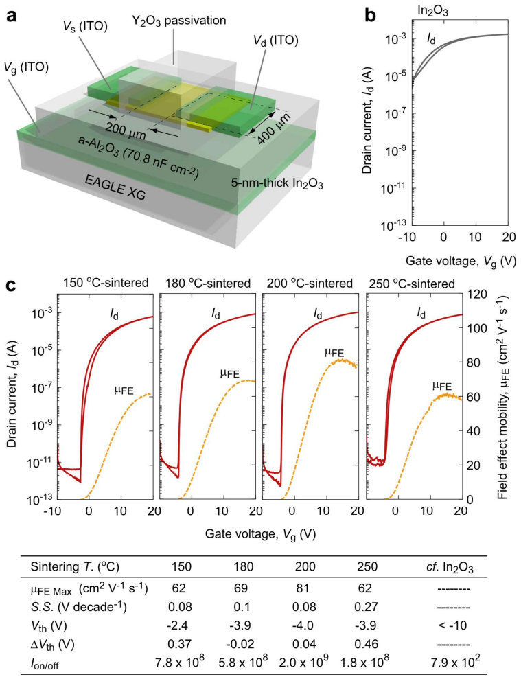
The central claim is that the hydrogen needed for high-mobility polycrystalline $\mathrm{In_2O_3}$ can be delivered from the deposition target itself. When an $\mathrm{In(OH)_3}$ ceramic target sintered at 150–250 °C is ablated by a KrF laser in oxygen, hydrogen is transferred into the growing film at concentrations near $10^{22}\ \mathrm{cm^{-3}}$, roughly thirty times higher than what residual chamber water supplies to a conventional $\mathrm{In_2O_3}$ target. That hydrogen keeps the as-grown film amorphous; after annealing at 300 °C in air, the film crystallizes with lateral grains up to ~2 µm, and the largest grains appear for the 200 °C-sintered target. TFTs fabricated from the 5-nm channel of this annealed film show a field-effect mobility of about $81\ \mathrm{cm^2\,V^{-1}s^{-1}}$ with small threshold-voltage shifts under bias stress, whereas TFTs from a conventional $\mathrm{In_2O_3}$ target do not turn off properly.
Load-bearing premise
The argument rests on the premise that the measured field-effect mobility of about $81\ \mathrm{cm^2\,V^{-1}s^{-1}}$ is caused by hydrogen-enabled large-grain crystallization in the 5-nm channel, not by contact resistance, channel-length correction, or an extraction artifact.
Editorial extensions
If this is right
- A target sintered at 200 °C produces the largest grains (~2 µm) and the highest field-effect mobility (~81 cm² V⁻¹ s⁻¹) among the four sintering temperatures tested.
- No external hydrogen source, gas cylinder, or chamber-pressure water-vapor method is needed; the same PLD system with the hydroxide target supplies hydrogen directly.
- The as-deposited films are amorphous and become large-grained after a 300 °C anneal, so the process is compatible with low-temperature backplane fabrication.
- The resulting TFTs show threshold-voltage shifts of 0.51 V under positive bias stress and 0.17 V under negative bias stress after 5000 s at room temperature.
- At ~81 cm² V⁻¹ s⁻¹, the mobility sits far above the ~5–10 cm² V⁻¹ s⁻¹ typical of amorphous IGZO, pointing toward backplanes for 8K and 240 Hz displays.
Reading between the lines
- Inference: the mobility claim would be tighter if Hall effect were measured on the same 5-nm channel thickness used in the transistor, since the reported Hall data are from 50-nm films.
- Inference: the four sintering temperatures vary hydrogen content and porosity together, so the grain-size-to-mobility correlation does not by itself isolate hydrogen as the cause; a test that varies hydrogen independently at one sintering temperature would separate the factors.
- Inference: the same hydroxide-target trick may generalize to other oxide semiconductors; hydroxide or hydrated-oxide targets of other cations such as Zn or In–Zn could deliver hydrogen to their respective channels by the same decomposition route.
- Inference: the lower carbon content measured in films from the hydroxide target hints at possible extra stability benefits, but the paper does not separate carbon effects from hydrogen effects.
Editorial analysis
A structured set of objections, weighed in public.
Referee Report
Summary. The manuscript proposes replacing gaseous or water-vapor hydrogen sources in pulsed laser deposition with a sintered In(OH)3 ceramic target, which releases hydrogen during ablation and incorporates it into as-deposited In2O3 films. The authors show that films grown from such targets are initially amorphous, retain hydrogen concentrations around 10^22 cm^-3, and after a 300 °C anneal develop large lateral grains (up to ~2 µm for a 200 °C-sintered target). They then fabricate bottom-gate In2O3 TFTs with Y2O3 passivation and report field-effect mobilities above 60 cm2 V^-1 s^-1, with a peak of ~81 cm2 V^-1 s^-1 for the 200 °C target, along with small threshold-voltage shifts under bias stress. The central claims are that the In(OH)3 target provides a safe, simple hydrogen incorporation route and that the incorporated hydrogen enables large-grain crystallization and high transistor mobility.
Significance. If the mobility and grain-growth claims are substantiated, the work offers a practically attractive manufacturing route to high-mobility In2O3-based TFTs without hydrogen gas handling, and this would be a useful contribution to oxide-display backplane research. The materials-level demonstration is credible: SIMS, XRD, EBSD, Hall, and transistor measurements are presented as independent evidence, and the hydrogen-incorporation step does not rely on fitted parameters. The main weakness is that the headline transistor mobility rests on a single extraction that is not reconciled with the Hall mobility of the same annealed films, and no device-to-device statistics or extraction controls are provided. The large-grain microstructure itself appears real, but the causal link to the reported 81 cm2 V^-1 s^-1 mobility is not yet established.
major comments (4)
- [Results and Discussion, Fig. 4c and Fig. S3 versus Fig. 7c] The central high-mobility claim is not reconciled with the Hall mobility data. Hall measurements on 50-nm annealed films give 10–20 cm2 V^-1 s^-1 (Fig. 4c and Fig. S3), whereas the 5-nm TFT channel yields μFE ≈ 81 cm2 V^-1 s^-1. The channel is thinner, deposited on a different substrate/stack, and processed with Y2O3 passivation plus a 350 °C anneal, so the comparison is not apples-to-apples; however, the manuscript offers no physical mechanism for why the thin-channel field-effect mobility should be four to eight times higher than the Hall mobility of the same material. Without such an explanation, or Hall data on thin films, the reported μFE value cannot be distinguished from an extraction artifact.
- [Experimental Section, Eq. (1) and device fabrication] The μFE extraction is insufficiently documented. The text states that W/L was 'corrected for patterning errors caused by film deposition through the stencil mask,' but the correction procedure is not described, no channel-length series is shown, no contact-resistance correction is reported, and no device-to-device statistics or error bars are given for any transistor parameter. Equation (1) is applied at Vd = 5 V, which may or may not be a valid linear-regime condition depending on Vth and the Vg range. Please provide the number of devices tested, the spread in μFE, representative transfer curves for all targets, and details of the W/L correction and the linearity check.
- [Results and Discussion, Fig. 6c and Fig. 7c] The causal link between large grains and high mobility is inferred from a four-point correlation across sintering temperatures, not from a controlled experiment that varies hydrogen independently. Sintering temperature simultaneously changes the target phase composition, density, porosity, and hydrogen content, so the correlation between grain size and μFE does not isolate the role of hydrogen. A test in which hydrogen concentration is varied while other deposition conditions are fixed (for example, by mixing In2O3 and In(OH)3 targets, or by changing the PLD background pressure) would substantially strengthen the mechanism claim.
- [Experimental Section, SIMS characterization and Fig. 4a–b] Absolute hydrogen concentrations of ~10^22 cm^-3 are quoted without calibration details. SIMS hydrogen quantification requires an implanted standard or a well-characterized reference, and matrix effects can be severe in oxide films. Because the comparison between the In(OH)3-derived films and the In2O3-target-derived films is load-bearing for the 'sufficient hydrogen' claim, the authors should state the calibration procedure, the estimated uncertainty, and how the surface/interface regions were excluded.
minor comments (5)
- [Throughout] There are numerous typographical errors, including 'demonstarate', 'centent', 'supprese', 'singnificant', 'decreas', 'appropiate', 'homogenious', 'temperatres', 'Phtograph', 'targtes', 'fablicated', and 'Gaussion'. A careful proofreading pass is needed.
- [References] Reference 27 (Ohta et al., Adv. Mater. 2004) concerns a transparent organic thin-film transistor with a laterally grown phthalocyanine channel and does not appear relevant to the Y2O3/Er2O3 passivation of In2O3 TFTs discussed in the introduction; please verify or replace this citation.
- [Figure S2 caption] The caption attributes the increased SIMS carbon signal in the 150 °C-sintered-target film to a matrix effect at the underlying SiO2 interface, but the text in the main manuscript does not discuss this artifact; please clarify in the main text how the carbon comparison was made.
- [Figure S3 and Fig. 4c] The Hall mobility and carrier concentration are reported without error bars or measurement uncertainty, which makes it difficult to judge whether differences between targets and between as-deposited and annealed states are significant.
- [Introduction and Conclusions] The phrase 'breakthrough' in the title and 'very high electron mobility' in the abstract overstate the current evidence given the unresolved Hall/FET discrepancy; a more measured wording would be more appropriate for the present data set.
Circularity Check
No significant circularity: the hydrogen-incorporation, grain-growth, and transistor claims are supported by independent measurements within the paper.
full rationale
The paper's central claim is that sintered In(OH)3 ceramic targets deliver hydrogen into PLD-grown In2O3 films without external hydrogen gas, and that this hydrogen suppresses premature crystallization and enables large-grain growth after annealing. Each link in that chain is supported by direct, in-paper measurements rather than by definition or by fitting. SIMS depth profiles show ~1e22 cm-3 hydrogen in films from the In(OH)3 target versus ~3e20 cm-3 from a conventional In2O3 target (Fig. 4a-b). XRD and EBSD show that as-deposited In(OH)3-target films are amorphous while In2O3-target films are already polycrystalline, and that only the hydrogen-rich films develop micrometer-scale grains upon annealing (Figs. 5-6). These are controlled comparisons, not quantities defined in terms of the target result. The field-effect mobility is extracted with the standard transconductance formula, Eq. (1), from measured transfer curves; no parameter is fitted to the reported 81 cm2 V-1 s-1 value and no prediction is claimed from a fitted input. Citations to prior work by Magari and co-workers (refs 25-30) provide background and mechanistic context, but the paper's own control experiments independently establish the hydrogen-grain-growth correlation, so those citations are not load-bearing in a circular sense. The unresolved discrepancy between Hall mobility (10-20 cm2 V-1 s-1 on 50-nm films) and TFT field-effect mobility (~81 cm2 V-1 s-1 on 5-nm channels), and the undocumented W/L patterning correction, are legitimate scientific and reporting concerns about the strength of the mobility claim, but they are not circularity: the mobility value is not assumed in order to derive itself. No self-definitional, fitted-input-as-prediction, or author-imported-uniqueness pattern is present. The derivation chain is self-contained against its own measurements, so the circularity score is 0.
Assumptions & free parameters
assumptions (4)
- domain assumption Hydrogen atoms from the In(OH)3 target survive the PLD plasma and incorporate into the growing film, suppressing crystallization during deposition.
- domain assumption SIMS hydrogen counts are linearly proportional to concentration and can be compared across samples without explicit calibration standards.
- domain assumption Annealing at 300 degrees Celsius removes oxygen vacancies, which lowers carrier concentration, while residual hydrogen remains and does not directly affect mobility.
- domain assumption The largest lateral grain size observed by EBSD is the cause of the highest TFT field-effect mobility.
Cite this review
Pith. "Pith review of Indium Hydroxide Ceramic Targets: A Breakthrough in High-Mobility Thin-Film Transistor Technology." pith.science (2026). https://pith.science/paper/7JVERW7Q
@misc{pith2026250711011,
  author       = {Pith},
  title        = {Pith review of: Indium Hydroxide Ceramic Targets: A Breakthrough in High-Mobility Thin-Film Transistor Technology},
  year         = {2026},
  howpublished = {\url{https://pith.science/paper/7JVERW7Q}},
  note         = {Machine review of arXiv:2507.11011}
}
read the original abstract
Thin-film transistors composed of a hydrogen-containing indium oxide active layer are promising candidates for backplane devices in next-generation flat panel displays, offering higher definition and faster operation. However, the hydrogen incorporation process during film deposition poses challenges for scalable and industrial development due to both safety and controllability issues. Here, we demonstrate that using indium hydroxide ceramic as the target material for film deposition overcomes the difficulties associated with hydrogen gas usage. We sintered commercially available indium hydroxide powder using a conventional ceramic process at 150-250{\deg}C in air and utilized it for the deposition of hydrogen-incorporated indium oxide films via pulsed laser deposition. The resulting indium oxide films, after thermal annealing, contained a sufficient concentration of hydrogen and exhibited very high electron mobility due to significantly grown grains. Furthermore, we confirmed that the fabricated thin-film transistors exhibited comparably high performance to those produced using the gas-phase hydrogen incorporation method. This approach offers a practical pathway for hydrogen-containing indium oxide-based thin-film transistors in next-generation flat panel displays.
Figures


Figures from the paper (4 more)


Reference graph
Works this paper leans on
-
[1]
Novel top‐gate zinc oxide thin‐film transistors (ZnO TFTs) for AMLCDs
(1) Hirao, T.; Furuta, M.; Furuta, H.; Matsuda, T.; Hiramatsu, T.; Hokari, H.; Yoshida, M.; Ishii, H.; Kakegawa, M. Novel top‐gate zinc oxide thin‐film transistors (ZnO TFTs) for AMLCDs. Journal of the Society for Information Display 2007, 15 (1), 17-22. DOI: 10.1889/1.2451545. (2) Kamiya, T.; Hosono, H. Material characteristics and applications of transp...
-
[1078]
DOI: 10.1038/s41467- 022-28480-9. (26) Ghediya, P. R.; Magari, Y .; Sadahira, H.; Endo, T.; Furuta, M.; Zhang, Y .; Matsuo, Y .; Ohta, H. Reliable Operation in High-Mobility Indium Oxide Thin Film Transistors. Small Methods 2025, 9 (1), e2400578. DOI: 10.1002/smtd.202400578 From NLM PubMed-not-MEDLINE. (27) Ohta, H.; Kambayashi, T.; Nomura, K.; Hirano, M....
Reviewed August 6, 2026 · model on record in the stance chip above.
Discussion (0). Continue with ORCID to comment.