First-principles calculations of electrical conductivities of edge-modified graphene nanoribbons: strain effect
Pith reviewed 2026-05-19 20:27 UTC · model grok-4.3
The pith
Strain turns nonconductive armchair graphene nanoribbons into conductors across infrared to ultraviolet energies.
A machine-rendered reading of the paper's core claim, the machinery that carries it, and where it could break.
Core claim
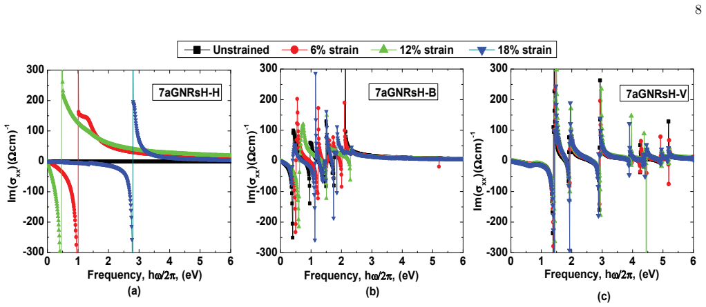
Pristine unstrained 7aGNRsH is electrically nonconductive but turns electrically conductive in a wide energy spectrum from IR to visible to UV due to strain engineering, while metallic unstrained and strained 7aGNRsH-B and 7aGNRsH-V show non-vanishing conductivity in those regimes; strain localizes fermions near the Gamma-point for the semiconducting case and keeps them away for the metallic cases.
What carries the argument
First-principles DFT calculations of electrical conductivity and Berry curvature as functions of applied strain on edge-modified 7aGNRsH, 7aGNRsH-B, and 7aGNRsH-V nanoribbons.
If this is right
- Strain engineering provides a route to activate conductivity in semiconducting nanoribbons for broad-spectrum optoelectronic devices.
- Berry curvature localization near the Gamma point under strain alters fermion spread and may change transport behavior.
- Two-boron-atom doped versions produce large infrared conductivity peaks that could be observed in synthesized samples.
- Edge modifications such as boron doping or vacancies keep the nanoribbons metallic with non-vanishing conductivity independent of strain.
Where Pith is reading between the lines
- The predicted infrared conductivity peaks in two-boron-doped ribbons could guide targeted experiments on the referenced JACS structures.
- Out-of-plane deformations induced by strain may link these electronic changes to mechanical flexibility in future nanoribbon devices.
- Similar strain responses might appear in other widths or edge chemistries, suggesting a general pattern for tuning 2D carbon systems.
- Device architectures could exploit the metallic persistence in doped ribbons for stable sensor operation under varying strain.
Load-bearing premise
The chosen supercell models and standard density functional theory accurately describe real electronic transport and Berry curvature under strain without large errors from exchange-correlation functional, k-point sampling, or missing many-body effects.
What would settle it
Direct measurement of electrical conductivity on experimentally strained pristine 7aGNRsH samples that shows no conductivity gain across the infrared-to-ultraviolet range.
Figures




read the original abstract
We investigate the influence of strain on the electrical properties of graphene nanoribbons that have potential applications in making sensors and other optoelectronic devices. In particular, we chose pristine armchair graphene nanoribbons with 7 zigzag edges (7aGNRsH), boron doped armchair graphene nanoribbons with 7 zigzag edges (7aGNRsH-B) and armchair graphene nanoribbons with 7 zigzag edges that have one carbon atom vacancy (7aGNRsH-V). Based on first-principles calculations, results show that pristine unstrained 7aGNRsH is electrically nonconductive but turns to be electrically conductive in a wide range of energy spectrum, e.g., from IR to visible to UV, due to the application of strain engineering. In metallic unstrained and strained 7aGNRsH-B and 7aGNRsH-V, non-vanishing electrical conductivity in the IR, visible and UV energy spectrum regimes are observed. We also investigate the influence of strain on the Berry curvature of 7aGNRsH, 7aGNRsH-B and 7aGNRsH-V nanoribbons. The results show that fermions are spread through out the Brillion zone in the reciprocal space for semiconducting unstrained 7aGNRsH but localized near the $\Gamma$-point for strained 7aGNRsH that have out-of-plane deformations due to strain engineering. For metallics 7aGNRsH-B and 7aGNRsH-V, Berry curvature plots show that fermions are localized far away from the $\Gamma$-point. In two atom boron doped p-type armchair graphene nanoribbons with 7 zigzag edges (7aGNRsH-2B), large peaks in electrical conductivity at IR energy spectrum regimes can be observed. These peaks of electrical conductivities in 7aGNRSH-2B may be detectable in experimentally synthesized structure in Reference, JACS 137, 8872 (2016).
Editorial analysis
A structured set of objections, weighed in public.
Referee Report
Summary. The manuscript uses first-principles calculations to examine strain effects on electrical conductivity and Berry curvature in pristine 7aGNRsH armchair graphene nanoribbons and their edge-modified variants (boron-doped 7aGNRsH-B, vacancy 7aGNRsH-V, and two-atom boron 7aGNRsH-2B). The central claims are that unstrained pristine 7aGNRsH is nonconductive but strain engineering induces finite conductivity across IR to visible to UV ranges; metallic unstrained/strained doped and defective variants exhibit non-vanishing conductivity in those regimes; and strain-induced out-of-plane deformations localize Berry curvature near the Γ point while metallic cases show localization away from Γ. A secondary claim notes large IR conductivity peaks in 7aGNRsH-2B potentially detectable in experiment.
Significance. If the computational results hold after proper validation, the work would indicate strain as a viable route to engineer optoelectronic response in GNRs for sensor and device applications, with the reported conductivity peaks in the 2B-doped case offering a concrete experimental target. The Berry curvature analysis adds insight into strain-tuned topological features. However, the absence of methodological specifics and benchmarks against known limits reduces the immediate impact and reproducibility of the quantitative predictions.
major comments (2)
- [Abstract] Abstract and implied Methods: the headline result that strain closes or sufficiently reduces the gap in pristine 7aGNRsH to produce conductivity from IR through UV depends on an accurate description of the bandgap and its strain dependence. Standard semilocal DFT functionals systematically underestimate gaps in armchair GNRs; no information is supplied on the exchange-correlation functional, k-point sampling, supercell convergence, or any scissor/GW/hybrid correction. This directly affects both the critical strain value and the absolute energy ranges reported for conductivity onset.
- [Abstract] Abstract: the claim of non-vanishing conductivity in metallic 7aGNRsH-B and 7aGNRsH-V across IR–visible–UV, and the localization of Berry curvature near Γ only for out-of-plane strained 7aGNRsH, cannot be assessed without details on how strain is applied (uniaxial vs. biaxial, in-plane vs. out-of-plane components) or how conductivity is computed (e.g., Kubo formula, Boltzmann transport, or direct band-structure integration).
minor comments (2)
- [Abstract] Abstract: 'Brillion zone' should read 'Brillouin zone'; 'through out' should read 'throughout'; capitalization of '7aGNRSH-2B' is inconsistent with earlier '7aGNRsH-2B'.
- [Abstract] Abstract: the reference 'JACS 137, 8872 (2016)' should be given a full bibliographic entry and properly cited in the text.
Simulated Author's Rebuttal
We thank the referee for the careful review and constructive comments on our manuscript. We address each major comment below and will revise the manuscript to improve methodological transparency and reproducibility.
read point-by-point responses
-
Referee: [Abstract] Abstract and implied Methods: the headline result that strain closes or sufficiently reduces the gap in pristine 7aGNRsH to produce conductivity from IR through UV depends on an accurate description of the bandgap and its strain dependence. Standard semilocal DFT functionals systematically underestimate gaps in armchair GNRs; no information is supplied on the exchange-correlation functional, k-point sampling, supercell convergence, or any scissor/GW/hybrid correction. This directly affects both the critical strain value and the absolute energy ranges reported for conductivity onset.
Authors: We agree that the absence of explicit methodological details limits assessment of the quantitative results. In the revised manuscript we will add a dedicated Methods section specifying the PBE exchange-correlation functional, Monkhorst-Pack k-point sampling, supercell sizes used for convergence testing, and confirmation that no scissor, GW or hybrid corrections were applied. We will also add a brief discussion of the known bandgap underestimation in semilocal DFT and its implications for the reported conductivity onsets, while noting that the qualitative strain-induced changes remain the central finding. revision: yes
-
Referee: [Abstract] Abstract: the claim of non-vanishing conductivity in metallic 7aGNRsH-B and 7aGNRsH-V across IR–visible–UV, and the localization of Berry curvature near Γ only for out-of-plane strained 7aGNRsH, cannot be assessed without details on how strain is applied (uniaxial vs. biaxial, in-plane vs. out-of-plane components) or how conductivity is computed (e.g., Kubo formula, Boltzmann transport, or direct band-structure integration).
Authors: We will expand the manuscript to provide the requested details. Strain is applied uniaxially along the periodic direction of the nanoribbon with full atomic relaxation, which naturally produces out-of-plane buckling components. Electrical conductivity is evaluated from the Kubo-Greenwood formula within linear-response theory using the DFT band structure and velocity matrix elements. Berry curvature is obtained from the Berry connection of the Bloch states. These specifications, together with any relevant convergence parameters, will be added to the revised text. revision: yes
Circularity Check
No circularity: direct first-principles outputs with no fitted predictions or self-referential reductions
full rationale
The manuscript performs standard DFT computations of band structures, conductivities, and Berry curvatures for strained and edge-modified armchair GNRs. All reported quantities (e.g., strain-induced metallization in 7aGNRsH, conductivity spectra, and localization of Berry curvature near Γ) are direct numerical outputs of the chosen functional, supercell, and k-point sampling rather than quantities obtained by fitting a parameter to one subset of the same data and then relabeling the result as a prediction. No equations or claims reduce the conductivity or curvature results to self-defined inputs, and the single external citation (JACS 2016) is used only for experimental context, not as a load-bearing uniqueness theorem or ansatz. The derivation chain is therefore self-contained and independent of the paper's own fitted values.
Axiom & Free-Parameter Ledger
free parameters (1)
- applied strain magnitude
axioms (1)
- domain assumption Standard density-functional theory approximations (Born-Oppenheimer, chosen exchange-correlation functional) suffice to describe electronic structure and transport in these nanoribbons.
Lean theorems connected to this paper
-
IndisputableMonolith/Foundation/RealityFromDistinction.leanreality_from_one_distinction unclear?
unclearRelation between the paper passage and the cited Recognition theorem.
Based on first-principles calculations... we use the Quantum Espresso software package and the wannier90 program... Ultrasoft pseudopotentials and a plane wave basis set with kinetic energy and charge density cut-off at 100 Ry and 800 Ry... Perdew-Burke-Ernzerhof (PBE) Functional
-
IndisputableMonolith/Cost/FunctionalEquation.leanwashburn_uniqueness_aczel unclear?
unclearRelation between the paper passage and the cited Recognition theorem.
For calculation of Berry curvature, quantum and electrical conductivities, we have used maximally localized Wannier functions method... Kubo-Greenwood formalism
What do these tags mean?
- matches
- The paper's claim is directly supported by a theorem in the formal canon.
- supports
- The theorem supports part of the paper's argument, but the paper may add assumptions or extra steps.
- extends
- The paper goes beyond the formal theorem; the theorem is a base layer rather than the whole result.
- uses
- The paper appears to rely on the theorem as machinery.
- contradicts
- The paper's claim conflicts with a theorem or certificate in the canon.
- unclear
- Pith found a possible connection, but the passage is too broad, indirect, or ambiguous to say the theorem truly supports the claim.
Reference graph
Works this paper leans on
-
[1]
X. Liu, Z. Hao, E. Khalaf, J. Y. Lee, Y. Ronen, H. Yoo, D. H. Najafabadi, K. Watanabe, T. Taniguchi, A. Vish- wanath, et al., Tunable spin-polarized correlated states in twisted double bilayer graphene, Nature 583, 221 (2020)
work page 2020
-
[2]
L. Balents, C. R. Dean, D. K. Efetov, and A. F. Young, Superconductivity and strong correlations in moir´ e flat bands, Nature Physics 16, 725 (2020)
work page 2020
-
[3]
X. Liu, Z. Wang, K. Watanabe, T. Taniguchi, O. Vafek, and J. Li, Tuning electron correlation in magic-angle twisted bilayer graphene using coulomb screening, Sci- ence 371, 1261 (2021)
work page 2021
-
[4]
D. E. Parker, T. Soejima, J. Hauschild, M. P. Zaletel, N. Bultinck, et al. , Strain-induced quantum phase tran- sitions in magic-angle graphene, Physical review letters 127, 027601 (2021)
work page 2021
-
[5]
A. K. Geim and K. S. Novoselov, The rise of graphene, Nat. Mater. 6, 183 (2007)
work page 2007
-
[6]
J. N. Coleman, M. Lotya, A. O’Neill, S. D. Bergin, P. J. King, U. Khan, K. Young, A. Gaucher, S. De, R. J. Smith, I. V. Shvets, S. K. Arora, G. Stanton, H.-Y. Kim, K. Lee, G. T. Kim, G. S. Duesberg, T. Hallam, J. J. Boland, J. J. Wang, J. F. Donegan, J. C. Grunlan, G. Mo- riarty, A. Shmeliov, R. J. Nicholls, J. M. Perkins, E. M. Grieveson, K. Theuwissen, ...
work page 2011
-
[7]
K. S. Novoselov, A. K. Geim, S. V. Morozov, D. Jiang, M. I. Katsnelson, I. V. Grigorieva, S. V. Dubonos, and A. A. Firsov, Two-dimensional gas of massless dirac fermions in graphene, Nature 438, 197 (2005)
work page 2005
-
[8]
K. S. Novoselov, D. Jiang, F. Schedin, T. J. Booth, V. V. Khotkevich, S. V. Morozov, and A. K. Geim, Two- dimensional atomic crystals, Proc. Natl. Acad. Sci. USA 102, 10451 (2005)
work page 2005
-
[9]
K. S. Novoselov, A. K. Geim, S. V. Morozov, D. Jiang, Y. Zhang, S. V. Dubonos, I. V. Grigorieva, and A. A. Firsov, Electric field effect in atomically thin carbon films, Science 306, 666 (2004)
work page 2004
-
[10]
Savage, Materials science: Super carbon, Nature 483, S30 (2012)
N. Savage, Materials science: Super carbon, Nature 483, S30 (2012). 12
work page 2012
-
[11]
L. Liao, Y.-C. Lin, M. Bao, R. Cheng, J. Bai, Y. Liu, Y. Qu, K. L. Wang, Y. Huang, and X. Duan, High-speed graphene transistors with a self-aligned nanowire gate, Nature 467, 305 (2010)
work page 2010
-
[12]
H. Aoki and M. S. Dresselhaus, Physics of graphene (Springer Science & Business Media, 2013)
work page 2013
-
[13]
B. Trauzettel, D. V. Bulaev, D. Loss, and G. Burkard, Spin qubits in graphene quantum dots, Nature Physics 3, 192 (2007)
work page 2007
-
[14]
M. Y. Han, B. ¨Ozyilmaz, Y. Zhang, and P. Kim, Energy band-gap engineering of graphene nanoribbons, Phys. Rev. Lett. 98, 206805 (2007)
work page 2007
-
[15]
S. Y. Zhou, G.-H. Gweon, A. Fedorov, d. First, PN, W. De Heer, D.-H. Lee, F. Guinea, A. C. Neto, and A. Lanzara, Substrate-induced bandgap opening in epi- taxial graphene, Nat. Mater. 6, 770 (2007)
work page 2007
-
[16]
F. Xia, D. B. Farmer, Y.-m. Lin, and P. Avouris, Graphene field-effect transistors with high on/off current ratio and large transport band gap at room temperature, Nano Lett. 10, 715 (2010)
work page 2010
-
[17]
Y.-C. Chen, T. Cao, C. Chen, Z. Pedramrazi, D. Haberer, D. G. De Oteyza, F. R. Fischer, S. G. Louie, and M. F. Crommie, Molecular bandgap engineering of bottom-up synthesized graphene nanoribbon heterojunctions, Nat. Nanotechnol. 10, 156 (2015)
work page 2015
-
[18]
M. M. Ugeda, A. J. Bradley, S.-F. Shi, H. Felipe, Y. Zhang, D. Y. Qiu, W. Ruan, S.-K. Mo, Z. Hussain, Z.-X. Shen, et al. , Giant bandgap renormalization and excitonic effects in a monolayer transition metal dichalco- genide semiconductor, Nat. Mater. 13, 1091 (2014)
work page 2014
-
[19]
L. Brey and H. A. Fertig, Electronic states of graphene nanoribbons studied with the dirac equation, Phys. Rev. B 73, 235411 (2006)
work page 2006
-
[20]
E. Mishchenko, Minimal conductivity in graphene: In- teraction corrections and ultraviolet anomaly, EPL (Eu- rophysics Letters) 83, 17005 (2008)
work page 2008
-
[21]
A. R. Wright, J. C. Cao, and C. Zhang, Enhanced opti- cal conductivity of bilayer graphene nanoribbons in the terahertz regime, Phys. Rev. Lett. 103, 207401 (2009)
work page 2009
- [22]
-
[23]
T. Stauber, N. M. R. Peres, and A. K. Geim, Optical conductivity of graphene in the visible region of the spec- trum, Phys. Rev. B 78, 085432 (2008)
work page 2008
- [24]
- [25]
-
[26]
F. Hipolito, D. Dimitrovski, and T. G. Pedersen, Iter- ative approach to arbitrary nonlinear optical response functions of graphene, Phys. Rev. B 99, 195407 (2019)
work page 2019
-
[27]
S. A. Herrera and G. G. Naumis, Electronic and optical conductivity of kekul´ e-patterned graphene: Intravalley and intervalley transport, Physical Review B 101, 205413 (2020)
work page 2020
-
[28]
D. Van Tuan, J. Marmolejo-Tejada, X. Waintal, B. Nikoli´ c, S. O. Valenzuela, and S. Roche, Spin hall effect and origins of nonlocal resistance in adatom- decorated graphene, Physical review letters 117, 176602 (2016)
work page 2016
-
[29]
G. De Filippis, V. Cataudella, A. de Candia, A. S. Mishchenko, and N. Nagaosa, Alternative representation of the kubo formula for the optical conductivity: A short- cut to transport properties, Phys. Rev. B 90, 014310 (2014)
work page 2014
-
[30]
P. Gallagher, C.-S. Yang, T. Lyu, F. Tian, R. Kou, H. Zhang, K. Watanabe, T. Taniguchi, and F. Wang, Quantum-critical conductivity of the dirac fluid in graphene, Science 364, 158 (2019)
work page 2019
-
[31]
B. N. Narozhny, Optical conductivity in graphene: Hy- drodynamic regime, Phys. Rev. B 100, 115434 (2019)
work page 2019
- [32]
- [33]
-
[34]
V. Gusynin, S. Sharapov, and J. Carbotte, Unusual mi- crowave response of dirac quasiparticles in graphene, Physical review letters 96, 256802 (2006)
work page 2006
-
[35]
M. Mojarro, R. Carrillo-Bastos, and J. A. Maytorena, Optical properties of massive anisotropic tilted dirac sys - tems, Physical Review B 103, 165415 (2021)
work page 2021
-
[36]
H. Falomir, M. Loewe, E. Mu˜ noz, and A. Raya, Optical conductivity and transparency in an effective model for graphene, Physical Review B 98, 195430 (2018)
work page 2018
- [37]
-
[38]
R. R. Cloke, T. Marangoni, G. D. Nguyen, T. Joshi, D. J. Rizzo, C. Bronner, T. Cao, S. G. Louie, M. F. Crommie, and F. R. Fischer, Site-specific substitutional boron dop- ing of semiconducting armchair graphene nanoribbons, Journal of the American Chemical Society 137, 8872 (2015)
work page 2015
-
[39]
S. Prabhakar, R. Nepal, R. Melnik, and A. A. Kovalev, Valley-dependent lorentz force and aharonov-bohm phase in strained graphene p− n junction, Phys. Rev. B 99, 094111 (2019)
work page 2019
-
[40]
Deepika, T. J. D. Kumar, A. Shukla, and R. Kumar, Edge configurational effect on band gaps in graphene nanorib- bons, Phys. Rev. B 91, 115428 (2015)
work page 2015
-
[41]
H. Lim, J. Jung, R. S. Ruoff, and Y. Kim, Structurally driven one-dimensional electron confinement in sub-5-nm graphene nanowrinkles, Nat. Commun. 6, 8601 (2015)
work page 2015
-
[42]
W. Bao, F. Miao, Z. Chen, H. Zhang, W. Jang, C. Dames, and C. N. Lau, Controlled ripple texturing of suspended graphene and ultrathin graphite membranes, Nat. Nan- otechnol. 4, 562 (2009)
work page 2009
-
[43]
S. Prabhakar, R. Melnik, and L. Bonilla, Pseudospin life- time in relaxed-shape armchair graphene nanoribbons due to in-plane phonon modes, Phys. Rev. B 93, 115417 (2016)
work page 2016
-
[44]
R. B. Christensen, T. Frederiksen, and M. Brandbyge, Identification of pristine and defective graphene nanorib- bons by phonon signatures in the electron transport char- acteristics, Phys. Rev. B 91, 075434 (2015)
work page 2015
-
[45]
S. Prabhakar, R. Melnik, and A. Inomata, Geometric spin manipulation in semiconductor quantum dots, Applied Physics Letters 104, 142411 (2014). 13
work page 2014
-
[46]
C. Lee, X. Wei, J. W. Kysar, and J. Hone, Measurement of the elastic properties and intrinsic strength of mono- layer graphene, Science 321, 385 (2008)
work page 2008
-
[47]
E. Khestanova, F. Guinea, L. Fumagalli, A. Geim, and I. Grigorieva, Universal shape and pressure inside bub- bles appearing in van der waals heterostructures, Nat. Commun. 7, 12587 (2016)
work page 2016
-
[48]
F. Ding, H. Ji, Y. Chen, A. Herklotz, K. D¨ orr, Y. Mei, A. Rastelli, and O. G. Schmidt, Stretchable graphene: a close look at fundamental parameters through biaxial straining, Nano Lett. 10, 3453 (2010)
work page 2010
-
[49]
Z. H. Ni, W. Chen, X. F. Fan, J. L. Kuo, T. Yu, A. T. S. Wee, and Z. X. Shen, Raman spectroscopy of epitaxial graphene on a sic substrate, Phys. Rev. B 77, 115416 (2008)
work page 2008
-
[50]
R. Carrillo-Bastos, C. Le´ on, D. Faria, A. Latg´ e, E. Y. Andrei, and N. Sandler, Strained fold-assisted transport in graphene systems, Phys. Rev. B 94, 125422 (2016)
work page 2016
-
[51]
M. S. Bronsgeest, N. Bendiab, S. Mathur, A. Kimouche, H. T. Johnson, J. Coraux, and P. Pochet, Strain relax- ation in cvd graphene: Wrinkling with shear lag, Nano Lett. 15, 5098 (2015)
work page 2015
-
[52]
E. Cerda and L. Mahadevan, Geometry and physics of wrinkling, Phys. Rev. Lett. 90, 074302 (2003)
work page 2003
-
[53]
R. J. T. Nicholl, N. V. Lavrik, I. Vlassiouk, B. R. Sri- janto, and K. I. Bolotin, Hidden area and mechanical nonlinearities in freestanding graphene, Phys. Rev. Lett. 118, 266101 (2017)
work page 2017
-
[54]
N. Ferralis, R. Maboudian, and C. Carraro, Evidence of structural strain in epitaxial graphene layers on 6h-sic (0001), Phys. Rev. Lett. 101, 156801 (2008)
work page 2008
-
[55]
D. Boyd, W.-H. Lin, C.-C. Hsu, M. Teague, C.-C. Chen, Y.-Y. Lo, W.-Y. Chan, W.-B. Su, T.-C. Cheng, C.-S. Chang, et al. , Single-step deposition of high-mobility graphene at reduced temperatures, Nat. Commun. 6, 6620 (2015)
work page 2015
-
[56]
Z. Peng, X. Chen, Y. Fan, D. J. Srolovitz, and D. Lei, Strain engineering of 2d semiconductors and graphene: from strain fields to band-structure tuning and photonic applications, Light: Science & Applications 9, 1 (2020)
work page 2020
-
[57]
A. A. Griffith, Vi. the phenomena of rupture and flow in solids, Philosophical Transactions of the Royal Society of London 221, 163 (1921)
work page 1921
- [58]
-
[59]
I. I. Naumov and A. M. Bratkovsky, Gap opening in graphene by simple periodic inhomogeneous strain, Phys. Rev. B 84, 245444 (2011)
work page 2011
-
[60]
P. Giannozzi, S. Baroni, N. Bonini, M. Calandra, R. Car, C. Cavazzoni, D. Ceresoli, G. L. Chiarotti, M. Cococ- cioni, I. Dabo, et al. , Quantum espresso: a modular and open-source software project for quantum simula- tions of materials, Journal of physics: Condensed matter 21, 395502 (2009)
work page 2009
- [61]
-
[62]
J. P. Perdew, K. Burke, and M. Ernzerhof, Generalized gradient approximation made simple, Physical review let- ters 77, 3865 (1996)
work page 1996
-
[63]
A. Kokalj, Xcrysden - a new program for displaying crystalline structures and electron densities, Journal of Molecular Graphics and Modelling 17, 176 (1999)
work page 1999
-
[64]
M. Topsakal, E. Akt¨ urk, H. Sevin¸ cli, and S. Ciraci, First- principles approach to monitoring the band gap and mag- netic state of a graphene nanoribbon via its vacancies, Phys. Rev. B 78, 235435 (2008)
work page 2008
-
[65]
Zak, Berry phase for energy bands in solids, Physical review letters 62, 2747 (1989)
J. Zak, Berry phase for energy bands in solids, Physical review letters 62, 2747 (1989)
work page 1989
-
[66]
Blount, Formalisms of band theory, Solid state physics , 13, 305 (1962)
E. Blount, Formalisms of band theory, Solid state physics , 13, 305 (1962)
work page 1962
- [67]
discussion (0)
Sign in with ORCID, Apple, or X to comment. Anyone can read and Pith papers without signing in.