Cathodoluminescence Analysis of Defects and Grain Boundaries in Zn3P2 Thin Films Grown on Graphene by MOVPE and MBE
Pith reviewed 2026-05-25 04:08 UTC · model grok-4.3
The pith
Grain boundaries in Zn3P2 films quench excited carriers over several micrometers, reducing device suitability, while MOVPE growth on graphene produces larger grains than MBE.
A machine-rendered reading of the paper's core claim, the machinery that carries it, and where it could break.
Core claim
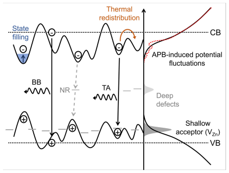
Quasi-van der Waals epitaxy of Zn3P2 on graphene by MOVPE produces films in which the density of antiphase boundaries correlates with optical emission modulation, while grain boundaries act as non-radiative sinks for excited charge carriers with the quenching effect extending several micrometers into the grains; MOVPE films also exhibit larger grains and suppressed strain-related sub-bandgap emission relative to MBE-grown films, directly linking extended defects to recombination pathways.
What carries the argument
Correlative electron microscopy and cathodoluminescence mapping that spatially links antiphase boundaries and grain boundaries to local emission intensity.
If this is right
- Grain-size control becomes a necessary step to reduce non-radiative losses in Zn3P2 absorbers.
- Antiphase-boundary density can be used as a proxy for emission uniformity in quasi-van der Waals grown films.
- MOVPE on graphene offers a route to lower strain-related sub-bandgap states compared with MBE.
- Device modeling must incorporate recombination lengths of several micrometers when grain boundaries are present.
Where Pith is reading between the lines
- If the quenching distance is material-intrinsic, then grain diameters must exceed roughly ten micrometers to keep most of the volume away from boundary losses.
- The observed suppression of sub-bandgap emission in MOVPE films suggests that thermal-expansion mismatch is mitigated more effectively by the van der Waals interface than by direct epitaxy.
- Similar extended recombination zones may appear in other earth-abundant absorbers that crystallize with high defect densities on mismatched substrates.
Load-bearing premise
That the cathodoluminescence contrast at boundaries and the extended quenching regions reflect intrinsic material properties rather than growth-specific or excitation-induced artifacts.
What would settle it
A measurement showing that the spatial extent of carrier quenching at grain boundaries shrinks below one micrometer when the same film is examined with a lower electron-beam energy or after surface passivation.
Figures


read the original abstract
Zn3P2 is a promising earth-abundant absorber for thin-film photovoltaics, yet its development is hindered by the lack of lattice-matched substrates, its incompatible thermal expansion coefficient, and a complex defect landscape. Here, we demonstrate the quasi-van der Waals epitaxy of Zn3P2 on graphene by metal-organic vapour phase epitaxy (MOVPE) and directly link the density of antiphase boundaries to optical emission modulation using correlative electron microscopy and cathodoluminescence (CL). Moreover, it is observed through CL that grain boundaries act as non-radiative sinks for excited charge carriers. The effect extends several micrometres into the grains, making grain boundaries detrimental to the applicability of Zn3P2 in read devices. Further comparison with molecular beam epitaxy grown films reveals the suppression of strain-related sub-bandgap emission in MOVPE-grown material. Overall, quasi-van der Waals epitaxy of Zn3P2 by MOVPE resulted in larger grains and improved material quality. In addition, these results directly link extended defects to recombination pathways in Zn3P2 and highlight grain-size control as a key strategy for improving earth-abundant photovoltaic absorbers.
Editorial analysis
A structured set of objections, weighed in public.
Referee Report
Summary. The manuscript reports quasi-van der Waals epitaxy of Zn3P2 thin films on graphene by MOVPE and MBE. Using correlative electron microscopy and cathodoluminescence, it links antiphase boundary density to optical emission modulation and shows that grain boundaries act as non-radiative sinks for excited carriers, with quenching extending several micrometres into grains. MOVPE films exhibit larger grains and suppressed strain-related sub-bandgap emission relative to MBE, leading to the conclusion that grain-size control is key for improving Zn3P2 photovoltaic performance.
Significance. If the CL observations are shown to reflect intrinsic bulk recombination rather than measurement artifacts, the work would strengthen understanding of extended defects in Zn3P2 and support grain-size engineering as a practical route to better earth-abundant absorbers. The correlative microscopy approach and direct MOVPE-MBE comparison are positive features that could inform growth optimization in related materials.
major comments (2)
- [CL results on grain boundaries] In the cathodoluminescence results and discussion sections, the claim that grain boundaries produce non-radiative quenching zones several micrometres wide (and are therefore detrimental to device applicability) rests on qualitative image contrast without reported line profiles, intensity decay lengths, or statistical sampling across multiple boundaries. This quantitative gap is load-bearing for the central performance-limiter conclusion.
- [Growth-method comparison] The MOVPE versus MBE comparison attributes suppression of sub-bandgap emission to larger grains and reduced strain, yet does not address or control for possible differences in surface termination, excitation conditions, or residual growth-induced defects that could produce the same spectral change. This assumption is load-bearing for the claim of improved material quality.
minor comments (2)
- [Abstract] Abstract: 'read devices' is presumably a typographical error for 'real devices'.
- [Methods] The manuscript would benefit from explicit statements on the electron-beam energy, current, and dwell time used for CL maps, as these parameters directly affect the probed volume and possible beam-induced artifacts.
Simulated Author's Rebuttal
We thank the referee for their constructive and detailed comments, which help clarify the presentation of our results. We address each major comment below and indicate the revisions that will be incorporated.
read point-by-point responses
-
Referee: [CL results on grain boundaries] In the cathodoluminescence results and discussion sections, the claim that grain boundaries produce non-radiative quenching zones several micrometres wide (and are therefore detrimental to device applicability) rests on qualitative image contrast without reported line profiles, intensity decay lengths, or statistical sampling across multiple boundaries. This quantitative gap is load-bearing for the central performance-limiter conclusion.
Authors: We agree that the original presentation relied on qualitative CL image contrast. In the revised manuscript we will extract and display line profiles across multiple grain boundaries from the existing CL maps, report the measured intensity decay lengths, and include statistical sampling over several boundaries to quantify the spatial extent of the quenching effect. These additions will directly address the request for quantitative support. revision: yes
-
Referee: [Growth-method comparison] The MOVPE versus MBE comparison attributes suppression of sub-bandgap emission to larger grains and reduced strain, yet does not address or control for possible differences in surface termination, excitation conditions, or residual growth-induced defects that could produce the same spectral change. This assumption is load-bearing for the claim of improved material quality.
Authors: The referee is correct that the manuscript does not explicitly discuss possible confounding variables such as surface termination or residual growth-induced defects. We will add a paragraph in the discussion section acknowledging these factors, noting that all CL spectra were acquired under identical excitation conditions, and clarifying that while the observed spectral differences correlate with grain size and strain, other contributions cannot be fully excluded. This will moderate the strength of the quality claim while preserving the reported experimental observations. revision: partial
Circularity Check
No circularity detected; paper is purely observational with no derivations or fitted predictions.
full rationale
The manuscript reports direct experimental results from MOVPE/MBE growth, electron microscopy, and cathodoluminescence imaging. No equations, parameter fitting, predictions derived from models, or self-citation chains appear in the provided text. Claims about grain-boundary quenching and MOVPE vs. MBE differences rest on correlative observations rather than any reduction to inputs by construction. This matches the default expectation for non-circular experimental papers.
Axiom & Free-Parameter Ledger
Reference graph
Works this paper leans on
-
[1]
Link between graphene features and the resulting functionality of quasi-van der Waals Zn 3 P 2
[1] Thomas Hagger et al. “Link between graphene features and the resulting functionality of quasi-van der Waals Zn 3 P 2”. In: CrystEngComm 28.3 (2026), pp. 635–648. 13
work page 2026
discussion (0)
Sign in with ORCID, Apple, or X to comment. Anyone can read and Pith papers without signing in.