REVIEW 4 major objections 4 minor 32 references
Quenching of excitons at grain boundaries in C60 thin films
T0 review · 4 major / 4 minor · reviewed 2026-08-06 · deepseek-v4-flash
Pith's one-line read Grain boundaries in C60 films act as exciton funnels and shorten exciton lifetimes.
desk verdict A solid, well-written TR-ARPES study showing that barely visible rotational disorder in C60 shortens exciton lifetimes, with a plausible but not yet secure EEA/funnel mechanism. read the letter →
The pith
A machine-rendered reading of the paper's core claim, the machinery that carries it, and where it could break.
The reading
What carries the argument
The grain boundary as a local dielectric defect is the central object. A reduced local dielectric constant $\epsilon$ widens the single-particle gap through the polarization energy $P = e^2/(2a)(1 - 1/\epsilon)$, and it raises the exciton binding energy $E_B = \mu e^4/(2(4\pi\epsilon_0\epsilon\hbar)^2)$ more steeply because of the $\epsilon^{-2}$ dependence; the two-particle state is therefore inferred to fall in energy at the boundary, creating an exciton funnel. The dynamics are carried by a two-population rate equation, one population decaying linearly and the other through exciton-exciton annihilation.
What would settle it
Spatially resolve the two-particle exciton state across a single C60 grain boundary, for example by two-photon photoemission or scanning tunneling luminescence on a film containing one well-characterized boundary, and check whether the exciton emission shifts to lower energy at the boundary by roughly the amount the dielectric-constant argument predicts. If the exciton state is not lower at the boundary, the funneling mechanism fails and the shortened lifetimes must be explained by other disorder-induced decay channels.
Extended reading notes
Core claim
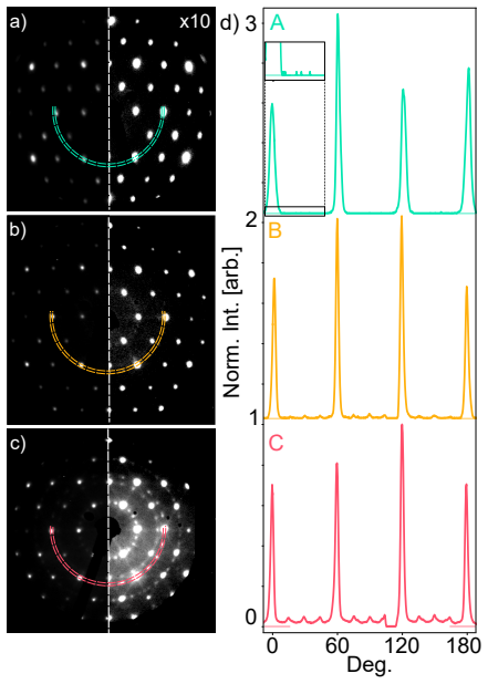
The central discovery is that the exciton lifetime and decay mechanism in C60 thin films change qualitatively when rotational grain boundaries are present, even at concentrations almost invisible to standard characterization. A single-domain film shows monoexponential CT1 decay with an 8.3 ps lifetime, while films with secondary domains require a fast component (0.5-1 ps) and are best described by a two-population model in which one population decays linearly and the other decays via exciton-exciton annihilation, with annihilation rates of 3.3 and 1.3 inverse picoseconds for the two defective films. STM and STS resolve a widened HOMO-LUMO gap localized at the boundary; the authors attribute this to reduced local dielectric screening and argue that, because exciton binding grows as the inverse square of the dielectric constant while the single-particle polarization shift grows only inversely, the two-particle excitonic state is lower in energy at the boundary. They conclude that grain boundaries act as exciton funnels, raising the local exciton density and opening additional decay channels, so precise structural control is required to obtain intrinsic exciton lifetimes.
Load-bearing premise
The load-bearing premise is that the locally reduced dielectric constant at a grain boundary, inferred from widened single-particle STS gaps, is enough to lower the two-particle exciton state and collect nearby excitons; the two-particle states are never measured directly, and the STM film is not the same film used for the TR-ARPES lifetime measurements.
Editorial extensions
If this is right
- A single-domain C60 film shows a single-exponential CT1 decay with an 8.3 ps lifetime; any film with even a few percent of secondary rotational domains requires an additional fast decay component.
- Because the minority domains in the two defective films were only visible in LEED images saturated tenfold, standard unsaturated LEED and static ARPES are insufficient to certify films as boundary-free.
- The two-population model with one linear decay and one exciton-exciton annihilation term fits the defective films better than a bi-exponential, supporting the idea that boundaries localize excitons and raise their local density.
- A grain boundary is expected to act as an exciton funnel because the two-particle state is inferred to be lower in energy there, so nearby excitons migrate toward it and become more likely to collide and annihilate.
- Additional radiative and non-radiative decay channels from relaxed selection rules and modified phonon coupling at the boundary further shorten the observed lifetime.
Reading between the lines
- A clean control the paper does not run: keep a single fixed film and vary pump fluence; a boundary-free film should stay single-exponential at all fluences, while a defective film should show a growing annihilation rate with fluence. The paper varies fluence together with domain fraction, so this test remains open.
- If boundaries funnel excitons as the paper suggests, the same dielectric-mismatch mechanism should apply to other molecular semiconductors with low-dielectric-constant boundaries, making fluence-dependent TR-ARPES a general probe of boundary density.
- The funneling picture implies grain boundaries could be engineered as deterministic exciton collection lines or single-photon emission sites, extending the X-trap analogy from accidental defects to designed structures; that device direction is not demonstrated in the paper.
Signed reviews
Editorial analysis
A structured set of objections, weighed in public.
Referee Report
Summary. The manuscript reports time- and angle-resolved photoemission measurements on three epitaxial C60/Au(111) films with differing rotational-domain content, finding that films with multiple rotational domains show shorter CT1 exciton lifetimes and require an exciton-exciton annihilation term in the decay model. STM/STS across a D1/D2 grain boundary shows a widened single-particle gap, which the authors attribute to a locally reduced dielectric constant; they argue that this lowers the two-particle exciton energy, funneling excitons toward the boundary and enhancing annihilation. The paper thus proposes that even a small proportion of rotational domains, nearly undetectable in unsaturated LEED, can dominate exciton dynamics in organic thin films.
Significance. The central claim is significant for organic optoelectronics because it suggests that minute structural disorder, usually invisible to standard ensemble characterization, can strongly affect exciton lifetimes and create nonlinear decay channels. The paper has several clear strengths: the use of strongly saturated LEED to reveal weak rotational domains is a practical and convincing diagnostic; Sample A, despite having the highest pump fluence, shows no evidence of exciton-exciton annihilation and thereby provides a useful control against fluence-driven effects; the manuscript is transparent about the pump-fluence variation across samples; and the STM maps provide direct spatial evidence of a widened gap at a grain boundary. If the funneling mechanism is confirmed, the work would motivate stricter structural control in OPV materials and could inform the engineering of localized exciton emitters. The empirical observation of lifetime quenching and enhanced two-exciton processes in multi-domain films is, in my assessment, credible and well supported by the A versus B/C comparison.
major comments (4)
- [Eqs. (4)-(6) and the paragraph following Eq. (6)] The assertion that 'for realistic values of a and μ, ΔEB increases more rapidly than ΔEBG' is central to the proposed exciton-funneling mechanism but is not substantiated. The ratio ΔEB/ΔEBG equals (μ/m_e)(a/a0)(1/ε2 + 1/ε1), which depends strongly on the chosen parameters; for example, μ/m_e ≈ 0.1 and a ≈ 0.5 nm gives a ratio near or below unity for typical dielectric constants, which would not support funneling. Please provide the specific values of a and μ used, or a parameter sweep showing the regime in which the two-particle shift dominates, and discuss how those values compare with literature estimates for C60 charge-transfer excitons.
- [Fig. 2, Table 1, and the paragraph discussing pump fluence] The pump fluence and time resolution are not matched across the three samples (350/300/212 µJ/cm² and 470/230/230 fs). While the A versus B/C comparison is controlled in the sense that A has the highest fluence and still shows no annihilation, the quantitative comparison between Samples B and C is confounded: B has a higher fluence and a smaller secondary-domain LEED signal than C, so its larger kExEx (3.3 vs 1.3 ps⁻¹) cannot be unambiguously attributed to a higher grain-boundary density. A matched-fluence measurement of at least two multi-domain samples, or an explicit statement that the B/C comparison is not used to infer a density dependence, is needed to secure the quantitative interpretation of the annihilation rates.
- [Fig. 3 and the STM paragraph in Methods] The STM/STS film was grown by room-temperature deposition to intentionally create grain boundaries, whereas the TR-ARPES films were grown by the two-stage method, and the manuscript does not demonstrate that the D1/D2 grain boundary imaged by STM is representative of the boundaries present in Samples B and C. Since the funneling mechanism is proposed to explain the TR-ARPES results, please provide evidence that the same types of rotational-domain boundaries exist in the TR-ARPES films, or state this as an explicit assumption and discuss its limitations.
- [Eq. (1) and Table 1] For Sample C, the bi-exponential and the exciton-exciton annihilation models yield nearly identical reduced chi-squared values (1.0 vs 0.96), so the data do not uniquely require an annihilation term for that sample. The evidence for EEA therefore rests mainly on Sample B. The manuscript should explicitly acknowledge this model degeneracy rather than implying that both multi-domain samples equally support the EEA mechanism, and should discuss how the additional fluence-dependent data in the supporting information (Fig. S9) helps break this degeneracy.
minor comments (4)
- [Abstract] The phrase 'essential for optimize the performance' should read 'essential for optimizing the performance'.
- [Paragraph after Fig. 2] The sentence 'Sample A measurements are preformed using the highest fluence' contains a typo: 'preformed' should be 'performed'.
- [Eq. (1)] Please define all parameters in Eq. (1) in the main text (A1, A2, τ_rise) and state explicitly that the model is convolved with a Gaussian instrument response, as is done in the text but not in the equation itself.
- [References] Reference 7 writes 'C 60 single crystals' with a space; the spacing of 'C60' is inconsistent in a few places (e.g., reference 20 and the abstract). Please standardize.
Circularity Check
No significant circularity: fitted lifetimes are empirical, and the dielectric-funnel mechanism rests on standard electrostatic formulas rather than on the fitted parameters.
full rationale
Walked the derivation chain: (1) LEED and STM establish that Samples B and C contain additional rotational domains; (2) TR-ARPES decay traces are fit with single-exponential, bi-exponential, and exciton-exciton annihilation models, with model selection based on reduced chi-squared; (3) STS shows a widened transport gap at the grain boundary, interpreted through the classical polarization-energy formulas in Eqs. (2)-(4); (4) Eqs. (5)-(6) are then used to infer that a locally reduced dielectric constant increases the exciton binding energy more than the single-particle gap, leading to the proposed exciton-funnel mechanism. None of these steps defines its output in terms of its input, and no fitted parameter is renamed as a prediction: the decay rates k and k_ExEx are extracted from the time traces, while the dielectric-funnel claim is derived from standard electrostatics with stated, if not numerically pinned down, parameters a and mu. The paper contains self-citations, including the two-stage growth recipe (Ref. 11), polarization-induced level shifts (Ref. 24), and the laser-based TR-ARPES apparatus (Ref. 30), but these are experimental or methodological results that are externally grounded and are not used as a uniqueness theorem to force the paper's interpretation. The acknowledged unmatched pump fluences (350, 300, and 212 uJ/cm^2 for Samples A, B, and C) and the fact that two-particle excitonic states are inferred from single-particle STS rather than measured directly are genuine limitations of experimental comparability and evidence strength, but they are confounds or indirectness, not circularity. No equation-level reduction of the claimed result to its own inputs can be exhibited, so the appropriate finding is no significant circularity.
Assumptions & free parameters
free parameters (3)
- Linear decay rate k =
0.127 ± 0.006 ps⁻¹ (Sample B); 0.07 ± 0.02 ps⁻¹ (Sample C)
- Exciton-exciton annihilation rate kExEx =
3.3 ± 0.2 ps⁻¹ (Sample B); 1.3 ± 0.1 ps⁻¹ (Sample C)
- Polarization radius a and reduced exciton mass μ =
Not specified; described as realistics values
assumptions (5)
- domain assumption Classical polarization energy formula P = (e²/2a)(1-1/ε) (Eq. 3) and resulting gap scaling (Eq. 4) apply at the grain boundary.
- domain assumption Hydrogenic exciton binding energy EB = μe⁴/(2(4πε0εℏ)²) (Eq. 5) applies to C60 CT1 excitons and to the grain-boundary region.
- ad hoc to paper The grain boundary imaged by STM (D1/D2, Fig. 3) is representative of the grain boundaries present in TR-ARPES Samples B and C.
- ad hoc to paper Exciton decay in multi-domain films is described by two independent populations: a linear-decay population and an annihilation-decay population (Eq. 1).
- domain assumption Sample A is a sufficient single-domain reference for the intrinsic exciton lifetime.
Cite this review
Pith. "Pith review of Quenching of excitons at grain boundaries in C60 thin films." pith.science (2026). https://pith.science/paper/AYCJBZ6U
@misc{pith2026250700323,
  author       = {Pith},
  title        = {Pith review of: Quenching of excitons at grain boundaries in C60 thin films},
  year         = {2026},
  howpublished = {\url{https://pith.science/paper/AYCJBZ6U}},
  note         = {Machine review of arXiv:2507.00323}
}
read the original abstract
Exciton lifetimes play a critical role in the performance of organic optoelectronic devices. In this work, we investigate how the presence of multiple rotational domains, and therefore grain boundaries, impacts exciton dynamics in thin films of C60/Au(111) using time and angle-resolved photoemission spectroscopy (TR-ARPES). We find that films with multiple rotational domains exhibit shorter exciton lifetimes and evidence of exciton-exciton annihilation, even when one domain predominates. Scanning tunneling microscopy (STM) measurements reveal electronic structure changes resulting from a locally reduced dielectric constant at grain boundaries, providing a mechanism for lifetime reduction through exciton funneling and other additional decay channels. These findings highlight the critical role of film quality in determining intrinsic exciton lifetimes, and show that minuscule amounts of disorder that are nearly undetectable by ensemble measurements can significantly impact dynamics. These results imply that precise structural control is essential for optimize the performance of organic optoelectronic devices.
Figures

Figures from the paper (1 more)

Reference graph
Works this paper leans on
-
[1]
M. Pelzer, K.; B. Darling, S. Charge generation in organic photovoltaics: a review of theory and computation. Molecular Systems Design & Engineering 2016, 1, 10--24, Publisher: Royal Society of Chemistry
work page 2016
-
[2]
V. Mikhnenko, O.; M. Blom, P. W.; Nguyen, T.-Q. Exciton diffusion in organic semiconductors. Energy & Environmental Science 2015, 8, 1867--1888, Publisher: Royal Society of Chemistry
work page 2015
-
[3]
Terao, Y.; Sasabe, H.; Adachi, C. Correlation of hole mobility, exciton diffusion length, and solar cell characteristics in phthalocyanine/fullerene organic solar cells. Applied Physics Letters 2007, 90, 103515
work page 2007
-
[4]
C.; Hwang, J.; Suijkerbuijk, J
Fravventura, M. C.; Hwang, J.; Suijkerbuijk, J. W. A.; Erk, P.; Siebbeles, L. D. A.; Savenije, T. J. Determination of Singlet Exciton Diffusion Length in Thin Evaporated C60 Films for Photovoltaics . J. Phys. Chem. Lett. 2012, 3, 2367--2373, Publisher: American Chemical Society
work page 2012
-
[5]
Lunt, R. R.; Benziger, J. B.; Forrest, S. R. Relationship between Crystalline Order and Exciton Diffusion Length in Molecular Organic Semiconductors . Advanced Materials 2010, 22, 1233--1236, \_eprint: https://onlinelibrary.wiley.com/doi/pdf/10.1002/adma.200902827
-
[6]
Sajjad, M. T.; Ward, A. J.; Kästner, C.; Ruseckas, A.; Hoppe, H.; Samuel, I. D. W. Controlling Exciton Diffusion and Fullerene Distribution in Photovoltaic Blends by Side Chain Modification . J. Phys. Chem. Lett. 2015, 6, 3054--3060, Publisher: American Chemical Society
work page 2015
-
[7]
O.; Taliani, C.; Mohn, H.; Müller, W.; Häussler, P.; Ter Meer, H.-U
Guss, W.; Feldmann, J.; Göbel, E. O.; Taliani, C.; Mohn, H.; Müller, W.; Häussler, P.; Ter Meer, H.-U. Fluorescence from X traps in C 60 single crystals. Phys. Rev. Lett. 1994, 72, 2644--2647
work page 1994
-
[8]
Merino, P.; Große, C.; Rosławska, A.; Kuhnke, K.; Kern, K. Exciton dynamics of C60 -based single-photon emitters explored by Hanbury Brown – Twiss scanning tunnelling microscopy. Nat Commun 2015, 6, 8461, Publisher: Nature Publishing Group
work page 2015
Show all 32 references
-
[9]
C.; Gunnarsson, O.; Etzkorn, M.; Kuhnke, K.; Kern, K
Rosławska, A.; Merino, P.; Große, C.; Leon, C. C.; Gunnarsson, O.; Etzkorn, M.; Kuhnke, K.; Kern, K. Single Charge and Exciton Dynamics Probed by Molecular - Scale - Induced Electroluminescence . Nano Lett. 2018, 18, 4001--4007, Publisher: American Chemical Society
2018
-
[10]
Nanoscale Imaging of Charge Carrier and Exciton Trapping at Structural Defects in Organic Semiconductors
Große, C.; Gunnarsson, O.; Merino, P.; Kuhnke, K.; Kern, K. Nanoscale Imaging of Charge Carrier and Exciton Trapping at Structural Defects in Organic Semiconductors . Nano Lett. 2016, 16, 2084--2089
2016
-
[11]
Tully, A. B. et al. Two- Stage Growth for Highly Ordered Epitaxial C60 Films on Au (111). J. Phys. Chem. C 2024, 128, 18128--18134, Publisher: American Chemical Society
2024
-
[12]
On interface dipole layers between C 60 and Ag or Au
Veenstra, S.; Heeres, A.; Hadziioannou, G.; Sawatzky, G.; Jonkman, H. On interface dipole layers between C 60 and Ag or Au . Applied Physics A: Materials Science & Processing 2002, 75, 661--666
2002
-
[13]
H.; Hesper, R.; Heessels, A
Tjeng, L. H.; Hesper, R.; Heessels, A. C. L.; Heeres, A.; Jot, H. T. DEVELOPMENT OF THE ELECTRONIC STRUCTURE IN A K - DOPED Cc0 MONOLAYER ON A Ag (1 1 1) SURFACE . Solid State Commun. 1997, 103, 31 -- 35
1997
-
[14]
Man, P.; Srolovitz, D.; Zhao, J.; Ly, T. H. Functional Grain Boundaries in Two - Dimensional Transition - Metal Dichalcogenides . Acc. Chem. Res. 2021, 54, 4191--4202, Publisher: American Chemical Society
2021
-
[15]
S.; Yun, S
Kim, M. S.; Yun, S. J.; Lee, Y.; Seo, C.; Han, G. H.; Kim, K. K.; Lee, Y. H.; Kim, J. Biexciton Emission from Edges and Grain Boundaries of Triangular WS _ 2 Monolayers . ACS Nano 2016, 10, 2399--2405
2016
-
[16]
Kim, H. W. Recent progress in the role of grain boundaries in two-dimensional transition metal dichalcogenides studied using scanning tunneling microscopy/spectroscopy. Appl. Microsc. 2023, 53, 5
2023
-
[17]
Exciton physics and device application of two-dimensional transition metal dichalcogenide semiconductors
Mueller, T.; Malic, E. Exciton physics and device application of two-dimensional transition metal dichalcogenide semiconductors. npj 2D Mater Appl 2018, 2, 29
2018
-
[18]
D.; McCreary, K
Cunningham, P. D.; McCreary, K. M.; Hanbicki, A. T.; Currie, M.; Jonker, B. T.; Hayden, L. M. Charge Trapping and Exciton Dynamics in Large - Area CVD Grown MoS2 . J. Phys. Chem. C 2016, 120, 5819--5826, Publisher: American Chemical Society
2016
-
[19]
G.; Jung, G
Zhou, Y.; Sarwat, S. G.; Jung, G. S.; Buehler, M. J.; Bhaskaran, H.; Warner, J. H. Grain Boundaries as Electrical Conduction Channels in Polycrystalline Monolayer WS2 . ACS Appl. Mater. Interfaces 2019, 11, 10189--10197, Publisher: American Chemical Society
2019
-
[20]
A.; Castellanos-Gomez, A.; Zant, H
Tonndorf, P.; Schmidt, R.; Schneider, R.; Kern, J.; Buscema, M.; Steele, G. A.; Castellanos-Gomez, A.; Zant, H. S. J. v. d.; Vasconcellos, S. M. d.; Bratschitsch, R. Single-photon emission from localized excitons in an atomically thin semiconductor. Optica, OPTICA 2015, 2, 347...
2015
-
[21]
Ultrafast Charge - Transfer Exciton Dynamics in C _ 60 Thin Films
Emmerich, S.; Hedwig, S.; Arnoldi, B.; Stöckl, J.; Haag, F.; Hemm, R.; Cinchetti, M.; Mathias, S.; Stadtmüller, B.; Aeschlimann, M. Ultrafast Charge - Transfer Exciton Dynamics in C _ 60 Thin Films . J. Phys. Chem. C 2020, 124, 23579--23587
2020
-
[22]
Bennecke, W. et al. Disentangling the multiorbital contributions of excitons by photoemission exciton tomography. Nat Commun 2024, 15, 1804, Publisher: Nature Publishing Group
2024
-
[23]
Strong modification of the transport level alignment in organic materials after optical excitation
Stadtmüller, B.; Emmerich, S.; Jungkenn, D.; Haag, N.; Rollinger, M.; Eich, S.; Maniraj, M.; Aeschlimann, M.; Cinchetti, M.; Mathias, S. Strong modification of the transport level alignment in organic materials after optical excitation. Nat Commun 2019, 10, 1470
2019
-
[24]
A.; Schiffrin, A.; Roussy, T
Cochrane, K. A.; Schiffrin, A.; Roussy, T. S.; Capsoni, M.; Burke, S. A. Pronounced polarization-induced energy level shifts at boundaries of organic semiconductor nanostructures. Nat Commun 2015, 6, 8312, Publisher: Nature Publishing Group
2015
-
[25]
Y.; Wu, H.; Cotts, B
Sharifzadeh, S.; Wong, C. Y.; Wu, H.; Cotts, B. L.; Kronik, L.; Ginsberg, N. S.; Neaton, J. B. Relating the Physical Structure and Optoelectronic Function of Crystalline TIPS - Pentacene . Advanced Functional Materials 2015, 25, 2038--2046, \_eprint: https://onlinelibrary.wile...
2015 doi
-
[26]
J.; Munn, R
Bounds, P. J.; Munn, R. W. Polarization energy of a localized charge in a molecular crystal. Chemical Physics 1979, 44, 103--112
1979
-
[27]
V.; Soos, Z
Tsiper, E. V.; Soos, Z. G. Charge redistribution and polarization energy of organic molecular crystals. Phys. Rev. B 2001, 64, 195124
2001
-
[28]
V.; Soos, Z
Tsiper, E. V.; Soos, Z. G. Electronic polarization in pentacene crystals and thin films. Phys. Rev. B 2003, 68, 085301, arXiv:cond-mat/0303556
2003 arXiv
-
[29]
F.; Schöneboom, J
Rim, S.-B.; Fink, R. F.; Schöneboom, J. C.; Erk, P.; Peumans, P. Effect of molecular packing on the exciton diffusion length in organic solar cells. Applied Physics Letters 2007, 91, 173504
2007
-
[30]
Dufresne, S. K. Y.; Zhdanovich, S.; Michiardi, M.; Guislain, B. G.; Zonno, M.; Mazzotti, V.; O’Brien, L.; Kung, S.; Levy, G.; Mills, A. K.; Boschini, F.; Jones, D. J.; Damascelli, A. A versatile laser-based apparatus for time-resolved ARPES with micro-scale spatial resolution....
2024
-
[31]
I.; Colton, J
Altman, E. I.; Colton, J. Nucleation, growth, and structure of fullerene films on Au ( 111). Surf. Sci. 1992, 279, 29 -- 67
1992
-
[32]
C+ 5moׇT h#ec1 v;n/ |)_c 'EklsZʄoC Evv eT ,fOD;f JԌ楷66wn1Q0E h* hS`Ouu 2ȧ 8 _K | M է [ l1 !
Gardener, J. A.; Briggs, G. A. D.; Castell, M. R. Scanning tunneling microscopy studies of C60 monolayers on Au (111). Phys. Rev. B 2009, 80, 235434, Publisher: American Physical Society mcitethebibliography main__2_.tex0000664000000000000000000015412015030617276011755 0ustar ...
2009
Reviewed August 6, 2026 · model on record in the stance chip above.
Discussion (0). Continue with ORCID to comment.