REVIEW 3 major objections 5 minor 69 references
Deep Learning-based Multi Project InP Wafer Simulation for Unsupervised Surface Defect Detection
T0 review · 3 major / 5 minor · reviewed 2026-08-07 · deepseek-v4-flash
Pith's one-line read Defect-free 'golden die' simulated from CAD plans by a U-Net
desk verdict A credible applied U-Net for simulating defect-free InP wafers from CAD, but the core claim of defect-free output is not actually measured with the pixel-perfect labels the authors made. read the letter →
The pith
A machine-rendered reading of the paper's core claim, the machinery that carries it, and where it could break.
The reading
What carries the argument
The central object is the U-Net (an encoder-decoder fully convolutional network with skip connections) that maps a stack of binary CAD layer bitmaps to either RGB pixel values (regression) or per-pixel class scores over a 64-color quantized palette (classification). The skip connections align input and output structures, letting the network transfer CAD geometry into the photograph domain; the training objective is a dissimilarity measure between the simulated and real patches, and the same measures (L2, LPIPS, etc.) are later used as similarity metrics to generate defect score maps. The paper also uses variance-thresholded patch sampling to focus training on informative regions, and a per-wafer model because each wafer run has distinct visual characteristics.
What would settle it
Train the same U-Net on a synthetic wafer with pixel-perfect defect labels and deliberately high defect density covering a large fraction of the CAD features; if the simulator then reconstructs the defects or fails to localize them in the score map, the sparsity assumption is broken. Alternatively, inspect simulations on real wafers for hallucinated structures not present in the CAD layers, which the paper itself already observes in some LPIPS-trained models.
Extended reading notes
Core claim
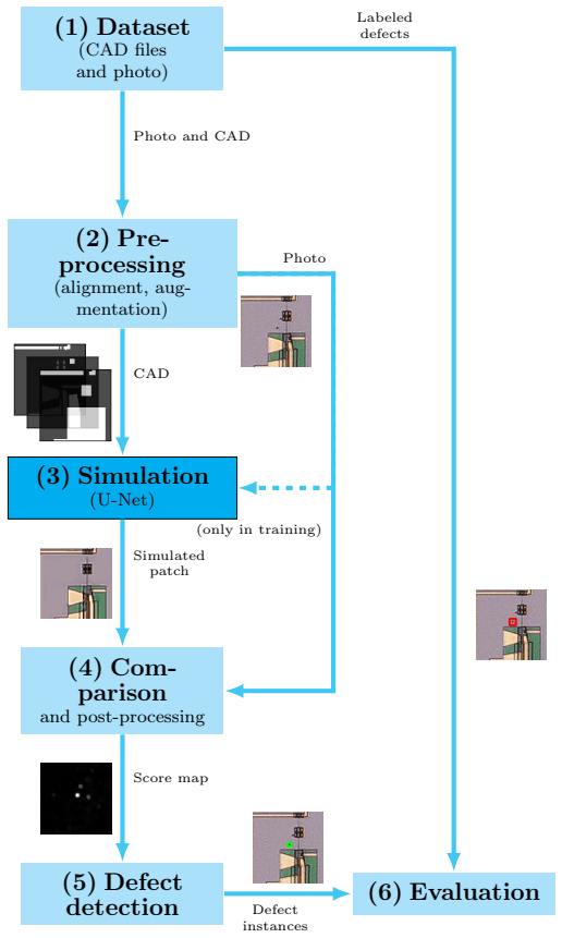
The central claim is that a fully convolutional U-Net, fed with binary CAD manufacturing layers, can predict a photorealistic, defect-free wafer photograph even when the training target photographs contain unlabeled defects. Because defects are sparse relative to CAD-correlated structures, the network learns the regular process appearance rather than copying the anomalies, and the resulting simulation can be used as a golden standard for template-matching defect detection. The paper evaluates four training objectives—regression with L2 and LPIPS, classification with cross-entropy and focal loss—and finds all outperform a decision-tree baseline, with semantic segmentation on quantized color palettes giving the most consistent results. The authors report that the defect-free property holds even for a wafer with unusually high defect density, and that the generated golden die enables defect localization via pixelwise similarity scores, though simulation hallucinations and CAD-to-photo misalignment remain failure modes.
Load-bearing premise
The load-bearing premise is that manufacturing defects are rare enough and visually separable enough from the CAD-defined structures that the U-Net will learn the clean wafer appearance rather than reproducing the defects.
Editorial extensions
If this is right
- Golden standards can be generated from CAD plans for multi-project wafer runs where no physical defect-free die exists.
- Defect detection becomes possible on any user-defined wafer region without any labeled defect data.
- The same simulation approach could monitor intermediate manufacturing steps, since CAD layers correspond to individual process steps.
- Training is fast relative to the months-long manufacturing cycle, so the pipeline could run on modest or embedded hardware in a foundry.
- Dissimilarity maps between simulation and photo can guide human annotation, cutting the roughly 20 hours per wafer that manual inspection currently requires.
Reading between the lines
- Editorial inference: the sparsity assumption could be tested directly on the released synthetic data by training on high-defect-density variants and checking whether the simulator systematically reproduces defects, an experiment the paper does not run.
- Editorial inference: the method likely transfers to other structured-manufacturing domains where CAD or layout plans coexist with surface images, such as PCB or MEMS fabrication, because the same sparse-anomaly-plus-strong-structural-prior condition holds there.
- Editorial inference: using a perceptual loss like LPIPS improves simulated noise realism but may hurt defect detection because the photo noise is reproduced as structure; a task-specific objective that penalizes structure hallucination could be more useful than purely perceptual fidelity.
Editorial analysis
A structured set of objections, weighed in public.
Referee Report
Summary. The paper proposes a U-Net-based method that takes CAD layer bitmaps as input and predicts wafer photographs, with the goal of producing a defect-free "simulated golden die" for template-matching-based defect detection on InP multi-project wafers. The authors train classification and regression variants with four training objectives on five synthetic datasets and nine real wafer datasets, compare them against decision-tree baselines, and evaluate simulation quality with similarity metrics in RGB and quantized color space. They also demonstrate a defect-detection workflow using pixelwise dissimilarity score maps. The central claim is that models trained on defective wafer photographs yield defect-free simulations that can serve as golden standards for unsupervised inspection.
Significance. If the central claim were established, the method would be practically valuable for InP multi-project wafer manufacturing, where golden standards are typically unavailable and manual inspection is costly. The paper has notable strengths: it introduces synthetic wafer datasets with pixel-perfect defect labels, trains a large set of models (167 models) across four objectives, provides extensive similarity-metric tables and correlation analyses, and honestly reports failure modes such as hallucinations. However, the key claim that the simulator removes defects rather than memorizing them is not quantitatively supported. All reported similarity metrics compare simulations to the defective target photographs, and the available pixel-perfect labels on the synthetic datasets are never used for the load-bearing validation. The result is therefore promising but not yet demonstrated.
major comments (3)
- [Section 3.2, Section 3.3, Appendix A] The quantitative evidence for defect-free simulation is missing. All reported metrics (L2, LPIPS, PSNR, cross-entropy, k-off) compare the simulation to the actual wafer photograph, which contains defects, and the "best" checkpoints are selected by L2 and LPIPS against that same defective ground truth (Section 3.2). A model that faithfully reproduces defects would receive good scores under this protocol, and Section 3.3 explicitly notes that models tend to rank better when evaluated with their own training objective. The pixel-perfect defect labels on S1-S5 are never used to measure whether defects are removed. I request a defect-reproduction analysis on the synthetic datasets: for example, report the fraction of labeled defect pixels that produce a high dissimilarity in the simulation, or the precision/recall of the simulation-vs-photo difference at the labeled defect masks, separately from non-defective background. This is the load-bearing test for the Conclusion's claim that "even when utilizing defective wafers as simulation targets, the trained models yield defect-free simulations."
- [Section 4] The defect-detection results are anecdotal. Only two patches are quantified (AP 0.98 in Figure 20 and AP 0.44 in Figure 21), and no aggregate average precision is reported over the validation split or across the five synthetic datasets with pixel-perfect labels. The statement that "automated defect detection by template matching in synthetic data is virtually perfect when the simulation is good enough" is therefore not supported by the presented evidence. Please report the mean and standard deviation of AP over all validation patches and datasets, ideally per defect class, and state the exact thresholding protocol used to binarize the score map.
- [Section 4, Figure 21] Hallucinations are reported as a known failure mode, but their frequency and impact are not quantified. The paper states that defect detection "fails completely when there is an anomaly in the simulated patch" and shows hallucinations generating false positives; this is the opposite failure mode of a defect-free golden die and directly threatens the central premise. Please quantify hallucination incidence (for example, the fraction of simulated patches containing artifacts and the total hallucinated area) and report detection AP both including and excluding hallucinated patches, or propose and evaluate a post-processing mechanism that identifies and rejects such patches.
minor comments (5)
- [Section 3.1 vs. Appendix B] The training configuration is internally inconsistent: Section 3.1 specifies SGD with an initial learning rate of 5e-3 and a multiplicative decay schedule, while Appendix B states that the optimizer was Adam with learning rate 1e-4 (beta1=0.9, beta2=0.999) and that a batch size of 32 was chosen, whereas Section 3.1 says batches have at most 128 patches. Please specify the exact optimizer, learning-rate schedule, batch size, and variance threshold used for each reported model so that the 167 models can be reproduced.
- [Section 1] The sentence "In Section 4 outlines a pathway for template matching-based defect detection using our simulations" is ungrammatical; it should read "Section 4 outlines" or "In Section 4 we outline".
- [Section 3.1] "We disconsider samples" is not standard English; use "discard" or "exclude".
- [Section 2] The sentence describing the synthetic datasets says they are "square images of 10k×10k pixels," but Figure D.25 shows a sample described as 2000×2667 pixels; please clarify whether the 10k×10k size refers to the full wafer image from which patches are extracted.
- [Appendix B] The variance-threshold values are reported only for a subset of models ("R2 on LPIPS (v=20)", "R3, R5 and R8 on LPIPS (v=0, 30 epochs)", etc.), but not for all models; a complete table of hyperparameters per dataset and objective would improve reproducibility.
Circularity Check
Mild circularity from checkpoint selection by the same L2/LPIPS metrics later reported as evidence; the central defect-free claim rests on an unverified expectation rather than a circular derivation.
-
fitted input called prediction
[Section 3.2 (Evaluation methodology) and Section 3.3 (Results)]
"We present results for the models generated after the 10-th training epoch and for the best performing intermediate checkpoints. We select a set of best models according to the MSE similarity to the ground truth and a set of checkpoints based on their LPIPS performance."
The 'best' checkpoint is selected on the validation split using the same L2/LPIPS metrics that are subsequently reported as evidence of simulation quality and used to rank models against the decision-tree baseline. By construction, the reported 'best epoch' L2/LPIPS value is the minimum over the evaluated checkpoints for that metric, while the decision tree is given no equivalent epoch-selection step; hence the claimed U-Net outperformance is partly a restatement of the selection rule rather than an independent prediction. The paper itself concedes that 'models tend to perform better when evaluated on the same function used as a training objective,' confirming that the metric ranking is confounded with the selection criterion.
full rationale
The core pipeline is not circular: the U-Net is trained to map CAD layer bitmaps to photographed wafer appearance, and the decision-tree baseline is a legitimate comparator apart from the checkpoint-selection bias. No load-bearing self-citation or imported-uniqueness argument appears; prior theses by the authors are cited only for alignment, quantization, and annotation details. The central weakness is that the 'defect-free golden die' claim is supported by qualitative samples and by similarity scores computed against defective ground-truth images, which cannot by themselves establish that defects were removed rather than memorized; this is a validity gap, not a definitional or self-citational circularity. The one genuine circular element is the overlap between the L2/LPIPS checkpoint-selection criterion and the L2/LPIPS evaluation, which is partial, acknowledged by the authors, and does not force the central conclusion by itself.
Assumptions & free parameters
free parameters (5)
- Color palette size k =
64
- Variance threshold v for patch filtering =
0 to 50 (per dataset)
- Batch size =
32
- Learning rate and optimizer =
SGD 5e-3 with decay in Section 3.1; Adam 1e-4 in Appendix B
- Best epoch checkpoint =
10th epoch or best validation L2/LPIPS
assumptions (3)
- domain assumption The visual appearance of the wafer is determined by the CAD layers, so a function g -> p exists and is learnable.
- domain assumption Manufacturing defects are sparse enough that a capacity-limited network will not systematically reproduce them in its output.
- standard math The U-Net with three downsampling stages can represent the wafer appearance function at 64x64 patch resolution.
Cite this review
Pith. "Pith review of Deep Learning-based Multi Project InP Wafer Simulation for Unsupervised Surface Defect Detection." pith.science (2026). https://pith.science/paper/BXDP34NX
@misc{pith2026250610713,
  author       = {Pith},
  title        = {Pith review of: Deep Learning-based Multi Project InP Wafer Simulation for Unsupervised Surface Defect Detection},
  year         = {2026},
  howpublished = {\url{https://pith.science/paper/BXDP34NX}},
  note         = {Machine review of arXiv:2506.10713}
}
read the original abstract
Quality management in semiconductor manufacturing often relies on template matching with known golden standards. For Indium-Phosphide (InP) multi-project wafer manufacturing, low production scale and high design variability lead to such golden standards being typically unavailable. Defect detection, in turn, is manual and labor-intensive. This work addresses this challenge by proposing a methodology to generate a synthetic golden standard using Deep Neural Networks, trained to simulate photo-realistic InP wafer images from CAD data. We evaluate various training objectives and assess the quality of the simulated images on both synthetic data and InP wafer photographs. Our deep-learning-based method outperforms a baseline decision-tree-based approach, enabling the use of a 'simulated golden die' from CAD plans in any user-defined region of a wafer for more efficient defect detection. We apply our method to a template matching procedure, to demonstrate its practical utility in surface defect detection.
Figures


Figures from the paper (20 more)


Reference graph
Works this paper leans on
-
[1]
Unsupervised pixel-wise hyperspectral anomaly detection via autoencoding adversarial networks
Arisoy, S., Nasrabadi, N.M., Kayabol, K., 2021. Unsupervised pixel-wise hyperspectral anomaly detection via autoencoding adversarial networks. IEEE Geoscience and Remote Sensing Letters 19, 1–5
work page 2021
-
[2]
Barone, M., 2020. Robust Image Wafer Inspection, in: 2020 Tenth International Conference on Image Processing Theory, Tools and Appli- cations (IPTA), IEEE. pp. 1–6
work page 2020
-
[3]
Bati, E., Çalışkan, A., Koz, A., Alatan, A.A., 2015. Hyperspectral anomaly detection method based on auto-encoder, in: Image and Signal Processing for Remote Sensing XXI, Spie. pp. 220–226
work page 2015
-
[4]
Bennett, M.H., Tobin Jr, K.W., Gleason, S.S., 1995. Automatic defect classification: status and industry trends, in: Integrated Circuit Metrol- ogy, Inspection, and Process Control IX, SPIE. pp. 210–220
work page 1995
-
[5]
Image-based surface defect detection using deep learning: A review
Bhatt, P.M., Malhan, R.K., Rajendran, P., Shah, B.C., Thakar, S., Yoon, Y.J., Gupta, S.K., 2021. Image-based surface defect detection using deep learning: A review. Journal of Computing and Information Science in Engineering 21
work page 2021
-
[6]
Wafer Defect Inspection by Neural Analysis of Region Features
Chang, C.Y., Li, C.H., Chang, Y.C., Jeng, M., 2011. Wafer Defect Inspection by Neural Analysis of Region Features. Journal of Intelligent Manufacturing 22, 953–964. 28
work page 2011
-
[7]
Application of two Hopfield Neural Networks for Automatic four-element LED Inspection
Chang, C.Y., Li, C.H., Lin, S.Y., Jeng, M., 2009. Application of two Hopfield Neural Networks for Automatic four-element LED Inspection. IEEE Transactions on Systems, Man, and Cybernetics, Part C (Appli- cations and Reviews) 39, 352–365
work page 2009
-
[8]
Chapelle, O., Scholkopf, B., Zien, A., 2006. Semi-supervised learning
work page 2006
Show all 69 references
-
[9]
A Neural-Network Approach to Recognize DefectSpatialPatterninSemiconductorFabrication
Chen, F.L., Liu, S.F., 2000. A Neural-Network Approach to Recognize DefectSpatialPatterninSemiconductorFabrication. IEEEtransactions on semiconductor manufacturing 13, 366–373
2000
-
[10]
A Neural-Network Approach for an Au- tomatic LED Inspection System
Chen, W.C., Hsu, S.W., 2007. A Neural-Network Approach for an Au- tomatic LED Inspection System. Expert Systems with Applications 33, 531–537
2007
-
[11]
A light-weighted cnn model for wafer structural defect detection
Chen, X., Chen, J., Han, X., Zhao, C., Zhang, D., Zhu, K., Su, Y., 2020. A light-weighted cnn model for wafer structural defect detection. IEEE access 8, 24006–24018
2020
-
[12]
Convolutional neu- ral network for wafer surface defect classification and the detection of unknown defect class
Cheon, S., Lee, H., Kim, C.O., Lee, S.H., 2019. Convolutional neu- ral network for wafer surface defect classification and the detection of unknown defect class. IEEE Transactions on Semiconductor Manufac- turing 32, 163–170
2019
-
[13]
Automated visual inspection: A survey
Chin, R.T., Harlow, C.A., 1982. Automated visual inspection: A survey. IEEE transactions on pattern analysis and machine intelligence , 557– 573
1982
-
[14]
Implementation of Reflected Light Die-to-Die Inspection and ReviewSmart to Improve 65nm DRAM Mask Fabrication, in: 25th Annual BACUS Symposium on Photomask Technology, SPIE
Cho, W.I., Park, J.H., Chung, D.H., Cha, B.C., Choi, S.W., Han, W.S., Park, K.H., Kim, N.W., Hess, C., Ma, W., et al., 2005. Implementation of Reflected Light Die-to-Die Inspection and ReviewSmart to Improve 65nm DRAM Mask Fabrication, in: 25th Annual BACUS Symposium on Photom...
2005
-
[15]
Chou, P.B., Rao, A.R., Sturzenbecker, M.C., Wu, F.Y., Brecher, V.H.,
-
[16]
Çiçek, Ö., Abdulkadir, A., Lienkamp, S.S., Brox, T., Ronneberger, O.,
-
[17]
An image-based pipeline for defect local- ization in photonic InP multi-project wafers
Dolgener Cantú, E., 2023. An image-based pipeline for defect local- ization in photonic InP multi-project wafers. Master’s thesis. Tech- nische Universität Berlin. URL:https://doi.org/10.5281/zenodo. 15230127, doi:10.5281/zenodo.15230127
2023 doi
-
[18]
Recent advances in the automatic in- spection of integrated circuits for pattern defects
Dom, B.E., Brecher, V., 1995. Recent advances in the automatic in- spection of integrated circuits for pattern defects. Machine Vision and Applications 8, 5–19
1995
-
[19]
Age and gender estimation of unfiltered faces
Eidinger, E., Enbar, R., Hassner, T., 2014. Age and gender estimation of unfiltered faces. IEEE Transactions on information forensics and security 9, 2170–2179
2014
-
[20]
Unsuper- vised fabric defect detection based on a deep convolutional generative adversarial network
Hu, G., Huang, J., Wang, Q., Li, J., Xu, Z., Huang, X., 2020. Unsuper- vised fabric defect detection based on a deep convolutional generative adversarial network. Textile Research Journal 90, 247–270
2020
-
[21]
Runet: A robust unet architecture for image super-resolution, in: Proceedings of the IEEE/CVF Conference on Computer Vision and Pattern Recog- nition Workshops, pp
Hu, X., Naiel, M.A., Wong, A., Lamm, M., Fieguth, P., 2019. Runet: A robust unet architecture for image super-resolution, in: Proceedings of the IEEE/CVF Conference on Computer Vision and Pattern Recog- nition Workshops, pp. 0–0
2019
-
[22]
Huang, G., Laradji, I., Vazquez, D., Lacoste-Julien, S., Rodriguez, P.,
-
[23]
Automated visual inspection in the semi- conductor industry: A survey
Huang, S.H., Pan, Y.C., 2015. Automated visual inspection in the semi- conductor industry: A survey. Computers in industry 66, 1–10
2015
-
[24]
A cnn-based transfer learning method for defect classification in semiconductor man- ufacturing, in: 2018 international symposium on semiconductor manu- facturing (ISSM), IEEE
Imoto, K., Nakai, T., Ike, T., Haruki, K., Sato, Y., 2018. A cnn-based transfer learning method for defect classification in semiconductor man- ufacturing, in: 2018 international symposium on semiconductor manu- facturing (ISSM), IEEE. pp. 1–3. 30
2018
-
[25]
Batch normalization: Accelerating deep network training by reducing internal covariate shift, in: International conference on machine learning, pmlr
Ioffe, S., Szegedy, C., 2015. Batch normalization: Accelerating deep network training by reducing internal covariate shift, in: International conference on machine learning, pmlr. pp. 448–456
2015
-
[26]
Image-to-image transla- tion with conditional adversarial networks, in: Proceedings of the IEEE conference on computer vision and pattern recognition, pp
Isola, P., Zhu, J.Y., Zhou, T., Efros, A.A., 2017. Image-to-image transla- tion with conditional adversarial networks, in: Proceedings of the IEEE conference on computer vision and pattern recognition, pp. 1125–1134
2017
-
[27]
Color image generation from lidar reflection data by using selected connection unet
Kim, H.K., Yoo, K.Y., Jung, H.Y., 2020. Color image generation from lidar reflection data by using selected connection unet. Sensors 20, 3387
2020
-
[28]
Novel method for detection of mixed-type defect patterns in wafer maps based on a single shot detector algorithm
Kim, T.S., Lee, J.W., Lee, W.K., Sohn, S.Y., 2022. Novel method for detection of mixed-type defect patterns in wafer maps based on a single shot detector algorithm. Journal of Intelligent Manufacturing 33, 1715– 1724
2022
-
[29]
System-on- chip photonic integrated circuits
Kish, F., Lal, V., Evans, P., Corzine, S.W., Ziari, M., Butrie, T., Reffle, M., Tsai, H.S., Dentai, A., Pleumeekers, J., et al., 2017. System-on- chip photonic integrated circuits. IEEE Journal of Selected Topics in Quantum Electronics 24, 1–20
2017
-
[30]
Kohlberger, T., Singh, V., Alvino, C., Bahlmann, C., Grady, L., 2012. Evaluating segmentation error without ground truth, in: Medical Image Computing and Computer-Assisted Intervention–MICCAI 2012: 15th International Conference, Nice, France, October 1-5, 2012, Proceedings, Pa...
2012
-
[31]
Epitaxial growth and layer-transfer techniques for heterogeneous integration of materials for electronic and photonic devices
Kum, H., Lee, D., Kong, W., Kim, H., Park, Y., Kim, Y., Baek, Y., Bae, S.H., Lee, K., Kim, J., 2019. Epitaxial growth and layer-transfer techniques for heterogeneous integration of materials for electronic and photonic devices. Nature Electronics 2, 439–450
2019
-
[32]
Wavelet-baseddefectdetectioninsolarwafer images with inhomogeneous texture
Li, W.C., Tsai, D.M., 2012. Wavelet-baseddefectdetectioninsolarwafer images with inhomogeneous texture. Pattern Recognition 45, 742–756
2012
-
[33]
Concealed object segmenta- tion in terahertz imaging via adversarial learning
Liang, D., Pan, J., Yu, Y., Zhou, H., 2019. Concealed object segmenta- tion in terahertz imaging via adversarial learning. Optik 185, 1104–1114
2019
-
[34]
Foundry 31 capabilities for photonic integrated circuits, in: Optical Fiber Telecom- munications VII
Liehr, M., Baier, M., Hoefler, G., Fahrenkopf, N.M., Bowers, J., Glad- hill, R., O’Brien, P., Timurdogan, E., Su, Z., Kish, F., 2020. Foundry 31 capabilities for photonic integrated circuits, in: Optical Fiber Telecom- munications VII. Elsevier, pp. 143–193
2020
-
[35]
Focal loss for dense object detection, in: Proceedings of the IEEE international conference on computer vision, pp
Lin, T.Y., Goyal, P., Girshick, R., He, K., Dollár, P., 2017. Focal loss for dense object detection, in: Proceedings of the IEEE international conference on computer vision, pp. 2980–2988
2017
-
[36]
Defect detec- tion of ic wafer based on spectral subtraction
Liu, H., Zhou, W., Kuang, Q., Cao, L., Gao, B., 2010. Defect detec- tion of ic wafer based on spectral subtraction. IEEE transactions on semiconductor manufacturing 23, 141–147
2010
-
[37]
Deep learning for generic object detection: A survey
Liu, L., Ouyang, W., Wang, X., Fieguth, P., Chen, J., Liu, X., Pietikäi- nen, M., 2020. Deep learning for generic object detection: A survey. International journal of computer vision 128, 261–318
2020
-
[38]
Independent component analysis-based de- fect detection in patterned liquid crystal display surfaces
Lu, C.J., Tsai, D.M., 2008. Independent component analysis-based de- fect detection in patterned liquid crystal display surfaces. Image and Vision Computing 26, 955–970
2008
-
[39]
A review of automatic fabric defect detection techniques
Mahajan, P., Kolhe, S., Patil, P., 2009. A review of automatic fabric defect detection techniques. Advances in Computational Research 1, 18–29
2009
-
[40]
Unsupervised surface defect detection using deep autoencoders and data augmentation, in: 2018 International Conference on Cyberworlds (CW), IEEE
Mujeeb, A., Dai, W., Erdt, M., Sourin, A., 2018. Unsupervised surface defect detection using deep autoencoders and data augmentation, in: 2018 International Conference on Cyberworlds (CW), IEEE. pp. 391– 398
2018
-
[41]
Patterned fabric defect detection and classification (fddc) techniques: a review
Oni, D., Ojo, J., Alabi, B., Adebayo, A., Amoran, A., 2018. Patterned fabric defect detection and classification (fddc) techniques: a review. International Journal of Scientific & Engineering Research 9, 1156–1165
2018
-
[42]
Video generation from single semantic label map, in: Proceedings of the IEEE/CVF Conference on Computer Vision and Pattern Recognition, pp
Pan, J., Wang, C., Jia, X., Shao, J., Sheng, L., Yan, J., Wang, X., 2019. Video generation from single semantic label map, in: Proceedings of the IEEE/CVF Conference on Computer Vision and Pattern Recognition, pp. 3733–3742
2019
-
[43]
U-net: Convolutional networks for biomedical image segmentation.arXiv:1505.04597
Ronneberger, O., Fischer, P., Brox, T., 2015. U-net: Convolutional networks for biomedical image segmentation.arXiv:1505.04597. 32
2015 arXiv
-
[44]
Unsupervised anomaly detection with generative adversar- ial networks to guide marker discovery, in: International conference on information processing in medical imaging, Springer
Schlegl, T., Seeböck, P., Waldstein, S.M., Schmidt-Erfurth, U., Langs, G., 2017. Unsupervised anomaly detection with generative adversar- ial networks to guide marker discovery, in: International conference on information processing in medical imaging, Springer. pp. 146–157
2017
-
[45]
Training region-based object detectors with online hard example mining, in: Proceedings of the IEEE conference on computer vision and pattern recognition, pp
Shrivastava, A., Gupta, A., Girshick, R., 2016. Training region-based object detectors with online hard example mining, in: Proceedings of the IEEE conference on computer vision and pattern recognition, pp. 761–769
2016
-
[46]
Smit, M., Leijtens, X., Ambrosius, H., Bente, E., Van der Tol, J., Smal- brugge, B., De Vries, T., Geluk, E.J., Bolk, J., Van Veldhoven, R., et al.,
-
[47]
Past, present, and future of inp-based photonic integration
Smit, M., Williams, K., Van Der Tol, J., 2019. Past, present, and future of inp-based photonic integration. APL Photonics 4, 050901
2019
-
[48]
InP-based foundry PICs for optical interconnects
Soares, F.M., Baier, M., Gaertner, T., Grote, N., Moehrle, M., Becker- werth, T., Runge, P., Schell, M., . InP-based foundry PICs for optical interconnects. Applied Sciences 9, 1588. URL:https://www.mdpi.com/ 2076-3417/9/8/1588, doi:10.3390/app9081588
-
[49]
A Neural-Network Approach for Semiconductor Wafer Post-sawing Inspection
Su, C.T., Yang, T., Ke, C.M., 2002. A Neural-Network Approach for Semiconductor Wafer Post-sawing Inspection. IEEE Transactions on Semiconductor Manufacturing 15, 260–266
2002
-
[50]
Segmentation- based deep-learning approach for surface-defect detection
Tabernik, D., Šela, S., Skvarč, J., Skočaj, D., 2020. Segmentation- based deep-learning approach for surface-defect detection. Journal of Intelligent Manufacturing 31, 759–776
2020
-
[51]
Background modelling based on generative unet, in: 2017 14th IEEE International Conference on Advanced Video and Signal Based Surveillance (AVSS), IEEE
Tao, Y., Palasek, P., Ling, Z., Patras, I., 2017. Background modelling based on generative unet, in: 2017 14th IEEE International Conference on Advanced Video and Signal Based Surveillance (AVSS), IEEE. pp. 1–6
2017
-
[52]
An eigenvalue-based similarity measure and its application in defect detection
Tsai, D.M., Yang, R.H., 2005. An eigenvalue-based similarity measure and its application in defect detection. Image and Vision Computing 23, 1094–1101. 33
2005
-
[53]
De- tection defect in printed circuit boards using unsupervised feature ex- traction upon transfer learning, in: 2019 International Conference on Cyberworlds (CW), IEEE
Volkau, I., Mujeeb, A., Wenting, D., Marius, E., Alexei, S., 2019. De- tection defect in printed circuit boards using unsupervised feature ex- traction upon transfer learning, in: 2019 International Conference on Cyberworlds (CW), IEEE. pp. 101–108
2019
-
[54]
Detection and classification of defect patterns on semiconductor wafers
Wang, C.H., Kuo, W., Bensmail, H., 2006. Detection and classification of defect patterns on semiconductor wafers. IIE transactions 38, 1059– 1068
2006
-
[55]
Wang, T.C., Liu, M.Y., Zhu, J.Y., Tao, A., Kautz, J., Catanzaro, B.,
-
[56]
A wafer surface defect detection method built on generic object detection network
Wang, X., Jia, X., Jiang, C., Jiang, S., 2022. A wafer surface defect detection method built on generic object detection network. Digital Signal Processing , 103718
2022
-
[57]
PhotorealisticSimulationofPhotonic-Integrated Circuit Designs using Digital Image Processing Techniques and Neural Networks
Wittmann, R.K., 2022. PhotorealisticSimulationofPhotonic-Integrated Circuit Designs using Digital Image Processing Techniques and Neural Networks. Master’s thesis. Technische Universität Berlin
2022
-
[58]
A review of recent advances in surface defect detection us- ing texture analysis techniques
Xie, X., 2008. A review of recent advances in surface defect detection us- ing texture analysis techniques. ELCVIA: electronic letters on computer vision and image analysis , 1–22
2008
-
[59]
Evaluating explanation without ground truthininterpretablemachinelearning
Yang, F., Du, M., Hu, X., 2019. Evaluating explanation without ground truthininterpretablemachinelearning. arXivpreprintarXiv:1907.06831
2019 arXiv
-
[60]
Weakly supervised object localization and detection: A survey
Zhang, D., Han, J., Cheng, G., Yang, M.H., 2021. Weakly supervised object localization and detection: A survey. IEEE transactions on pat- tern analysis and machine intelligence 44, 5866–5885
2021
-
[61]
The development of an automatic post-sawing inspection system using computer vision tech- niques
Zhang, J.M., Lin, R.M., Wang, M.J.J., 1999. The development of an automatic post-sawing inspection system using computer vision tech- niques. Computers in Industry 40, 51–60
1999
-
[62]
The unreasonable effectiveness of deep features as a perceptual metric, in: 34 Proceedings of the IEEE conference on computer vision and pattern recognition, pp
Zhang, R., Isola, P., Efros, A.A., Shechtman, E., Wang, O., 2018. The unreasonable effectiveness of deep features as a perceptual metric, in: 34 Proceedings of the IEEE conference on computer vision and pattern recognition, pp. 586–595
2018
-
[63]
Object detection in 20 years: A survey
Zou, Z., Shi, Z., Guo, Y., Ye, J., 2019. Object detection in 20 years: A survey. arXiv preprint arXiv:1905.05055 . 35 Appendix A. Evaluation metrics and complete quantitative simi- larity results We perform quantitative evaluation of simulation quality by computation of a few ...
2019 arXiv
-
[1997]
Machine vision and applications 9, 201–214
Automatic defect classification for semiconductor manufacturing. Machine vision and applications 9, 201–214
-
[2006]
Cambridge, Massachusettes: The MIT Press View Article 2
-
[2014]
Semi- conductor Science and Technology 29, 083001
An introductionto inp-based genericintegration technology. Semi- conductor Science and Technology 29, 083001
-
[2016]
3d u-net: learning dense volumetric segmentation from sparse 29 annotation, in: Medical Image Computing and Computer-Assisted Intervention–MICCAI 2016: 19th International Conference, Athens, Greece, October 17-21, 2016, Proceedings, Part II 19, Springer. pp. 424– 432
2016
-
[2018]
8798–8807
High-resolution image synthesis and semantic manipulation with conditional gans, in: Proceedings of the IEEE conference on computer vision and pattern recognition, pp. 8798–8807
-
[2021]
arXiv preprint arXiv:2110.14711
A survey of self-supervised and few-shot object detection. arXiv preprint arXiv:2110.14711
Reviewed August 7, 2026 · model on record in the stance chip above.
Discussion (0). Continue with ORCID to comment.