REVIEW 3 major objections 3 minor 40 references
Fast nanothermometry based on direct electron detection of electron backscattering diffraction patterns
T0 review · 3 major / 3 minor · reviewed 2026-08-06 · deepseek-v4-flash
Pith's one-line read Temperature-induced blurring of Kikuchi bands in electron backscattering diffraction patterns reads nanoscale temperature with 13-K uncertainty in a 10-second acquisition.
desk verdict Full-pattern Fourier EBSD thermometry is a real advance on silicon, but the gradient-mapping claim outruns the evidence because thermal stress is not separated from temperature. read the letter →
The pith
A machine-rendered reading of the paper's core claim, the machinery that carries it, and where it could break.
The reading
What carries the argument
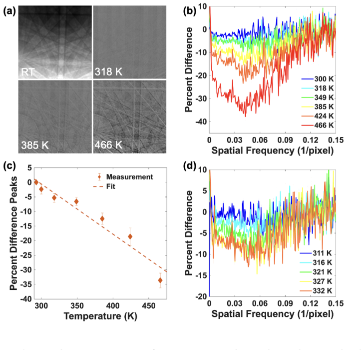
The load-bearing object is the radially integrated magnitude of the two-dimensional spatial Fourier transform of the normalized full EBSD pattern. Temperature acts through the Debye-Waller factor, which suppresses coherent Kikuchi intensity and raises the diffuse background as atomic displacements grow; the Fourier channel near the spatial frequency of the band edges, around 0.04 to 0.06 pixel$^{-1}$, responds almost linearly to temperature. The second essential piece is the direct electron detector, whose low noise and high angular resolution let the experiment resolve these small pattern changes in a 10-second acquisition rather than the minute-scale exposures needed earlier.
What would settle it
Hold a silicon sample at fixed temperature while applying a known uniaxial stress and record the radially integrated Fourier amplitude in the 0.03 to 0.05 pixel$^{-1}$ band; if the amplitude shifts by more than the noise equivalent of about 13 K, the temperature calibration is not strain-independent and gradient maps will need a stress correction.
Extended reading notes
Core claim
The central claim is that thermal diffuse scattering, not thermal expansion, dominates the temperature dependence of EBSD patterns, and that its effect is best read as a global smearing of Kikuchi features rather than as the intensity change of a single band. The paper argues that rising temperature transfers intensity from coherent Kikuchi bands into the diffuse background, blurring band edges in the normalized pattern. A two-dimensional spatial Fourier transform followed by radial integration exposes this blurring as a reproducible change concentrated near a spatial frequency of roughly 0.04 to 0.06 pixel$^{-1}$; the peak change scales linearly with temperature at about 0.15% per K in simulation and 0.14% per K experimentally in silicon. With a 10-second acquisition, the experiment resolves temperature increments of 5 K and reaches a 13-K uncertainty, and the same protocol maps a temperature gradient on a silicon chip, though measured values overestimate the local temperature near strong gradients because thermal stress also alters the pattern.
Load-bearing premise
The readout assumes that the pattern smearing captured by the chosen Fourier component is caused almost entirely by temperature, with strain, surface condition, sample drift, detector drift, and beam-induced damage making negligible or correctable contributions.
Editorial extensions
If this is right
- The full-pattern Fourier readout improves temperature sensitivity by roughly an order of magnitude over single-band intensity analysis (about 0.14% per K versus 0.018% per K).
- A 13-K temperature uncertainty at 10 seconds per point makes multi-point thermal maps of device structures practical in an SEM, where the earlier TDS-based TEM approach required about 96 seconds per point for a 5-K uncertainty.
- Among the four simulated semiconductors, germanium shows the highest temperature coefficient and gallium nitride the lowest, giving a materials ranking for where the technique will work best.
- The same normalized-pattern contrast is robust against fluctuations in overall beam intensity, since normalization removes the dominant experimental nonidealities.
- Spatial temperature mapping under thermal gradients is demonstrated, but measured values overshoot near strong gradients because thermal stress perturbs EBSD patterns; separating that stress contribution is the remaining obstacle.
Reading between the lines
- If strain couples into the same Fourier channel as temperature, the 0.14% per K calibration will not transfer directly to strained device regions; a controlled bending experiment at fixed temperature could quantify that cross-sensitivity.
- The Fourier-amplitude change could be used as a fast screening signal for automated thermal mapping, with machine-learning regression on full patterns as a natural next step to separate TDS from stress and surface artifacts.
- The simulation ranking suggests that materials with stronger Debye-Waller temperature dependence, such as germanium, may reach sub-10-K uncertainty at the same acquisition time; that is a testable prediction, not a demonstrated result.
- Lowering the primary beam energy would shrink the information volume and could improve both spatial resolution and temperature sensitivity simultaneously, provided direct detectors optimized for low-energy electrons become available; the paper identifies this as a direction rather than demonstrating it.
Signed reviews
Editorial analysis
A structured set of objections, weighed in public.
Referee Report
Summary. The manuscript proposes a nanothermometry method based on temperature-induced changes in electron backscattering diffraction (EBSD) patterns acquired with a direct electron detector in an SEM. The authors use dynamical electron simulations (EMSoft) with temperature-dependent Debye-Waller factors and lattice constants to establish theoretical sensitivity for Si, Ge, GaAs, and GaN, and propose a radial Fourier analysis of the full normalized diffraction pattern to quantify the thermal diffuse scattering (TDS) smearing of Kikuchi bands. For silicon they report a simulated sensitivity of 0.149% per K and an experimental sensitivity of 0.14% per K, a 13-K temperature uncertainty at 10 s acquisition time, and distinguishability of 5-K temperature steps. They also attempt spatial temperature mapping across a thermal gradient, but the measured temperatures overestimate the COMSOL-simulated local temperatures, which they attribute to thermal stress affecting EBSD patterns. The central claim is that this is a fast, non-contact, nanometer-resolution thermometry pathway for device-level thermal diagnostics.
Significance. If the sensitivity and speed claims hold, this is a meaningful advance over prior single-band EBSD thermometry (Wu and Hull reported 0.018%/K) and offers an SEM-compatible alternative to TEM-based TDS thermometry, with the practical advantage of minimal sample preparation. The quantitative agreement between simulation (0.149%/K) and experiment (0.14%/K) is a notable strength, as is the use of a direct electron detector with a separate Pt RTD calibration rather than relying on the EBSD signal itself for temperature grounding. The 5-K step resolution and the full-pattern Fourier analysis are genuine contributions. However, the uncertainty metric and the gradient-mapping result, both discussed below, currently limit the strength of the conclusions that can be drawn from the presented evidence.
major comments (3)
- [Section III B, Fig. 6b] The abstract claims that the method can 'enable spatial temperature mapping under thermal gradients,' but the gradient experiment shows that the measured temperatures systematically overestimate the local temperature from the finite-element simulation, particularly near the heater. The authors attribute this to thermal stress affecting EBSD patterns (citing Refs. [39,40]). Because real device hot spots are typically accompanied by thermal stress, the calibration established on a uniform, effectively unstrained sample (0.14%/K) may not transfer to strained device regions. This is a load-bearing issue for the intended application. Please either demonstrate that the Fourier channel used for thermometry is insensitive to stress, provide a calibration that separates strain and temperature contributions, or temper the abstract's claim to reflect that spatial mapping under gradients remains a challenge requiring further calibration.
- [Section III B, Fig. 5c and text after Fig. 5d] The reported 13-K temperature uncertainty is computed as the standard deviation of the Fourier transform magnitude within the spatial frequency range 0.03–0.05 pixel^-1 in a single pattern. This measures scatter across spatial frequencies, not run-to-run or systematic uncertainty. It likely understates the true measurement uncertainty, which would include drift, beam damage, pattern-to-pattern variability, and calibration errors. Since the 13-K number is a central quantitative claim, please report the uncertainty from repeated independent measurements (e.g., multiple acquisitions at the same temperature) or explicitly justify why the within-pattern spectral scatter is an appropriate proxy.
- [Section III A, Fig. 2b/c and Section III B, Fig. 5b/c] The 'most sensitive' Fourier spatial frequency is selected post hoc from the same dataset used to derive the sensitivity: the simulation picks a peak near 0.06 pixel^-1 (Fig. 2c) and the experiment picks a peak near 0.04 pixel^-1 (Fig. 5c). Because the analysis channel is not predefined, the reported 0.149%/K and 0.14%/K are optimized values, and the simulation/experiment comparison is not testing the same observable. This selection bias could overstate the sensitivity of a fixed protocol. Please pre-specify the analysis channel or report the sensitivity averaged over a wider, fixed frequency band, and discuss the discrepancy between the simulated and experimental optimal frequencies.
minor comments (3)
- [Throughout] There are several typographical errors: 'indispensible' (Introduction), 'acquitision' (Introduction, paragraph on TEM TDS), 'requisition time' (Introduction, paragraph on secondary electron emission), 'GaAa' (Section II.A), 'eletron beam heating' (Section II.B), and 'Navel' (Acknowledgments, should be 'Naval').
- [Section III A, Fig. 2c and Section III B, Fig. 5c] The simulated optimal frequency is stated as about 0.06 pixel^-1 while the experimental one is about 0.04 pixel^-1. Please clarify whether this difference arises from detector geometry, pattern size, or simulation parameters, and whether the quoted sensitivity values are directly comparable.
- [Section II.B] The sentence 'There was a minimum of 5 minutes between changes in voltage and capture of EBSD patterns' should be rephrased for clarity, e.g., 'At least 5 minutes elapsed between changing the voltage and capturing the EBSD pattern, to allow temperature stabilization.'
Circularity Check
No circularity: the calibration path is independent and the main limitations are transferability concerns, not definitional loops.
full rationale
The paper's derivation chain is self-contained against external benchmarks. In simulation, the temperature-dependent EBSD patterns are produced by EMSoft using lattice constants from literature and Debye-Waller factors from an externally published DFT parametrization (Schowalter et al.); no temperature-sensitivity output is fed back into the simulation inputs. In experiment, the EBSD Fourier signal is calibrated against a separately fabricated Pt RTD whose resistance is measured independently of the EBSD pattern, and the reported 0.14%/K slope is a measured calibration, not a fitted parameter renamed as a prediction. The spatial temperature map then applies that calibration to a new location; the authors themselves report that the map overestimates local temperature under a large gradient and attribute this to thermal stress affecting EBSD patterns, which is an honest validity/transferability caveat rather than a circular step. The post-hoc selection of the most sensitive Fourier channel and the use of the standard deviation of Fourier amplitude as the 13-K uncertainty are methodological selection/error-estimation issues, not instances where a prediction reduces to its input by construction. The self-citations [37,38] describe detector installation and performance and are not load-bearing for the central thermometry claim. No equation in the paper equates its output to its input by definition, and no load-bearing uniqueness theorem or ansatz is imported solely from the authors' prior work. Therefore the circularity score is 0.
Assumptions & free parameters
free parameters (3)
- Fourier radial-frequency channel (thermometry readout) =
0.06 pixel^-1 in simulation; 0.03 to 0.05 pixel^-1 averaging band in experiment
- Experimentally fitted temperature coefficient =
0.14%/K
- Debye-Waller B(T) coefficients =
From DFT parametrization in Schowalter et al. [36]
assumptions (6)
- domain assumption Bloch-wave dynamical diffraction combined with Monte Carlo backscattering, as implemented in EMSoft, accurately reproduces EBSD pattern intensities including TDS.
- domain assumption The temperature-dependent Debye-Waller factors from Schowalter et al. correctly describe TDS for Si, Ge, GaAs, and GaN.
- domain assumption Normalization by average pattern intensity removes all non-temperature intensity fluctuations.
- domain assumption Thermal expansion contributes negligibly to the measured signal compared with TDS.
- domain assumption Electron-beam-induced heating of the sample is below 0.1 K.
- domain assumption The backscattered-electron escape diameter of roughly 40 nm defines the thermal measurement region.
Cite this review
Pith. "Pith review of Fast nanothermometry based on direct electron detection of electron backscattering diffraction patterns." pith.science (2026). https://pith.science/paper/BYIWYKT3
@misc{pith2026250705467,
  author       = {Pith},
  title        = {Pith review of: Fast nanothermometry based on direct electron detection of electron backscattering diffraction patterns},
  year         = {2026},
  howpublished = {\url{https://pith.science/paper/BYIWYKT3}},
  note         = {Machine review of arXiv:2507.05467}
}
read the original abstract
Accurate temperature measurement at the nanoscale is crucial for thermal management in next-generation microelectronic devices. Existing optical and scanning-probe thermometry techniques face limitations in spatial resolution, accuracy, or invasiveness. In this work, we demonstrate a fast and non-contact nanothermometry method based on temperature-induced changes in electron backscattering diffraction (EBSD) patterns captured by a high-performance direct electron detector within a scanning electron microscope (SEM). Using dynamical electron simulations, we establish the theoretical temperature sensitivity limits for several semiconductors (Si, Ge, GaAs, and GaN), showing that thermal diffuse scattering (TDS) leads to a measurable smearing of Kikuchi bands in the EBSD patterns. We develop a Fourier analysis method that captures these subtle changes across the full diffraction pattern, achieving a simulated temperature sensitivity of approximately 0.15\% per K. Experimental results on silicon confirm a sensitivity of 0.14\% per K and achieve a 13-K temperature uncertainty with a 10-second acquisition time, and enable spatial temperature mapping under thermal gradients. Our approach offers a pathway toward practical and high-resolution thermal mapping directly in SEMs, expanding the toolbox for device-level thermal diagnostics.
Figures


Figures from the paper (3 more)


Reference graph
Works this paper leans on
-
[1]
Y. Qin, B. Albano, J. Spencer, J. S. Lundh, B. Wang, C. Buttay, M. Tadjer, C. DiMarino, and Y. Zhang, Thermal management and packaging of wide and ultra-wide bandgap power devices: a review and perspective, Journal of physics D: applied physics 56, 093001 (2023)
work page 2023
-
[2]
Z. Li, H. Luo, Y. Jiang, H. Liu, L. Xu, K. Cao, H. Wu, P. Gao, and H. Liu, Comprehensive review and future prospects on chip-scale thermal management: Core of data center’s thermal management, Applied Thermal Engineering , 123612 (2024)
work page 2024
-
[3]
S. Choi, S. Graham, S. Chowdhury, E. R. Heller, M. J. Tadjer, G. Moreno, and S. Narumanchi, A perspective on the electro-thermal co-design of ultra-wide bandgap lateral devices, Applied Physics Letters 119 (2021)
work page 2021
-
[4]
J. Schleeh, J. Mateos, I. ´I˜ niguez-de-la Torre, N. Wadefalk, P.-A. Nilsson, J. Grahn, and A. Min- nich, Phonon black-body radiation limit for heat dissipation in electronics, Nature Materials 14, 187 (2015). 17
work page 2015
-
[5]
M. Malakoutian, K. Woo, D. Rich, R. Mandia, X. Zheng, A. Kasperovich, D. Saraswat, R. Soman, Y. Jo, T. Pfeifer, et al., Lossless phonon transition through GaN-diamond and Si-diamond interfaces, Advanced Electronic Materials 11, 2400146 (2025)
work page 2025
-
[6]
C. Mion, J. Muth, E. Preble, and D. Hanser, Accurate dependence of gallium nitride thermal conductivity on dislocation density, Applied Physics Letters 89 (2006)
work page 2006
- [7]
-
[8]
A. J. Schmidt, R. Cheaito, and M. Chiesa, A frequency-domain thermoreflectance method for the characterization of thermal properties, Review of Scientific Instruments 80 (2009)
work page 2009
Show all 40 references
-
[9]
Choudhry, T
U. Choudhry, T. Kim, M. Adams, J. Ranasinghe, R. Yang, and B. Liao, Characterizing mi- croscale energy transport in materials with transient grating spectroscopy, Journal of Applied Physics 130 (2021)
2021
-
[10]
Beechem, A
T. Beechem, A. Christensen, S. Graham, and D. Green, Micro-raman thermometry in the presence of complex stresses in GaN devices, Journal of Applied Physics 103 (2008)
2008
-
[11]
Sokalski, Z
P. Sokalski, Z. Han, G. C. Fleming, B. Smith, S. E. Sullivan, R. Huang, X. Ruan, and L. Shi, Effects of hot phonons and thermal stress in micro-raman spectra of molybdenum disulfide, Applied Physics Letters 121 (2022)
2022
-
[12]
K. R. Bagnall, E. A. Moore, S. C. Badescu, L. Zhang, and E. N. Wang, Simultaneous measure- ment of temperature, stress, and electric field in GaN HEMTs with micro-Raman spectroscopy, Review of Scientific Instruments 88 (2017)
2017
-
[13]
Z. Ye, B. Harrington, and A. D. Pickel, Optical super-resolution nanothermometry via stimulated emission depletion imaging of upconverting nanoparticles, Science Advances 10, eado6268 (2024)
2024
-
[14]
Zhang, W
Y. Zhang, W. Zhu, F. Hui, M. Lanza, T. Borca-Tasciuc, and M. Mu˜ noz Rojo, A review on principles and applications of scanning thermal microscopy (SThM), Advanced Functional Materials 30, 1900892 (2020)
2020
-
[15]
Reihani, Z
A. Reihani, Z. Li, J. Guan, Y. Luan, S. Yan, J. Xue, E. Meyhofer, P. Reddy, and R. J. Ram, Cooling of semiconductor devices via quantum tunneling, Physical Review Letters 133, 266301 (2024). 18
2024
-
[16]
Menges, H
F. Menges, H. Riel, A. Stemmer, and B. Gotsmann, Nanoscale thermometry by scanning thermal microscopy, Review of Scientific Instruments 87 (2016)
2016
-
[17]
K. E. Goodson and M. Asheghi, Near-field optical thermometry, Microscale Thermophysical Engineering 1, 225 (1997)
1997
-
[18]
Ezugwu, S
S. Ezugwu, S. Kazemian, D.-Y. W. Choi, and G. Fanchini, Contactless near-field scanning thermoreflectance imaging, Nanoscale 9, 4097 (2017)
2017
-
[19]
Z. L. Wang, Thermal diffuse scattering in sub-angstrom quantitative electron mi- croscopy—phenomenon, effects and approaches, Micron 34, 141 (2003)
2003
-
[20]
Wehmeyer, K
G. Wehmeyer, K. C. Bustillo, A. M. Minor, and C. Dames, Measuring temperature-dependent thermal diffuse scattering using scanning transmission electron microscopy, Applied Physics Letters 113 (2018)
2018
-
[21]
Niekiel, S
F. Niekiel, S. M. Kraschewski, J. M¨ uller, B. Butz, and E. Spiecker, Local temperature mea- surement in tem by parallel beam electron diffraction, Ultramicroscopy 176, 161 (2017)
2017
-
[22]
Mecklenburg, W
M. Mecklenburg, W. A. Hubbard, E. White, R. Dhall, S. B. Cronin, S. Aloni, and B. Regan, Nanoscale temperature mapping in operating microelectronic devices, Science 347, 629 (2015)
2015
-
[23]
J. C. Idrobo, A. R. Lupini, T. Feng, R. R. Unocic, F. S. Walden, D. S. Gardiner, T. C. Lovejoy, N. Dellby, S. T. Pantelides, and O. L. Krivanek, Temperature measurement by a nanoscale electron probe using energy gain and loss spectroscopy, Physical Review Letters 120, 095901 (2018)
2018
-
[24]
M. Khan, S. Lubner, D. Ogletree, and C. Dames, Temperature dependence of secondary electron emission: A new route to nanoscale temperature measurement using scanning electron microscopy, Journal of Applied Physics 124 (2018)
2018
-
[25]
Wu and R
X. Wu and R. Hull, A novel nano-scale non-contact temperature measurement technique for crystalline materials, Nanotechnology 23, 465707 (2012)
2012
-
[26]
Wu and R
X. Wu and R. Hull, The material dependence of temperature measurement resolution in thermal scanning electron microscopy, Applied Physics Letters 102 (2013)
2013
-
[27]
Zaefferer, On the formation mechanisms, spatial resolution and intensity of backscatter Kikuchi patterns, Ultramicroscopy 107, 254 (2007)
S. Zaefferer, On the formation mechanisms, spatial resolution and intensity of backscatter Kikuchi patterns, Ultramicroscopy 107, 254 (2007)
2007
-
[28]
Humphreys, Review grain and subgrain characterisation by electron backscatter diffraction, Journal of Materials Science 36, 3833 (2001)
F. Humphreys, Review grain and subgrain characterisation by electron backscatter diffraction, Journal of Materials Science 36, 3833 (2001). 19
2001
-
[29]
Ouyang, X
W. Ouyang, X. Zuo, and B. Liao, Impact of photoexcitation on secondary electron emission: A Monte Carlo study, Journal of Applied Physics 133 (2023)
2023
-
[30]
P. G. Callahan and M. De Graef, Dynamical electron backscatter diffraction patterns. Part I: Pattern simulations, Microscopy and Microanalysis 19, 1255 (2013)
2013
-
[31]
Singh, F
S. Singh, F. Ram, and M. De Graef, EMsoft: open source software for electron diffrac- tion/image simulations, Microscopy and Microanalysis 23, 212 (2017)
2017
-
[32]
Okada and Y
Y. Okada and Y. Tokumaru, Precise determination of lattice parameter and thermal expansion coefficient of silicon between 300 and 1500 K, Journal of Applied Physics 56, 314 (1984)
1984
-
[33]
R. R. Reeber and K. Wang, Thermal expansion and lattice parameters of group IV semicon- ductors, Materials Chemistry and Physics 46, 259 (1996)
1996
-
[34]
Vurgaftman, J
I. Vurgaftman, J. Meyer, and L. R. Ram-Mohan, Band parameters for III–V compound semi- conductors and their alloys, Journal of Applied Physics 89, 5815 (2001)
2001
-
[35]
Roder, S
C. Roder, S. Einfeldt, S. Figge, and D. Hommel, Temperature dependence of the thermal expansion of GaN, Physical Review B 72, 085218 (2005)
2005
-
[36]
Schowalter, A
M. Schowalter, A. Rosenauer, J. Titantah, and D. Lamoen, Computation and parametriza- tion of the temperature dependence of Debye–Waller factors for group IV, III–V and II–VI semiconductors, Foundations of Crystallography 65, 5 (2009)
2009
-
[37]
F. Wang, M. P. Echlin, A. A. Taylor, J. Shin, B. Bammes, B. D. Levin, M. De Graef, T. M. Pollock, and D. S. Gianola, Electron backscattered diffraction using a new monolithic direct detector: High resolution and fast acquisition, Ultramicroscopy 220, 113160 (2021)
2021
-
[38]
N. M. Della Ventura, A. R. Ericks, M. P. Echlin, K. Moore, T. M. Pollock, M. R. Begley, F. W. Zok, M. De Graef, and D. S. Gianola, Direct electron detection for EBSD of low symmetry & beam sensitive ceramics, Ultramicroscopy 268, 114079 (2025)
2025
-
[39]
S. I. Wright, M. M. Nowell, and D. P. Field, A review of strain analysis using electron backscat- ter diffraction, Microscopy and microanalysis 17, 316 (2011)
2011
-
[40]
Wang, J.-C
F. Wang, J.-C. Stinville, M. Charpagne, M. P. Echlin, S. R. Agnew, T. M. Pollock, M. De Graef, and D. S. Gianola, Dislocation cells in additively manufactured metallic alloys characterized by electron backscatter diffraction pattern sharpness, Materials Characterization 197, 1...
2023
Reviewed August 6, 2026 · model on record in the stance chip above.
Discussion (0). Continue with ORCID to comment.