High yield creation of germanium vacancy centers in diamond by focused ion beam implantation and high temperature annealing
Pith reviewed 2026-06-30 01:02 UTC · model grok-4.3
The pith
Focused ion beam implantation creates GeV centers in diamond with yields up to 33%.
A machine-rendered reading of the paper's core claim, the machinery that carries it, and where it could break.
Core claim
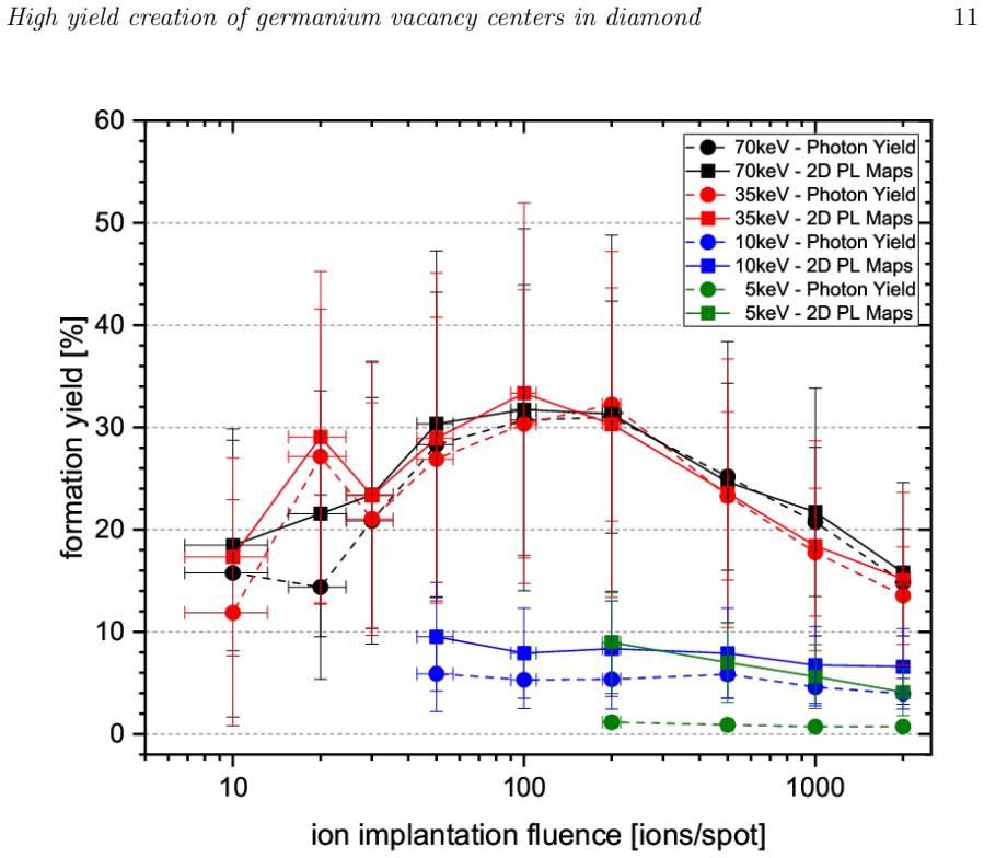
Negatively charged germanium vacancy centers form in diamond when germanium ions are delivered by focused ion beam implantation at energies of 35 and 70 keV and low fluences, followed by high-temperature annealing; the process achieves a maximum formation yield of 33% and places centers across depths of 5.5 to 30 nm.
What carries the argument
Focused ion beam implantation at selected energies and fluences followed by high-temperature annealing, which controls depth and produces GeV centers at high yield in a localized volume.
If this is right
- Low-fluence implantation produces isolated single GeV centers.
- Centers appear only inside a small, well-defined local volume.
- Yield peaks at 33% for implantation energies of 35 keV and 70 keV.
- The method supplies a route to embed GeV centers inside nanophotonic structures.
Where Pith is reading between the lines
- The localized nature of the beam may limit lattice damage outside the target region compared with broad-beam methods.
- The same process parameters could be tested on other vacancy centers to check whether high yields are general.
- Depth control between 5.5 nm and 30 nm may allow alignment of centers with specific optical mode profiles in fabricated devices.
Load-bearing premise
The defects produced are negatively charged GeV centers that possess the optical properties needed for quantum applications.
What would settle it
Observation of the characteristic zero-phonon line emission from the created centers together with direct confirmation of the negative charge state.
Figures
read the original abstract
Negatively charged germanium vacancy centers (GeV) in diamond are a promising platform for quantum computing and quantum communication. However, these applications require the precise incorporation of GeV centers with good optical properties inside of nanophotonic structures. In this work, we demonstrate the highly efficient local creation of GeV centers in diamond via focused-ion-beam implantation, followed by high-temperature annealing. We report the successful creation of GeV centers over the depth range of 5.5 - 30 nm. Implantation at low fluence enables the creation of single GeV centers. The formation yield strongly depends on implantation energy and fluence, reaching up to 33% at energies of 35 and 70 keV. This method, therefore, enables the efficient creation of GeV centers within a small, well-defined local sample volume and offers a potential means of incorporating them into photonic structures.
Editorial analysis
A structured set of objections, weighed in public.
Referee Report
Summary. The manuscript reports an experimental demonstration of creating negatively charged germanium-vacancy (GeV) centers in diamond by focused-ion-beam implantation of Ge ions at 35 keV and 70 keV followed by high-temperature annealing. GeV centers are formed over depths 5.5–30 nm; yields reach 33 % at the cited energies, single centers are obtained at low fluence, and the approach is proposed for incorporation into nanophotonic structures.
Significance. If the reported yields, depth control, and single-center creation are reproducible, the work supplies a practical, localized fabrication route for a promising quantum defect. The quantified dependence of yield on implantation energy and fluence supplies actionable parameters for device integration; the experimental workflow (implantation parameters plus annealing protocol) is a concrete contribution to the field.
major comments (2)
- [Results (yield measurements)] Results section on yield versus fluence: the central 33 % yield figure is load-bearing for the efficiency claim, yet the text supplies neither the total number of implanted ions, the counted center statistics, nor error bars; without these the quoted percentage cannot be evaluated for statistical significance.
- [Characterization] Characterization subsection: confirmation that the observed centers are negatively charged GeV (rather than other color centers) rests on optical spectra and charge-state identification; the manuscript must show representative zero-phonon-line spectra, linewidth data, or charge-state switching measurements to support the claim that the centers possess the optical properties required for quantum applications.
minor comments (2)
- [Methods] Methods: the annealing temperature, duration, and ambient conditions are stated but the ramp rates and cooling protocol are omitted; these details affect reproducibility.
- [Figure captions] Figure captions: depth values (5.5–30 nm) should be cross-referenced to the SRIM or experimental depth-profile data used to establish the range.
Simulated Author's Rebuttal
We thank the referee for the positive evaluation and the detailed comments that will improve the manuscript. We address each major comment below.
read point-by-point responses
-
Referee: Results section on yield versus fluence: the central 33 % yield figure is load-bearing for the efficiency claim, yet the text supplies neither the total number of implanted ions, the counted center statistics, nor error bars; without these the quoted percentage cannot be evaluated for statistical significance.
Authors: We agree that these details are essential. The revised manuscript now includes the total number of implanted ions (derived from the fluence and implanted area), the number of counted GeV centers from the optical measurements, and error bars for the yield values. This information is added to the Results section to enable assessment of statistical significance. revision: yes
-
Referee: Characterization subsection: confirmation that the observed centers are negatively charged GeV (rather than other color centers) rests on optical spectra and charge-state identification; the manuscript must show representative zero-phonon-line spectra, linewidth data, or charge-state switching measurements to support the claim that the centers possess the optical properties required for quantum applications.
Authors: We appreciate this suggestion. In the revised version, we have included representative zero-phonon-line spectra, measured linewidths, and data on charge-state switching to rigorously confirm the identification as negatively charged GeV centers and their suitability for quantum applications. revision: yes
Circularity Check
No significant circularity
full rationale
This is a purely experimental report with no equations, fitted models, derivations, or load-bearing self-citations. The central claims rest on implantation parameters, annealing protocols, depth measurements, and direct counting statistics for GeV center creation and yield; none of these reduce by construction to the paper's own inputs or prior self-citations. The workflow is self-contained against external benchmarks such as measured fluences, energies, and observed defect counts.
Axiom & Free-Parameter Ledger
axioms (1)
- domain assumption Diamond lattice remains intact enough after FIB implantation and annealing to host stable, optically active GeV centers
Reference graph
Works this paper leans on
-
[1]
Material platforms for defect qubits and single- photon emitters,
G. Zhang, Y. Cheng, J.-P. Chou, and A. Gali, “Material platforms for defect qubits and single- photon emitters,”Applied Physics Reviews, vol. 7, no. 3, 2020
2020
-
[2]
Quantum technologies with optically interfaced solid-state spins,
D. D. Awschalom, R. Hanson, J. Wrachtrup, and B. B. Zhou, “Quantum technologies with optically interfaced solid-state spins,”Nature Photonics, vol. 12, no. 9, pp. 516–527, 2018
2018
-
[3]
Quantum nanophotonics with group iv defects in diamond,
C. Bradac, W. Gao, J. Forneris, M. E. Trusheim, and I. Aharonovich, “Quantum nanophotonics with group iv defects in diamond,”Nature communications, vol. 10, no. 1, p. 5625, 2019
2019
-
[4]
Ultralong spin coherence time in isotopically engineered diamond,
G. Balasubramanian, P. Neumann, D. Twitchen, M. Markham, R. Kolesov, N. Mizuochi, J. Isoya, J. Achard, J. Beck, J. Tissler, V. Jacques, P. R. Hemmer, F. Jelezko, and J. Wrachtrup, “Ultralong spin coherence time in isotopically engineered diamond,”Nature Materials, vol. 8, may 2009
2009
-
[5]
The nitrogen-vacancy colour centre in diamond,
M. W. Doherty, N. B. Manson, P. Delaney, F. Jelezko, J. Wrachtrup, and L. C. Hollenberg, “The nitrogen-vacancy colour centre in diamond,”Physics Reports, vol. 528, no. 1, pp. 1–45, 2013. The nitrogen-vacancy colour centre in diamond
2013
-
[6]
Magnetometry with nitrogen-vacancy defects in diamond,
L. Rondin, J.-P. Tetienne, T. Hingant, J.-F. Roch, P. Maletinsky, and V. Jacques, “Magnetometry with nitrogen-vacancy defects in diamond,”Reports on Progress in Physics, vol. 77, p. 056503, may 2014
2014
-
[7]
High-precision nanoscale temperature sensing using single defects in diamond,
P. Neumann, I. Jakobi, F. Dolde, C. Burk, R. Reuter, G. Waldherr, J. Honert, T. Wolf, A. Brunner, J. H. Shim, D. Suter, H. Sumiya, J. Isoya, and J. Wrachtrup, “High-precision nanoscale temperature sensing using single defects in diamond,”Nano Letters, vol. 13, jun 2013
2013
-
[8]
Nanometre-scale thermometry in a living cell,
G. Kucsko, P. C. Maurer, N. Y. Yao, M. Kubo, H. J. Noh, P. K. Lo, H. Park, and M. D. Lukin, “Nanometre-scale thermometry in a living cell,”Nature, vol. 500, aug 2013
2013
-
[9]
Properties of nitrogen-vacancy centers in diamond: the group theoretic approach,
J. R. Maze, A. Gali, E. Togan, Y. Chu, A. Trifonov, E. Kaxiras, and M. D. Lukin, “Properties of nitrogen-vacancy centers in diamond: the group theoretic approach,”New Journal of Physics, vol. 13, p. 025025, feb 2011
2011
-
[10]
Impact of surface and laser- induced noise on the spectral stability of implanted nitrogen-vacancy centers in diamond,
S. Chakravarthi, C. Pederson, Z. Kazi, A. Ivanov, and K.-M. C. Fu, “Impact of surface and laser- induced noise on the spectral stability of implanted nitrogen-vacancy centers in diamond,”Phys. Rev. B, vol. 104, p. 085425, Aug 2021
2021
-
[11]
Probing coherence properties of shallow implanted nv ensembles under different oxygen terminations,
J. Fuhrmann, J. Lang, J. Scharpf, N. Striegler, T. Unden, P. Neumann, J. Bansmann, and F. Jelezko, “Probing coherence properties of shallow implanted nv ensembles under different oxygen terminations,”Materials for Quantum Technology, vol. 4, p. 041001, dec 2024
2024
-
[12]
Single photon emission from silicon-vacancy colour centres in chemical vapour deposition nano- diamonds on iridium,
E. Neu, D. Steinmetz, J. Riedrich-M¨ oller, S. Gsell, M. Fischer, M. Schreck, and C. Becher, “Single photon emission from silicon-vacancy colour centres in chemical vapour deposition nano- diamonds on iridium,”New Journal of Physics, vol. 13, p. 025012, feb 2011
2011
-
[13]
Germanium-vacancy single color centers in diamond,
T. Iwasaki, F. Ishibashi, Y. Miyamoto, Y. Doi, S. Kobayashi, T. Miyazaki, K. Tahara, K. D. Jahnke, L. J. Rogers, B. Naydenov, F. Jelezko, S. Yamasaki, S. Nagamachi, T. Inubushi, N. Mizuochi, and M. Hatano, “Germanium-vacancy single color centers in diamond,”Sci. Rep., vol. 5, p. 12882, Aug. 2015
2015
-
[14]
Tin-vacancy quantum emitters in diamond,
T. Iwasaki, Y. Miyamoto, T. Taniguchi, P. Siyushev, M. H. Metsch, F. Jelezko, and M. Hatano, “Tin-vacancy quantum emitters in diamond,”Phys. Rev. Lett., vol. 119, p. 253601, Dec 2017
2017
-
[15]
Single-photon emitters in lead-implanted single- crystal diamond,
S. Ditalia Tchernij, T. L¨ uhmann, T. Herzig, J. K¨ upper, A. Damin, S. Santonocito, M. Signorile, P. Traina, E. Moreva, F. Celegato, S. Pezzagna, I. P. Degiovanni, P. Olivero, M. Jakˇ si´ c, High yield creation of germanium vacancy centers in diamond16 J. Meijer, P. M. Genovese, and J. Forneris, “Single-photon emitters in lead-implanted single- crystal d...
2018
-
[16]
Silicon-vacancy spin qubit in diamond: A quantum memory exceeding 10 ms with single-shot state readout,
D. D. Sukachev, A. Sipahigil, C. T. Nguyen, M. K. Bhaskar, R. E. Evans, F. Jelezko, and M. D. Lukin, “Silicon-vacancy spin qubit in diamond: A quantum memory exceeding 10 ms with single-shot state readout,”Phys. Rev. Lett., vol. 119, p. 223602, Nov 2017
2017
-
[17]
Microwave control of the tin-vacancy spin qubit in diamond with a superconducting waveguide,
I. Karapatzakis, J. Resch, M. Schrodin, P. Fuchs, M. Kieschnick, J. Heupel, L. Kussi, C. S¨ urgers, C. Popov, J. Meijer, C. Becher, W. Wernsdorfer, and D. Hunger, “Microwave control of the tin-vacancy spin qubit in diamond with a superconducting waveguide,”Phys. Rev. X, vol. 14, p. 031036, Aug 2024
2024
-
[18]
Initialization and readout of nuclear spins via a negatively charged silicon-vacancy center in diamond,
M. H. Metsch, K. Senkalla, B. Tratzmiller, J. Scheuer, M. Kern, J. Achard, A. Tallaire, M. B. Plenio, P. Siyushev, and F. Jelezko, “Initialization and readout of nuclear spins via a negatively charged silicon-vacancy center in diamond,”Phys. Rev. Lett., vol. 122, p. 190503, May 2019
2019
-
[19]
High-fidelity control of a 13C nuclear spin coupled to a tin-vacancy center in diamond,
J. Resch, I. Karapatzakis, M. Elshorbagy, M. Schrodin, P. Fuchs, P. Graßhoff, L. Kussi, C. S¨ urgers, C. Popov, C. Becher, W. Wernsdorfer, and D. Hunger, “High-fidelity control of a 13C nuclear spin coupled to a tin-vacancy center in diamond,”Phys. Rev. X, vol. 16, p. 011060, Mar 2026
2026
-
[20]
Germanium vacancy in diamond quantum memory exceeding 20 ms,
K. Senkalla, G. Genov, M. H. Metsch, P. Siyushev, and F. Jelezko, “Germanium vacancy in diamond quantum memory exceeding 20 ms,”Phys. Rev. Lett., vol. 132, p. 026901, Jan 2024
2024
-
[21]
Coherent control of a long-lived nuclear memory spin in a germanium-vacancy multi-qubit node,
N. Grimm, K. Senkalla, P. J. Vetter, J. Frey, P. Gundlapalli, T. Calarco, G. Genov, M. M. M¨ uller, and F. Jelezko, “Coherent control of a long-lived nuclear memory spin in a germanium-vacancy multi-qubit node,”Phys. Rev. Lett., vol. 134, p. 043603, Jan 2025
2025
-
[22]
Formation yield of germanium- vacancy centers in diamond upon kev ion nano-implantation and thermal annealing,
V. Pugliese, G. Gavello, E. N. Hernandez, E. Redolfi, E. Scattolo, A. Cian, E. Missale, A. Bortone, R. Dell’Anna, S. D. Tchernij, D. Giubertoni, and J. Forneris, “Formation yield of germanium- vacancy centers in diamond upon kev ion nano-implantation and thermal annealing,”J. Appl. Phys., vol. 138, July 2025
2025
-
[23]
Integration of germanium-vacancy single photon emitters arrays in diamond nanopillars,
E. Redolfi, V. Pugliese, E. Scattolo, A. Cian, E. Missale, F. Favaro de Oliveira, G. Seniutinas, S. Ditalia Tchernij, R. Dell’Anna, P. Traina, P. Olivero, D. Giubertoni, and J. Forneris, “Integration of germanium-vacancy single photon emitters arrays in diamond nanopillars,”EPJ Quantum Technol., vol. 12, Dec. 2025
2025
-
[24]
Quantum nonlinear optics with a germanium-vacancy color center in a nanoscale diamond waveguide,
M. K. Bhaskar, D. D. Sukachev, A. Sipahigil, R. E. Evans, M. J. Burek, C. T. Nguyen, L. J. Rogers, P. Siyushev, M. H. Metsch, H. Park, F. Jelezko, M. Lonˇ car, and M. D. Lukin, “Quantum nonlinear optics with a germanium-vacancy color center in a nanoscale diamond waveguide,” Phys. Rev. Lett., vol. 118, May 2017
2017
-
[25]
Direct writing of single germanium vacancy center arrays in diamond,
Y. Zhou, Z. Mu, G. Adamo, S. Bauerdick, A. Rudzinski, I. Aharonovich, and W. bo Gao, “Direct writing of single germanium vacancy center arrays in diamond,”New Journal of Physics, vol. 20, p. 125004, dec 2018
2018
-
[26]
Large-scale integration of artificial atoms in hybrid photonic circuits,
N. H. Wan, T.-J. Lu, K. C. Chen, M. P. Walsh, M. E. Trusheim, L. De Santis, E. A. Bersin, I. B. Harris, S. L. Mouradian, I. R. Christen, E. S. Bielejec, and D. Englund, “Large-scale integration of artificial atoms in hybrid photonic circuits,”Nature, vol. 583, pp. 226–231, July 2020
2020
-
[27]
Quantum interference of resonance fluorescence from germanium- vacancy color centers in diamond,
D. Chen, J. E. Fr¨ och, S. Ru, H. Cai, N. Wang, G. Adamo, J. Scott, F. Li, N. Zheludev, I. Aharonovich, and W. Gao, “Quantum interference of resonance fluorescence from germanium- vacancy color centers in diamond,”Nano Lett., vol. 22, pp. 6306–6312, Aug. 2022
2022
-
[28]
Efficiency optimization of Ge-V quantum emitters in single-crystal diamond upon ion implantation and HPHT annealing,
E. Nieto Hern´ andez, E. Redolfi, C. Stella, G. Andrini, E. Corte, S. Sachero, S. Ditalia Tchernij, F. Picariello, T. Herzig, Y. M. Borzdov, I. N. Kupriyanov, A. Kubanek, P. Olivero, J. Meijer, P. Traina, Y. N. Palyanov, and J. Forneris, “Efficiency optimization of Ge-V quantum emitters in single-crystal diamond upon ion implantation and HPHT annealing,”A...
2023
-
[29]
Bright single-photon emission from a GeV center in diamond under a microfabricated solid immersion lens at room temperature,
J. Christinck, F. Hirt, H. Hofer, Z. Liu, M. Etzkorn, T. Dunatov, M. Jakˇ si´ c, J. Forneris, and S. K¨ uck, “Bright single-photon emission from a GeV center in diamond under a microfabricated solid immersion lens at room temperature,”J. Appl. Phys., vol. 133, May 2023
2023
-
[30]
Cavity-enhanced High yield creation of germanium vacancy centers in diamond17 photon emission from a single germanium-vacancy center in a diamond membrane,
R. Høy Jensen, E. Janitz, Y. Fontana, Y. He, O. Gobron, I. P. Radko, M. Bhaskar, R. Evans, C. D. Rodr´ ıguez Rosenblueth, L. Childress, A. Huck, and U. Lund Andersen, “Cavity-enhanced High yield creation of germanium vacancy centers in diamond17 photon emission from a single germanium-vacancy center in a diamond membrane,”Phys. Rev. Appl., vol. 13, June 2020
2020
-
[31]
Structural formation yield of GeV centers from implanted Ge in diamond,
U. Wahl, J. G. Correia, A. Costa, A. Lamelas, V. Amaral, K. Johnston, G. Magchiels, S. M. Tunhuma, A. Vantomme, and L. M. C. Pereira, “Structural formation yield of GeV centers from implanted Ge in diamond,”Materials for Quantum Technology, vol. 4, p. 025101, May 2024
2024
-
[32]
Lifetime reduction of single germanium-vacancy centers in diamond via a tunable open microcavity,
R. Zifkin, C. D. Rodr´ ıguez Rosenblueth, E. Janitz, Y. Fontana, and L. Childress, “Lifetime reduction of single germanium-vacancy centers in diamond via a tunable open microcavity,” PRX quantum, vol. 5, July 2024
2024
-
[33]
Creation of colour centres in diamond by collimated ion- implantation through nano-channels in mica,
S. Pezzagna, D. Rogalla, H.-W. Becker, I. Jakobi, F. Dolde, B. Naydenov, J. Wrachtrup, F. Jelezko, C. Trautmann, and J. Meijer, “Creation of colour centres in diamond by collimated ion- implantation through nano-channels in mica,”Phys. Status Solidi (A), vol. 208, pp. 2017–2022, Sept. 2011
2017
-
[34]
Highly tunable formation of nitrogen- vacancy centers via ion implantation,
S. Sangtawesin, T. Brundage, Z. Atkins, and J. R. Petta, “Highly tunable formation of nitrogen- vacancy centers via ion implantation,”Applied Physics Letters, vol. 105, no. 6, 2014
2014
-
[35]
Maskless and targeted creation of arrays of colour centres in diamond using focused ion beam technology,
M. Lesik, P. Spinicelli, S. Pezzagna, P. Happel, V. Jacques, O. Salord, B. Rasser, A. Delobbe, P. Sudraud, A. Tallaire,et al., “Maskless and targeted creation of arrays of colour centres in diamond using focused ion beam technology,”physica status solidi (a), vol. 210, no. 10, pp. 2055– 2059, 2013
2055
-
[36]
Array of bright silicon-vacancy centers in diamond fabricated by low-energy focused ion beam implantation,
S. Tamura, G. Koike, A. Komatsubara, T. Teraji, S. Onoda, L. P. McGuinness, L. Rogers, B. Naydenov, E. Wu, L. Yan,et al., “Array of bright silicon-vacancy centers in diamond fabricated by low-energy focused ion beam implantation,”Applied Physics Express, vol. 7, no. 11, p. 115201, 2014
2014
-
[37]
Scalable focused ion beam creation of nearly lifetime- limited single quantum emitters in diamond nanostructures,
T. Schr¨ oder, M. E. Trusheim, M. Walsh, L. Li, J. Zheng, M. Schukraft, A. Sipahigil, R. E. Evans, D. D. Sukachev, C. T. Nguyen,et al., “Scalable focused ion beam creation of nearly lifetime- limited single quantum emitters in diamond nanostructures,”Nature communications, vol. 8, no. 1, p. 15376, 2017
2017
-
[38]
Fabrication of conductive graphitic layers in diamond by multispecies focused ion beam,
E. Scattolo, E. Missale, A. Cian, M. Valt, S. Ferrari, G. Speranza, R. Dell’Anna, and D. Giubertoni, “Fabrication of conductive graphitic layers in diamond by multispecies focused ion beam,” physica status solidi (a), vol. 223, no. 7, p. e202500645, 2026
2026
-
[39]
Extending spin coherence times of diamond qubits by high-temperature annealing,
T. Yamamoto, T. Umeda, K. Watanabe, S. Onoda, M. L. Markham, D. J. Twitchen, B. Naydenov, L. P. McGuinness, T. Teraji, S. Koizumi, F. Dolde, H. Fedder, J. Honert, J. Wrachtrup, T. Ohshima, F. Jelezko, and J. Isoya, “Extending spin coherence times of diamond qubits by high-temperature annealing,”Physical Review B, vol. 88, p. 075206, Aug. 2013
2013
-
[40]
Multispecies focused ion beam lithography system and its applications,
S. Bauerdick, L. Bruchhaus, P. Mazarov, A. Nadzeyka, R. Jede, J. Fridmann, J. E. Sanabia, B. Gila, and B. R. Appleton, “Multispecies focused ion beam lithography system and its applications,” Journal of Vacuum Science & Technology B, vol. 31, no. 6, 2013
2013
-
[41]
Liquid metal alloy ion sources—an alternative for focussed ion beam technology,
L. Bischoff, P. Mazarov, L. Bruchhaus, and J. Gierak, “Liquid metal alloy ion sources—an alternative for focussed ion beam technology,”Applied Physics Reviews, vol. 3, no. 2, 2016
2016
-
[42]
Srim–the stopping and range of ions in matter (2010),
J. F. Ziegler, M. D. Ziegler, and J. P. Biersack, “Srim–the stopping and range of ions in matter (2010),”Nuclear Instruments and Methods in Physics Research Section B: Beam Interactions with Materials and Atoms, vol. 268, no. 11-12, pp. 1818–1823, 2010
2010
-
[43]
Long optical coherence times of shallow-implanted, negatively charged silicon vacancy centers in diamond,
J. Lang, S. H¨ außler, J. Fuhrmann, R. Waltrich, S. Laddha, J. Scharpf, A. Kubanek, B. Naydenov, and F. Jelezko, “Long optical coherence times of shallow-implanted, negatively charged silicon vacancy centers in diamond,”Applied Physics Letters, vol. 116, p. 064001, 02 2020
2020
-
[44]
Qudi: A modular python suite for experiment control and data processing,
J. M. Binder, A. Stark, N. Tomek, J. Scheuer, F. Frank, K. D. Jahnke, C. M¨ uller, S. Schmitt, M. H. Metsch, T. Unden, T. Gehring, A. Huck, U. L. Andersen, L. J. Rogers, and F. Jelezko, “Qudi: A modular python suite for experiment control and data processing,”SoftwareX, vol. 6, pp. 85–90, Jan. 2017
2017
-
[45]
Array of bright silicon-vacancy centers in diamond fabricated by low-energy focused ion beam implantation,
S. Tamura, G. Koike, A. Komatsubara, T. Teraji, S. Onoda, L. P. McGuinness, L. Rogers, B. Naydenov, E. Wu, L. Yan, F. Jelezko, T. Ohshima, J. Isoya, T. Shinada, and T. Tanii, High yield creation of germanium vacancy centers in diamond18 “Array of bright silicon-vacancy centers in diamond fabricated by low-energy focused ion beam implantation,”Applied Phys...
2014
-
[46]
Generation of single color centers by focused nitrogen implantation,
J. Meijer, B. Burchard, M. Domhan, C. Wittmann, T. Gaebel, I. Popa, F. Jelezko, and J. Wrachtrup, “Generation of single color centers by focused nitrogen implantation,”Applied Physics Letters, vol. 87, p. 261909, 12 2005
2005
-
[47]
Creation of silicon- vacancy color centers in diamond by ion implantation,
S. Lagomarsino, A. M. Flatae, H. Kambalathmana, F. Sledz, L. Hunold, N. Soltani, P. Reuschel, S. Sciortino, N. Gelli, M. Massi, C. Czelusniak, L. Giuntini, and M. Agio, “Creation of silicon- vacancy color centers in diamond by ion implantation,”Frontiers in Physics, vol. Volume 8 - 2020, 2021
2020
-
[48]
Creation efficiency of nitrogen- vacancy centres in diamond,
S. Pezzagna, B. Naydenov, F. Jelezko, J. Wrachtrup, and J. Meijer, “Creation efficiency of nitrogen- vacancy centres in diamond,”New Journal of Physics, vol. 12, p. 065017, jun 2010
2010
-
[49]
Damage threshold for ion-beam induced graphitization of diamond,
C. Uzan-Saguy, C. Cytermann, R. Brener, V. Richter, M. Shaanan, and R. Kalish, “Damage threshold for ion-beam induced graphitization of diamond,”Applied Physics Letters, vol. 67, pp. 1194–1196, 08 1995
1995
-
[50]
Integration of germanium-vacancy single photon emitters arrays in diamond nanopillars,
E. Redolfi, V. Pugliese, E. Scattolo, A. Cian, E. Missale, F. Favaro de Oliveira, G. Seniutinas, S. Ditalia Tchernij, R. Dell’Anna, P. Traina, P. Olivero, D. Giubertoni, and J. Forneris, “Integration of germanium-vacancy single photon emitters arrays in diamond nanopillars,”EPJ Quantum Technology, vol. 12, pp. 1–15, Dec. 2025
2025
discussion (0)
Sign in with ORCID, Apple, or X to comment. Anyone can read and Pith papers without signing in.