REVIEW 3 major objections 4 minor 55 references
Design triple points, nexus points and related topological phases by stacking monolayers
T0 review · 3 major / 4 minor · reviewed 2026-08-14 · deepseek-v4-flash
Pith's one-line read Stacking one insulator and one metal monolayer creates triple points and tangle nodal lines in a 3D crystal.
desk verdict A clean, testable design rule for triple/nexus points from stacked monolayers; the DFT materials case is plausible but leaves the strain question unexamined. read the letter →
The pith
A machine-rendered reading of the paper's core claim, the machinery that carries it, and where it could break.
The reading
What carries the argument
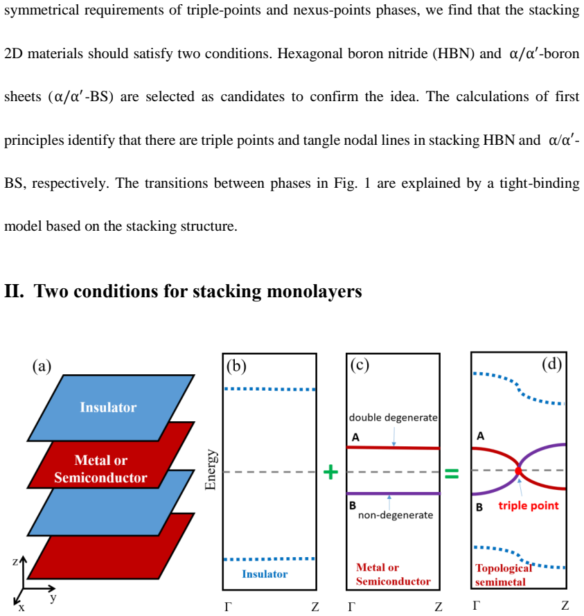
The central object is the stacking geometry of two C3-symmetric monolayers and the interlayer hopping it activates. In the isolated layers the relevant bands are flat along the stacking direction; interlayer coupling gives them dispersion along $k_z$, so the doubly degenerate band from the metal and the nondegenerate band from the insulator can cross. The presence or absence of a mirror plane parallel to the layers decides whether the crossing is a triple point or a nexus point: with the mirror plane, a trivial quadratic nodal line connects two triple points; without it, that line splits into four linear topological nodal lines. The tight-binding Hamiltonian of Eq. (1), with one $p_z$ orbital per atom, captures this because only $p_z$ states contribute near the Fermi level.
What would settle it
Compute the band structure of the HBN/α′-BS stack with the in-plane lattice constant relaxed to the equilibrium α′-BS value of 5.21 Å and look at the Γ point along Γ–Z: if the doubly degenerate and nondegenerate bands no longer cross, the predicted tangle nodal-line phase is absent. Equivalently, a search of the first Brillouin zone at the strained lattice constant should find the four nodal lines of Fig. 5(b); failing to find them would refute the claim.
Extended reading notes
Core claim
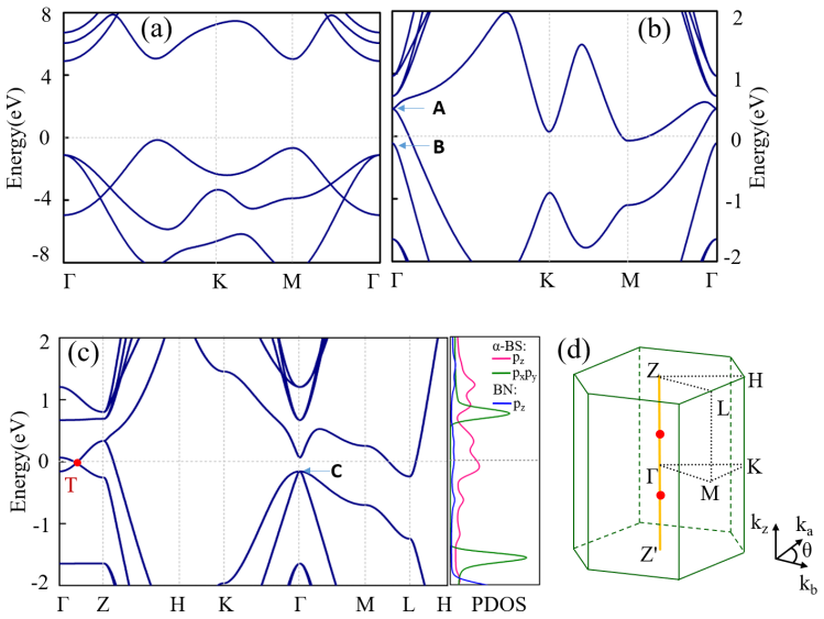
The central claim is that interlayer interactions in an alternating stack of a C3-symmetric insulator and a C3-symmetric metal/semiconductor turn the flat bands of the isolated layers into a three-band crossing (triple point) or, when the parallel mirror plane is absent, into four topological nodal lines that merge at nexus points and can evolve into tangle nodal lines. Concretely, the authors find by first-principles calculation that HBN/α-BS stacking produces two triple points at $k_z = \pm 0.21\pi/c$ linked by a quadratic nodal line along Γ–Z, while HBN/α′-BS stacking, in which α′-BS lacks the horizontal mirror plane, produces a tangle of four nodal lines in the first Brillouin zone. The mechanism does not require the insulator to conduct or the metal to be particularly special; it only requires the two monolayer band features at Γ and the shared rotation/mirror symmetries.
Load-bearing premise
The calculations force the boron sheets to sit at a strained in-plane lattice constant (2.53 Å, about 3% mismatch) and do not check whether the required doubly degenerate and nondegenerate bands at Γ survive that strain; if strain lifts the degeneracy, the triple points and tangle nodal lines would not form as described.
Editorial extensions
If this is right
- Any pair of monolayers satisfying the two conditions should, when stacked alternately, show triple points or nexus points rather than requiring a bespoke 3D crystal.
- In the specific HBN/α-BS stack, the two triple points are linked by a trivial quadratic nodal line along Γ–Z, so the phase is the one shown in Fig. 1(a).
- Removing the parallel mirror plane—here by switching from flat α-BS to buckled α′-BS—turns the triple-point phase into tangle nodal lines, matching the transition in Fig. 1(g).
- The one-orbital tight-binding model reproduces all four phases (triple points, nexus points, critical phase, tangle nodal lines) by tuning interlayer hoppings, so the mechanism is not an artefact of one material pair.
- Other symmetry-preserving stacking designs could yield nodal chains, Hopf links, or nodal surfaces.
Reading between the lines
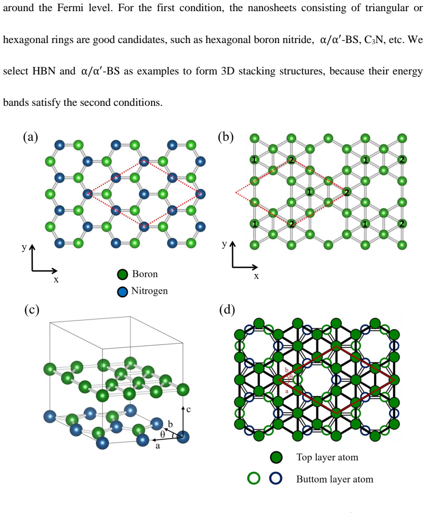
- Because the DFT calculations force a 2×2 HBN cell (5.06 Å) to match the α/α′-BS primitive cell at 2.53 Å, the ~3% strain on the boron sheets is absorbed without comment; a natural check is whether the Γ-point degeneracy and the crossings survive at the equilibrium boron lattice constant.
- The same two conditions could be screened across existing monolayer databases to predict new van der Waals superlattices with triple or nexus points, without additional symmetry analysis.
- If interlayer hopping can be tuned continuously (e.g., by pressure or twist angle), the tight-binding map from triple points to nexus points to tangle nodal lines suggests the phase can be switched in a single device.
- The paper's tangle-nodal-line phase in HBN/α′-BS would be falsifiable by angle-resolved photoemission, since the nodal lines sit in the $k_z = 0$ and mirror planes and should produce characteristic surface arcs.
Signed reviews
Editorial analysis
A structured set of objections, weighed in public.
Referee Report
Summary. The paper proposes a general design principle for realizing three-dimensional topological phases—triple points, nexus points, and related nodal-line phases—by alternately stacking two types of two-dimensional monolayers. The authors state two conditions for the constituent monolayers: (i) the monolayers must have a C3 rotation axis and three mirror planes along that axis, and (ii) one monolayer must be insulating while the other is metallic or semiconducting with a doubly degenerate band and a non-degenerate band at the Γ point near the Fermi level. They identify hexagonal boron nitride (HBN) and α/α′-boron sheets as candidate materials. Using first-principles DFT, they report triple points in stacked HBN/α-BS and a tangle nodal-line phase in stacked HBN/α′-BS. A tight-binding model with hand-tuned parameters is used to illustrate the phase transitions among triple points, nexus points, and tangle nodal lines.
Significance. If the central claim holds, the paper offers a simple and physically intuitive recipe for engineering topological phases in three dimensions by stacking two-dimensional building blocks, which could substantially broaden the search space for topological materials. The explicit identification of two candidate stacks and the first-principles band structures are valuable additions. The conceptual framework, linking monolayer symmetries and band topology to stack-induced crossings, is appealing and likely to stimulate further work. However, the manuscript currently leaves important technical questions unresolved—most notably the role of lattice mismatch and strain—and the topological characterization of the reported phases is incomplete. These issues must be resolved before the design principle can be considered firmly established.
major comments (3)
- [Section III] The reported lattice constants are internally inconsistent. The text states that the primitive lattice constants of α/α′-BS are a0 = b0 = 5.21 Å and those of HBN are a1 = b1 = 2.53 Å, and that a 2×2 HBN supercell (5.06 Å) matches the α/α′-BS primitive cell to within 3%. Yet it then states that the optimized lattice constants of the 3D stacking structures are a2 = b2 = 2.53 Å. A commensurate 3D cell should have an in-plane lattice constant near 5.06–5.21 Å, not 2.53 Å. The authors must clarify the actual computational cell used in the DFT calculations and reconcile this apparent contradiction, since the reported band structures depend critically on the assumed in-plane periodicity.
- [Section III] Even if the computational cell is the expected 2×2 HBN supercell, the α/α′-BS layer is subjected to roughly 3% compressive strain relative to its equilibrium lattice constant. The paper does not examine whether this strain preserves the doubly degenerate band and non-degenerate band at Γ that are required by the second condition. The band structures in Figs. 4(c) and 5(a) are computed at the strained in-plane lattice constant, but the authors do not report the strained monolayer band structure, the variation of the band ordering with strain, or the total energy as a function of in-plane lattice constant. Without such an analysis, it is unclear whether the reported triple points and nodal lines are robust features of the proposed design or accidental consequences of an unrealistically strained geometry.
- [Section III] The identification of the triple point at kz = 0.21π/c in Fig. 4(c) is based only on the band structure along Γ–Z. The paper does not verify the topological charge of this crossing, nor does it present the full three-dimensional dispersion in the kx–ky plane to confirm that the crossing is a genuine triple point of the type shown in Fig. 1(a). Similarly, for the tangle nodal lines in Fig. 5(b), the evidence is a crossing on a single mirror plane, and the connectivity of the four nodal lines is not demonstrated. The authors should compute the band structure in a plane perpendicular to Γ–Z around the triple point and trace the nodal-line connectivity in three dimensions to substantiate the claimed topological phases.
minor comments (4)
- [Throughout] There are several typographical errors and inconsistent notations: “strcture” in the caption of Fig. 4(d), “α − BSare” in Section III, and “α/α′-SB” versus “α/α′-BS” used interchangeably. Please proofread the manuscript carefully.
- [Section III] In Fig. 4(b), the points labeled A and B are mentioned in the text but not defined in the caption. Please add a brief explanation of these labels in the figure caption.
- [Section IV] The tight-binding model parameters in Table 1 are not derived from the DFT calculations; the values are chosen to reproduce the different phases. The authors should state more clearly that the TB model is illustrative and not quantitatively fitted to the first-principles results, so that readers do not overinterpret the phase-transition sequences.
- [Section IV and Table 1] The notation t7, t'7, t8, t'8 is introduced in the text but not explicitly defined in Eqs. (2)–(4) or in Fig. 6. Please ensure that all hopping parameters appearing in Table 1 are defined and labeled consistently with the figures.
Circularity Check
No significant circularity: the central proposal is grounded in independent DFT calculations, and the tight-binding model is explicitly parameter-tuned rather than presented as a parameter-free prediction.
full rationale
The paper's central claim is that alternating stacks of monolayers satisfying two stated conditions—C3 symmetry with three mirror planes, and one insulating plus one metallic/semiconducting monolayer with a doubly degenerate and a non-degenerate band at Γ—can realize triple points, nexus points, and related phases. This claim is tested by first-principles DFT (VASP, PBE) for HBN/α-BS and HBN/α′-BS stacks, which independently show triple points and tangle nodal lines respectively. The monolayer band-structure conditions are inputs to the search, not outputs derived from the target phases, and the 3D calculations go beyond the monolayer inputs by including interlayer coupling. The tight-binding model in Section IV is explicitly tuned: 'By tuning the parameters in Eqs. (2-4), one can get all the phases in Fig. 1,' with parameters listed in Table 1. It is therefore a fitted demonstration or explanation of the phase transitions, not a prediction claimed to be independent of those fits, so it does not constitute circularity in the derivation of the central result. The self-citations in the reference list (e.g., refs. 24, 27, 43) are contextual and not load-bearing; the symmetry conditions are supported by non-self citations (refs. 25, 33). The possible strain issue—the 3D stack is computed at a2=b2=2.53 Å while free-standing α/α′-BS has a0=5.21 Å, with the paper noting a mismatch below 3%—is a robustness or correctness concern, not a circularity: the DFT result is still a genuine calculation, and the paper does not redefine the target phases in terms of the calculated bands.
Assumptions & free parameters
free parameters (2)
- Site energies eps1, eps2, eps3 in tight-binding model =
-1.4, -3.5, -3.0 eV
- Hopping parameters t_alpha, t_beta, t_gamma (including inequivalent t7/t'7, t8/t'8) =
Listed in Table 1 (values not reproduced in the text provided)
assumptions (3)
- domain assumption Symmetry requirements (C3 rotation and three vertical mirror planes) protect triple points, nexus points, and the associated nodal lines.
- domain assumption Interlayer coupling bends the flat monolayer bands to produce crossings, while preserving the monolayer band character and symmetry.
- domain assumption PBE functional with Grimme-D3 describes the electronic structure and interlayer interactions well enough for the predicted phases.
Cite this review
Pith. "Pith review of Design triple points, nexus points and related topological phases by stacking monolayers." pith.science (2026). https://pith.science/paper/C4RRGM7Z
@misc{pith2026190809467,
  author       = {Pith},
  title        = {Pith review of: Design triple points, nexus points and related topological phases by stacking monolayers},
  year         = {2026},
  howpublished = {\url{https://pith.science/paper/C4RRGM7Z}},
  note         = {Machine review of arXiv:1908.09467}
}
read the original abstract
Triple points and nexus points are two interesting topological phases, which have been reported in some three-dimensional (3D) materials. Here, we propose that triple points, nexus points and related phases, such as topological tangle nodal lines, can be obtained by alternatively stacking two types of monolayers. Two conditions for the stacking monolayers are required: the first condition is that they have a three-fold (C3) rotation symmetry and three mirror planes along the C3 axis; the second condition is that one of the monolayers should be insulating while the other one should be metallic (or semiconducting) and has a double degenerate band and a nondegenerate band at {\Gamma}point around the Fermi level. Hexagonal boron nitride (HBN) and {\alpha}/{\alpha}^'-boron sheets ({\alpha}/{\alpha}^'-BS) are suggested as candidate materials. Even if HBN is a wide-gap insulator, the interactions between layers lead to crossings of the nondegenerate and double degenerate bands along the direction normal to the nanosheets, and thus form triple/nexus points or related phases. A tight-binding model is adopted to explain the phase transition between triple points, nexus points and other related phases.
Figures

Figures from the paper (2 more)

Reference graph
Works this paper leans on
-
[1]
M. Z. Hasan and C. L. Kane, Rev. Mod. Phys. 82, 3045 (2010)
2010
-
[2]
L. Fu, C. L. Kane, and E. J. Mele, Phys. Rev. Lett. 98, 106803 (2007)
2007
- [3]
-
[4]
Huang, S
H. Huang, S. Zhou, and W. Duan, Phys. Rev. B 94, 121117 (2016)
2016
-
[5]
L. Lu, Z. Wang, D. Ye, L. Ran, L. Fu, J. D. Joannopoulos, and M. Soljačić, Science 349, 622 (2015)
2015
-
[6]
T. Bzdušek, Q. Wu, A. Rüegg, M. Sigrist, and A. A. Soluyanov, Nature 538, 75 (2016)
work page 2016
-
[7]
Z. Wang, Y. Sun, X.-Q. Chen, C. Franchini, G. Xu, H. Weng, X. Dai, and Z. Fang, Phys. Rev. B 85, 195320 (2012)
work page 2012
- [8]
Show all 55 references
-
[9]
Liu et al., Nat
Z. Liu et al., Nat. Mater. 13, 677 (2014)
2014
-
[10]
Y. Chen, Y. Xie, S. A. Yang, H. Pan, F. Zhang, M. L. Cohen, and S. Zhang, Nano Lett. 15, 6974 (2015)
2015
-
[11]
H. Weng, C. Fang, Z. Fang, B. A. Bernevig, and X. Dai, Phys. Rev. X 5, 011029 (2015)
2015
-
[12]
Zhong, Y
C. Zhong, Y. Chen, Z.-M. Yu, Y. Xie, H. Wang, S. A. Yang, and S. Zhang, Nat. Commun. 8, 15641 (2017)
2017
-
[13]
C. Fang, Y. Chen, H.-Y. Kee, and L. Fu, Phys. Rev. B 92, 081201 (2015)
2015
-
[14]
Huang, J
H. Huang, J. Liu, D. Vanderbilt, and W. Duan, Phys. Rev. B 93, 201114 (2016)
2016
-
[15]
Y. Kim, B. J. Wieder, C. Kane, and A. M. Rappe, Phys. Rev. Lett. 115, 036806 (2015)
2015
-
[16]
Chang et al., Phys
G. Chang et al., Phys. Rev. Lett. 119, 156401 (2017)
2017
-
[17]
R. Yu, H. Weng, Z. Fang, X. Dai, and X. Hu, Phys. Rev. Lett. 115, 036807 (2015)
2015
-
[18]
J.-T. Wang, H. Weng, S. Nie, Z. Fang, Y. Kawazoe, and C. Chen, Phys. Rev. Lett. 116, 195501 (2016)
2016
-
[19]
W. Wu, Y. Liu, S. Li, C. Zhong, Z.-M. Yu, X.-L. Sheng, Y. Zhao, and S. A. Yang, Phys. Rev. B 97, 115125 (2018)
2018
-
[20]
Zhong, Y
C. Zhong, Y. Chen, Y. Xie, S. A. Yang, M. L. Cohen, and S. Zhang, Nanoscale 8, 7232 (2016)
2016
-
[21]
Zhang, Z.-M
X. Zhang, Z.-M. Yu, Z. Zhu, W. Wu, S.-S. Wang, X.-L. Sheng, and S. A. Yang, Phys. Rev. B 97, 235150 (2018)
2018
-
[22]
Fulga, L
I. Fulga, L. Fallani, and M. Burrello, Phys. Rev. B 97, 121402 (2018)
2018
-
[23]
Z.-G. Song, C. Felser, and Y. Sun, Phys. Rev. B 98, 165131 (2018)
2018
-
[24]
Y. Xie, J. Cai, J. Kim, P.-Y. Chang, and Y. Chen, Phys. Rev. B 99, 165147 (2019)
2019
-
[25]
Z. Zhu, G. W. Winkler, Q. Wu, J. Li, and A. A. Soluyanov, Phys. Rev. X 6, 031003 (2016)
2016
-
[26]
Guo, H.-C
P.-J. Guo, H.-C. Yang, K. Liu, and Z.-Y. Lu, Phys. Rev. B 98, 045134 (2018)
2018
-
[27]
J. Cai, Y. Xie, P.-Y. Chang, H.-S. Kim, and Y.-P. Chen, Phys. Chem. Chem. Phys. (2018)
2018
-
[28]
J.-P. Sun, D. Zhang, and K. Chang, Phys. Rev. B 96, 045121 (2017)
2017
-
[29]
Zhang, Z.-M
T.-T. Zhang, Z.-M. Yu, W. Guo, D. Shi, G. Zhang, and Y. Yao, J. Phys. Chem. Lett. 8, 5792 (2017)
2017
-
[30]
H. Weng, C. Fang, Z. Fang, and X. Dai, Phys. Rev. B 94, 165201 (2016). 16
2016
-
[31]
H. Yang, J. Yu, S. S. Parkin, C. Felser, C.-X. Liu, and B. Yan, Phys. Rev. Lett. 119, 136401 (2017)
2017
-
[32]
L. Jin, X. Zhang, X. Dai, H. Liu, G. Chen, and G. Liu, J. Mater. Chem. C 7, 1316 (2019)
2019
-
[33]
Chang et al., Sci
G. Chang et al., Sci. Rep. 7, 1688 (2017)
2017
-
[34]
H. Weng, C. Fang, Z. Fang, and X. Dai, Phys. Rev. B 93, 241202 (2016)
2016
-
[35]
Hyart and T
T. Hyart and T. Heikkilä , Phys. Rev. B 93, 235147 (2016)
2016
-
[36]
Jin, Y.-J
H.-S. Jin, Y.-J. Song, W. E. Pickett, and K.-W. Lee, Phys. Rev. Mater. 3, 021201 (2019)
2019
-
[37]
Mikitik and Y
G. Mikitik and Y. V. Sharlai, Phys. Rev. B 73, 235112 (2006)
2006
-
[38]
T. T. Heikkilä and G. E. Volovik, New J. Phys. 17, 093019 (2015)
2015
-
[39]
Vergniory, L
M. Vergniory, L. Elcoro, C. Felser, N. Regnault, B. A. Bernevig, and Z. Wang, Nature 566, 480 (2019)
2019
-
[40]
F. Tang, H. C. Po, A. Vishwanath, and X. Wan, Nat. Phys., 1 (2019)
2019
-
[41]
Zhang, Y
T. Zhang, Y. Jiang, Z. Song, H. Huang, Y. He, Z. Fang, H. Weng, and C. Fang, Nature 566, 475 (2019)
2019
-
[42]
F. Tang, H. C. Po, A. Vishwanath, and X. Wan, Nature 566, 486 (2019)
2019
-
[43]
Y. Chen, Y. Xie, Y. Gao, P.-Y. Chang, S. Zhang, and D. Vanderbilt, Phys. Rev. Mater. 2, 044205 (2018)
2018
-
[44]
K.-H. Ahn, W. E. Pickett, and K.-W. Lee, Phys. Rev. B 98, 035130 (2018)
2018
-
[45]
Ma et al., Nat
J.-Z. Ma et al., Nat. Phys. 14, 349 (2018)
2018
-
[46]
A. K. Geim, Science 324, 1530 (2009)
2009
-
[47]
Bafekry, S
A. Bafekry, S. Farjami Shayesteh, and F. M. Peeters, The Journal of Physical Chemistry C (2019)
2019
-
[48]
Sevik, Phys
C. Sevik, Phys. Rev. B 89, 035422 (2014)
2014
-
[49]
Splendiani, L
A. Splendiani, L. Sun, Y. Zhang, T. Li, J. Kim, C.-Y. Chim, G. Galli, and F. Wang, Nano Lett. 10, 1271 (2010)
2010
-
[50]
Y. Shao, M. F. El-Kady, L. J. Wang, Q. Zhang, Y. Li, H. Wang, M. F. Mousavi, and R. B. Kaner, Chem. Soc. Rev. 44, 3639 (2015)
2015
-
[51]
X. Wu, J. Dai, Y. Zhao, Z. Zhuo, J. Yang, and X. C. Zeng, ACS nano 6, 7443 (2012)
2012
-
[52]
J. P. Perdew, K. Burke, and M. Ernzerhof, Phys. Rev. Lett. 77, 3865 (1996)
1996
-
[53]
Kresse and D
G. Kresse and D. Joubert, Phys. Rev. B 59, 1758 (1999)
1999
-
[54]
Kresse and J
G. Kresse and J. Furthmü ller, Phys. Rev. B 54, 11169 (1996)
1996
-
[55]
Schlü ter, J
M. Schlü ter, J. R. Chelikowsky, S. G. Louie, and M. L. Cohen, Phys. Rev. B 12, 4200 (1975)
1975
Reviewed August 14, 2026 · model on record in the stance chip above.
Discussion (0). Continue with ORCID to comment.