Compositional and Magnetic Characterisation of Oblique Co and Fe Nanowire Structures Fabricated Using Focused Electron Beam Induced Deposition
Pith reviewed 2026-06-30 20:32 UTC · model grok-4.3
The pith
Tuning electron beam voltage and current lets FEBID produce Co and Fe nanowires with roughly equal metal content at growth angles up to 60 degrees.
A machine-rendered reading of the paper's core claim, the machinery that carries it, and where it could break.
Core claim
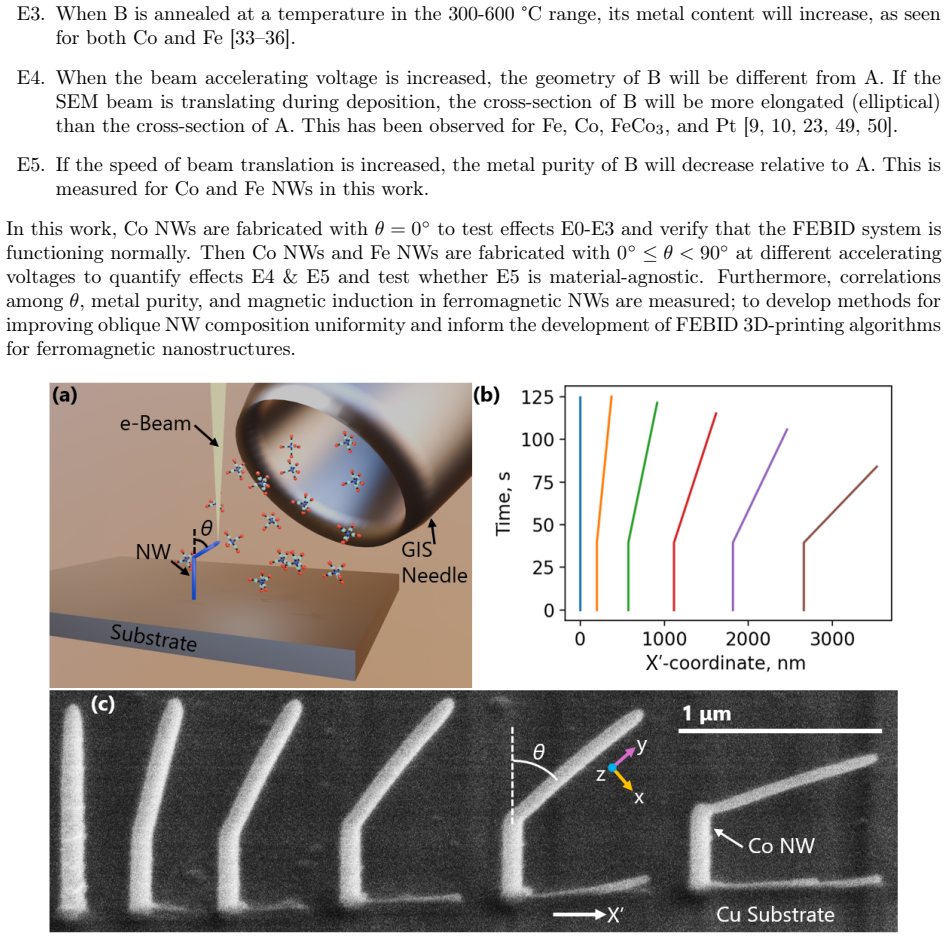
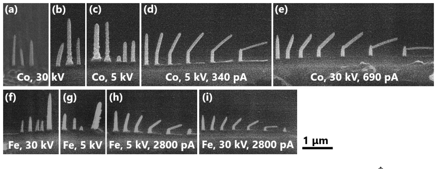
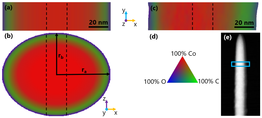
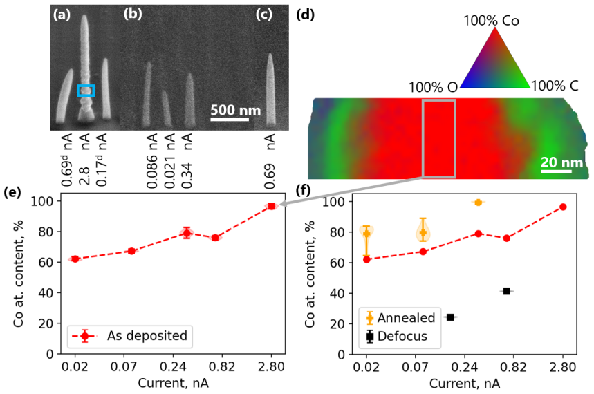
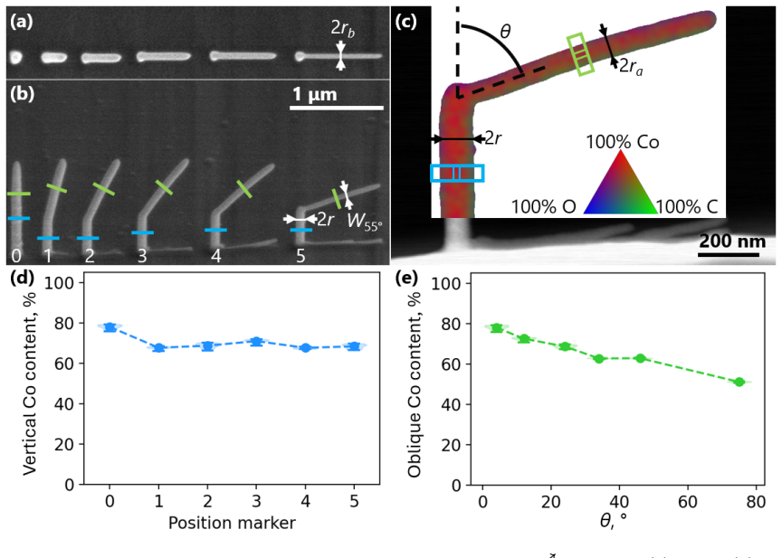
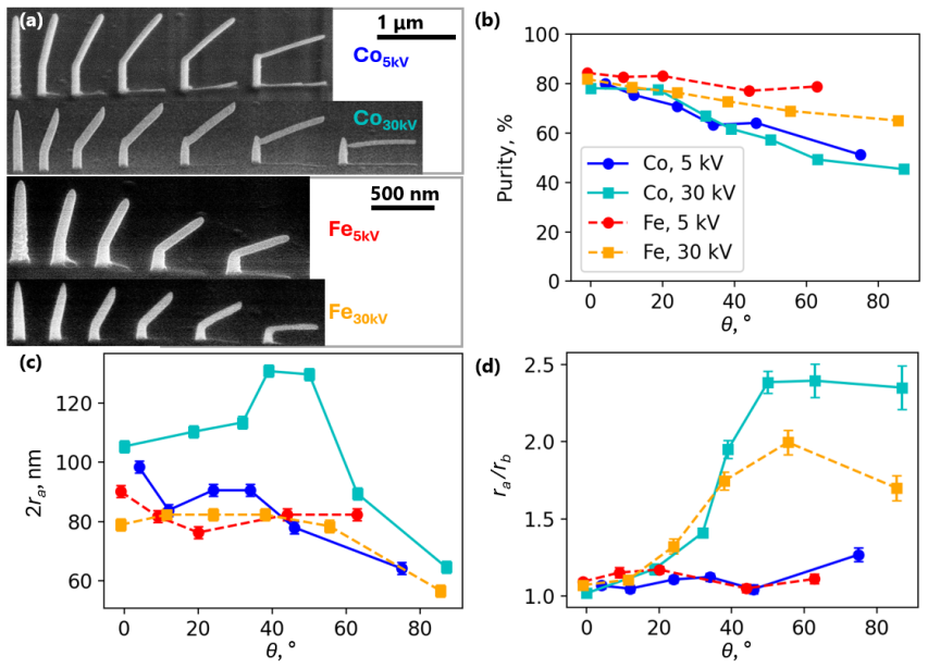
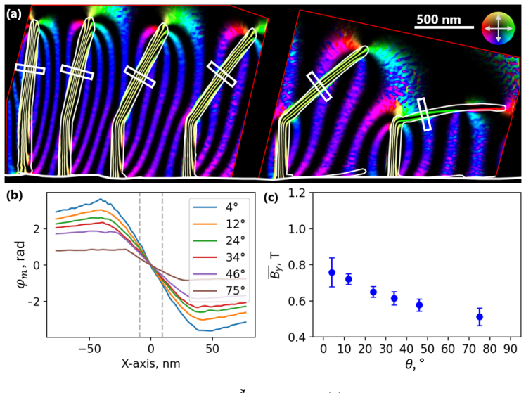
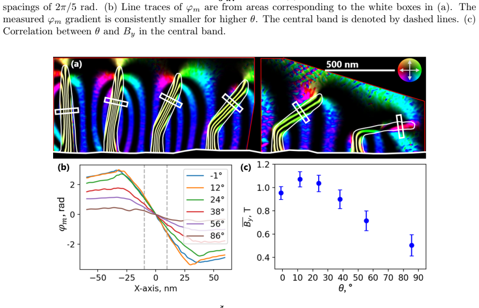
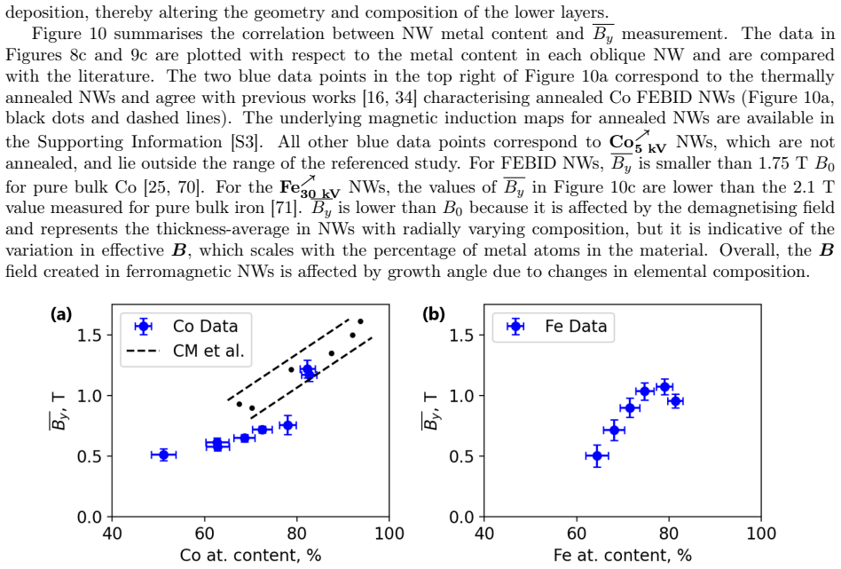
Ferromagnetic NWs with approximately equal metal content at growth angles from 0° to 60° were fabricated by using the lowest viable electron beam voltage and the highest viable beam current to reduce the interaction volume and increase the metal content, respectively. Comparison of the results reveals a reduction in metal content with increased oblique growth angle in FEBID NWs. The magnitude of metal content reduction can be tuned by controlling electron beam parameters.
What carries the argument
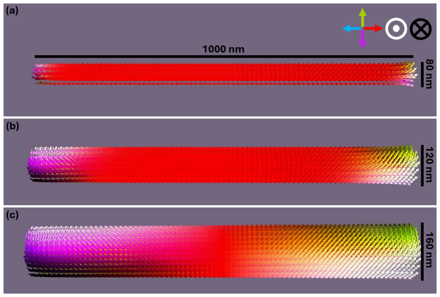
FEBID growth of Co and Fe nanowires at controlled oblique angles, with atomic composition mapped by electron energy loss spectroscopy and magnetic induction mapped by off-axis electron holography.
If this is right
- Metal content in FEBID nanowires decreases as the oblique growth angle increases.
- The size of the metal-content reduction can be controlled by changing electron beam voltage and current.
- Optimized low-voltage, high-current beams produce nanowires with nearly constant metal content from 0° to 60°.
- Magnetic induction varies in step with the measured changes in metal content.
- Structures with overhanging or bridged elements can be grown with more uniform composition.
Where Pith is reading between the lines
- The same beam-parameter choice may allow uniform composition in other FEBID materials beyond Co and Fe.
- Complex 3D spintronic prototypes could be made without later correction steps for composition gradients.
- Further reduction of interaction volume might extend uniform growth beyond 60 degrees.
- Reliability of magnetic devices built from such nanowires could improve if composition is held constant.
Load-bearing premise
The observed drop in metal content is caused primarily by growth angle and interaction volume rather than by other uncontrolled variables in the deposition process or in the microscopy measurements.
What would settle it
Growing nanowires at 60 degrees with the lowest viable voltage and highest viable current and measuring substantially lower metal content than in 0-degree nanowires would show that equal content cannot be maintained.
Figures
read the original abstract
Focused electron beam induced deposition (FEBID) is an additive manufacturing technique uniquely suited for fabricating nanoscale 3D prototypes for a range of applications, including spintronic devices. However, the variation of growth dynamics associated with electron beam translation and sample interaction volumes results in structures with non-uniform composition when fabricating intricate 3D geometries. Herein, we measure changes in atomic composition and corresponding changes in magnetic induction in 3D ferromagnetic nanostructures with overhanging elements, e.g. bridges or arches. To investigate the effects of electron beam translation, we fabricated 41 Co and Fe nanowire (NW) structures with growth angle relative to the optic axis varying from 0{\deg} to 90{\deg}. The (scanning) transmission electron microscopy techniques of electron energy loss spectroscopy and off-axis electron holography were performed to map the NW elemental composition and magnetic induction as a function of NW growth angle. Comparison of the results reveals a reduction in metal content with increased oblique growth angle in FEBID NWs. The magnitude of metal content reduction can be tuned by controlling electron beam parameters, and ferromagnetic NWs with approximately equal metal content at growth angles from 0{\deg} to 60{\deg} were fabricated by using the lowest viable electron beam voltage and the highest viable beam current to reduce the interaction volume and increase the metal content, respectively.
Editorial analysis
A structured set of objections, weighed in public.
Referee Report
Summary. The manuscript reports fabrication of 41 Co and Fe nanowire structures by FEBID with growth angles from 0° to 90° relative to the optic axis. Using EELS and off-axis electron holography, the authors map atomic composition and magnetic induction versus angle, observe a reduction in metal content at higher oblique angles, and claim that this reduction can be compensated by selecting the lowest viable beam voltage and highest viable beam current, yielding approximately equal metal content for angles from 0° to 60°.
Significance. If the compensation result holds, the work provides a practical parameter-based route to uniform-composition 3D ferromagnetic nanostructures, directly relevant to spintronic device prototyping where angle-dependent interaction volumes otherwise produce non-uniform metal content. The direct correlation of composition maps with magnetic induction measurements strengthens the link between fabrication parameters and functional properties.
minor comments (3)
- [Abstract] Abstract: the statement that 'ferromagnetic NWs with approximately equal metal content at growth angles from 0° to 60° were fabricated' would be strengthened by explicit numerical values (or a table) for the measured metal fractions at each angle together with the number of structures measured per angle.
- [Methods] The manuscript does not state the specific beam voltage and current values chosen as 'lowest viable' and 'highest viable', nor the criteria used to define viability; these parameters are central to the reported compensation method.
- [Results] Figure captions and text should clarify whether error bars or standard deviations are shown on composition or induction plots and how many independent measurements contribute to each data point.
Simulated Author's Rebuttal
We thank the referee for the positive assessment of our work on FEBID Co and Fe nanowires and for recommending minor revision. The manuscript demonstrates that oblique growth angles reduce metal content but that this can be compensated via low voltage and high current to achieve approximately uniform metal content from 0° to 60°.
Circularity Check
No significant circularity
full rationale
The manuscript is a purely experimental characterization paper. It fabricates nanowires at controlled angles, then applies standard EELS and off-axis holography to measure composition and magnetic induction directly. No equations, fitted parameters, predictive models, or self-citations appear in the load-bearing claims. The reported ability to tune metal content by beam voltage and current is presented as an empirical outcome of the chosen growth conditions, not as a derivation that reduces to its own inputs. The work is therefore self-contained against external benchmarks with no circular steps.
Axiom & Free-Parameter Ledger
Reference graph
Works this paper leans on
-
[1]
(1) Nikonov, D. E.; Bourianoff, G. I.; Gargini, P. A.Journal of Superconductivity and Novel Magnetism 2006,19, 497–513, DOI:10.1007/s10948-006-0148-9. (2) Parkin, S. S. P.; Hayashi, M.; Thomas, L.Science2008,320, 190–194, DOI:10 . 1126 / science . 1145799. (3) Ellis, M. O. A.; Welbourne, A.; Kyle, S. J.; Fry, P. W.; Allwood, D. A.; Hayward, T. J.; Vasilak...
-
[2]
Exact results and critical properties of the Ising model with competing interactions
Makarov, D.Journal of Physics D: Applied Physics2016,49, 363001, DOI:10.1088/0022- 3727/ 49/36/363001. (6) Hertel, R.SPIN2013,03, 1340009, DOI:10.1142/S2010324713400092. (7) Fernández-Pacheco, A.; Skoric, L.; De Teresa, J. M.; Pablo-Navarro, J.; Huth, M.; Dobrovolskiy, O. V. Materials2020,13, 3774, DOI:10.3390/ma13173774. (8) De Teresa, J. M.; Fernández-P...
-
[3]
Ibarra, M. R.; De Teresa, J. M.ACS Nano2011,5, 7781–7787, DOI:10.1021/nn201517r. (26) Córdoba, R.; Sesé, J.; De Teresa, J. M.; Ibarra, M. R.Microelectronic Engineering2010,87, 1550– 1553, DOI:10.1016/j.mee.2009.11.027. (27) Trummer, C.; Winkler, R.; Plank, H.; Kothleitner, G.; Haberfehlner, G.ACS Applied Nano Materials 2019,2, 5356–5359, DOI:10.1021/acsan...
-
[5]
(67) Šilinga, A.; Kovács, A.; McVitie, S.; Dunin-Borkowski, R
Meng, F.; McVitie, S.; Raabe, J.; Suess, D.; Cowburn, R.; Fernández-Pacheco, A.Nature Nanotech- nology2022,17, 136–142, DOI:10.1038/s41565-021-01027-7. (67) Šilinga, A.; Kovács, A.; McVitie, S.; Dunin-Borkowski, R. E.; Fallon, K.; Almeida, T. P.Microscopy and Microanalysis2025,31, ozaf043, DOI:10.1093/mam/ozaf043. (68) Rodríguez, L. A.; Deen, L.; Córdoba,...
-
[6]
In: Bue, A.D., Canton, C., Pont-Tuset, J., Tommasi, T
Williams, D. B., Carter, C. B., Eds.; Springer US: Boston, MA, 2009, pp 91–114, DOI:10.1007/978- 0-387-76501-3_6. (73) Joy, D. C.; Joy, C. S.Micron1996,27, 247–263, DOI:10.1016/0968-4328(96)00023-6. (74) Ashley, J. C.; Tung, C. J.; Ritchie, R. H.; Anderson, V. E.IEEE Transactions on Nuclear Science 1976,23, 1833–1837, DOI:10.1109/TNS.1976.4328586. 19
discussion (0)
Sign in with ORCID, Apple, or X to comment. Anyone can read and Pith papers without signing in.