REVIEW 4 major objections 5 minor 21 references
TCAD model for TeraFET detectors operating in a large dynamic range
T0 review · 4 major / 5 minor · reviewed 2026-08-14 · deepseek-v4-flash
Pith's one-line read TCAD simulations trace TeraFET high-power saturation to material-specific mechanisms: gate leakage in III-V HFETs, velocity saturation and avalanche in silicon MOSFETs.
desk verdict Plausible TCAD attribution of TeraFET saturation mechanisms, but the experimental validation relies on normalized, frequency-mismatched comparisons and needs reinforcement before the mechanism claim is settled. read the letter →
The pith
A machine-rendered reading of the paper's core claim, the machinery that carries it, and where it could break.
The reading
What carries the argument
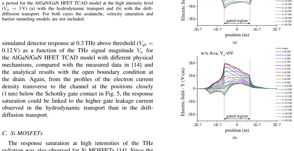
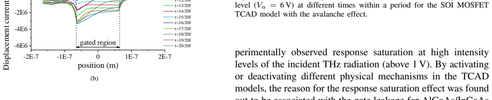
The key machinery is the mechanism-toggle TCAD experiment: the same detector structure is simulated with hydrodynamic versus drift-diffusion transport, and with velocity saturation, avalanche, and gate barrier tunneling separately included or excluded. Hydrodynamic transport is the load-bearing ingredient for the HFET result, because it accounts for energy transport across heterointerfaces and thereby produces the gate leakage current that the drift-diffusion model misses. For the silicon MOSFET, the avalanche model plays that role: switching it off removes the enhanced displacement current near the drain and largely removes the saturation. Toggling these mechanisms is what connects each predicted saturation curve to a specific physical cause.
What would settle it
Measure the drain response of the same AlGaAs/InGaAs or AlGaN/GaN detector at 0.3 THz over a wide power range without renormalizing the ordinate and compare absolute volts of response to the TCAD prediction; if the measured curve saturates at a different level than simulated, or if the simulated curve does not flatten when gate leakage is suppressed, the attributed mechanism is wrong. For the Si MOSFET, directly measuring the impact-ionization or substrate current during high-intensity illumination would test the avalanche claim.
Extended reading notes
Core claim
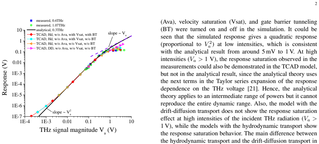
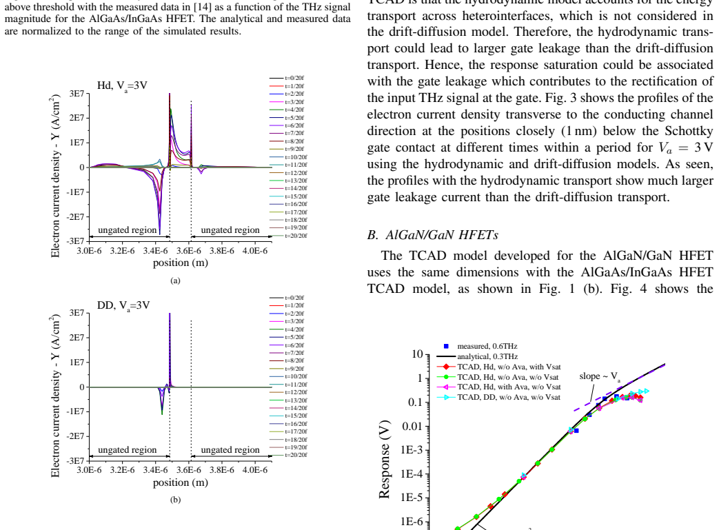
The paper's central claim is that full-device TCAD models reproduce the experimentally observed saturation of the TeraFET drain response to intense THz radiation, and that the saturation mechanism differs by material system. In the III-V HFETs, hydrodynamic transport predicts substantially larger transverse electron current below the Schottky gate than drift-diffusion transport; this gate leakage rectifies the input THz signal and flattens the response, while the drift-diffusion model fails to saturate. In the SOI MOSFET, where gate leakage is blocked by the oxide, the paper identifies the avalanche (impact ionization) model together with velocity saturation as the cause: high THz fields generate carriers that enhance the displacement current near the drain, acting like a leakage path. The analytical theory, in contrast, is limited to an intermediate power range because it uses only the next terms of a Taylor expansion.
Load-bearing premise
The validation is established by normalizing the measured and analytical curves to the range of the simulated results, and the measurements were taken at 0.6 and 1.07 THz while the simulations run at 0.3 THz, so if that normalization hides large absolute discrepancies, the mechanism attribution built on the validation is unsupported.
Editorial extensions
If this is right
- The analytical Taylor-expansion response formula is valid only over an intermediate power range and cannot reproduce high-intensity saturation, so TCAD is required for full dynamic-range TeraFET modeling.
- Hydrodynamic transport, not drift-diffusion, is necessary to capture THz response saturation in III-V HFETs, because it includes energy transport across heterointerfaces and hence the gate leakage that causes the roll-off.
- In Si MOSFETs, gate leakage is negligible, and the observed saturation is associated with avalanche-generated carriers and velocity saturation, with the gate oxide field staying below the breakdown limit.
- The mechanism-by-mechanism TCAD approach attributes saturation to different device physics in different material systems, rather than to a single universal high-power effect.
Reading between the lines
- If gate leakage is the saturation knob in III-V TeraFETs, then a detector with a higher Schottky barrier or a gate insulator should push the saturation onset to higher THz powers; this design consequence is implied by the paper's mechanism but is not tested there.
- The avalanche interpretation for the Si MOSFET predicts that the saturation threshold should depend on channel length and doping through the electric-field profile, so a series of devices with varied geometry could separate avalanche from velocity-saturation contributions experimentally.
- A hybrid modeling strategy, analytical at low and intermediate power and TCAD for the high-power regime, could yield compact models valid over the whole dynamic range; the paper points toward such models but does not build them.
Signed reviews
Editorial analysis
A structured set of objections, weighed in public.
Referee Report
Summary. The manuscript presents Synopsys Sentaurus TCAD models for three TeraFET detector types: AlGaAs/InGaAs HFETs, AlGaN/GaN HFETs, and SOI MOSFETs. The authors simulate the rectified drain response versus THz signal amplitude at 0.3 THz while toggling physical mechanisms (hydrodynamic vs. drift-diffusion transport, avalanche, velocity saturation, gate barrier tunneling) on and off. The simulated responses are compared with measured data from the literature at 0.6 and 1.07 THz and with an analytical theory. The central claim is that the saturation of the detector response at high intensities (above about 1 V) is caused by gate leakage in the two HFET material systems and by velocity saturation and avalanche effects in Si MOSFETs.
Significance. The systematic mechanism-toggling methodology is a genuine strength: it offers a transparent way to attribute a nonlinear response effect to specific physical mechanisms, and the spatially resolved current-density, electric-field, and impact-ionization profiles give mechanistic insight that goes beyond a simple circuit-level fit. If the validation were secure, the material-specific conclusions would be practically useful for high-power THz detection and for developing compact TeraFET models. However, the experimental validation as presented is weakened by vertical normalization of the measured and analytical curves to the simulated range, by the mismatch between simulated and measured frequencies, and by the use of an uncalibrated 'exemplary' Si MOSFET model. The mechanistic conclusions are plausible but are not yet established by the evidence shown.
major comments (4)
- [Figs. 2, 4, 6 captions] The captions state that 'the analytical and measured data are normalized to the range of the simulated results.' This introduces a free vertical scaling factor for every comparison curve. With this normalization, no absolute detector response is ever compared with experiment, so the abstract's claim that the models are 'validated over a wide dynamic range' and the Section III claim that the models 'explain the experimentally observed response saturation' are not supported by the data as presented. The authors should plot absolute measured and simulated responses on a common scale, or provide an independently derived calibration factor and demonstrate that it is not tuned per curve.
- [Figs. 2, 4, 6; Sections II-A, II-B, II-C] All simulations are performed at 0.3 THz, while the measured data cited from [14] were taken at 0.6 and 1.07 THz. The TeraFET response magnitude, and in particular the onset and sharpness of saturation, can depend on frequency through the plasma-wave impedance and the gate-channel coupling. Because the vertical scale is normalized, the comparison cannot reveal whether the simulated frequency dependence is correct. Please simulate at the measured frequencies or justify quantitatively that the saturation onset is frequency-independent over this range.
- [Section II-A and reference [18]] The AlGaAs/InGaAs HFET model is stated to have been 'validated' by comparing simulated I-V characteristics and the gate-bias dependence of the THz response with measured data in [18], which is listed as an unpublished conference paper. The calibration parameters and validation plots are therefore not available for inspection in this manuscript. The present paper's validation chain depends on that reference, so the essential calibration results should be included in the paper or in a supplementary document.
- [Section II-C] The Si MOSFET model is explicitly described as an 'exemplary' SOI device using default material parameter files, not calibrated to the specific measured detector from [14]. The conclusion that velocity saturation and avalanche are responsible for the Si MOSFET response saturation is therefore not tied to the measured device. A sensitivity analysis over device parameters, or calibration to the measured device's I-V and response data, is needed to support the attribution for this material system.
minor comments (5)
- [Abstract] The phrase 'AlGaAs/InGaAs and AlGaN/GaN and silicon TeraFETs' should read 'AlGaAs/InGaAs, AlGaN/GaN, and silicon TeraFETs' for clarity.
- [Figs. 2, 4, 6 legends] The legend text 'slope ~ Va s' and 'slope ~ V2 a' appears to contain formatting artifacts; these should read 'slope ~ V_a' and 'slope ~ V_a^2', respectively.
- [Section II-B] The sentence 'uses the same dimensions with the AlGaAs/InGaAs HFET TCAD model' should be 'uses the same dimensions as the AlGaAs/InGaAs HFET TCAD model.'
- [Figs. 3 and 5] The x-axis label 'position (m)' with tick values around 3.0E-6 is technically meters, but the authors should confirm whether the intended unit is micrometers and make the axis label unambiguous.
- [Reference [18]] Reference [18] is listed as 'to be published'; if it has appeared by the time of resubmission, the citation should be updated with full publication details.
Circularity Check
Central saturation mechanism is not fitted to the data, but the experimental validation is weakened by free vertical normalization and by delegating model calibration to an unpublished self-citation.
-
self citation load bearing
[Section II-A, AlGaAs/InGaAs HFETs (model validation); reference [18]]
"It has been validated by comparing the simulated I-V characteristics and the dependence of the THz response on the gate bias with the measured data and the analytical results [18]."
The claim that the TCAD models are validated rests on [18], a same-author conference paper listed as 'to be published' at the time. No external, independently checkable validation data or machine-checked proof is provided for that calibration. The HFET saturation mechanisms are then inferred from this self-cited model, making the model credibility chain depend on an unverified self-citation. The centrality is partial: the mechanism selection itself is performed by toggling physical models in this paper, not by importing [18]'s saturation result.
-
other
[Fig. 2 caption (also Figs. 4 and 6), Sections II-A, II-B, II-C]
"The analytical and measured data are normalized to the range of the simulated results."
The experimental agreement used to support the models is produced after vertically rescaling the measured and analytical curves to the simulated response range. This removes the absolute response magnitude from the comparison, so the apparent quantitative agreement is partly constructed by choosing the vertical scale to match the simulation. The saturation onset on the unnormalized horizontal Va axis is still an independent shape constraint, and the mechanism attribution follows from switching physics models on and off, so this is a partial free-scaling validation weakness rather than a full reduction of the central mechanism claim.
full rationale
The paper's central derivation is not equivalent to its inputs by construction: the high-intensity saturation behavior is obtained by activating and deactivating hydrodynamic versus drift-diffusion transport, avalanche, velocity saturation, and gate barrier tunneling in Sentaurus TCAD, and no parameter of those models is fitted to the measured high-power response of reference [14]. The analytical theory [21] is used only in the low-power quadratic regime and does not contain the saturation mechanism. The two concerns above, however, are real: the model calibration for the HFETs is delegated to the authors' own unpublished work [18], and the comparison curves are vertically normalized to the simulated range, so the empirical support for the mechanism attribution is weaker than the text implies. These are validation-dependency and free-scaling issues, not a full circular reduction; the central mechanism claim still has independent content, so the circularity score is moderate rather than high.
Assumptions & free parameters
free parameters (3)
- Measured data normalization scale =
not given (normalized to simulated range)
- Analytical data normalization scale =
not given
- TCAD calibration parameters =
not listed (from prior work [18])
assumptions (5)
- domain assumption Synopsys Sentaurus hydrodynamic and drift-diffusion transport models correctly capture THz device behavior.
- domain assumption The analytical TeraFET response theory of [21] is valid at low and intermediate intensities.
- domain assumption The experimental data of [14] are accurate and representative.
- domain assumption Turning each physical mechanism on or off in TCAD isolates its contribution without hidden coupling.
- domain assumption The AlGaN/GaN HFET can be modeled with the same dimensions as the AlGaAs/InGaAs HFET.
Cite this review
Pith. "Pith review of TCAD model for TeraFET detectors operating in a large dynamic range." pith.science (2026). https://pith.science/paper/CR6J2PWX
@misc{pith2026190804845,
  author       = {Pith},
  title        = {Pith review of: TCAD model for TeraFET detectors operating in a large dynamic range},
  year         = {2026},
  howpublished = {\url{https://pith.science/paper/CR6J2PWX}},
  note         = {Machine review of arXiv:1908.04845}
}
read the original abstract
We present technology computer-aided design (TCAD) models for AlGaAs/InGaAs and AlGaN/GaN and silicon TeraFETs, plasmonic field effect transistors (FETs), for terahertz (THz) detection validated over a wide dynamic range. The modeling results are in good agreement with the experimental data for the AlGaAs/InGaAs heterostructure FETs (HFETs) and, to the low end of the dynamic range, with the analytical theory of the TeraFET detectors. The models incorporate the response saturation effect at high intensities of the THz radiation observed in experiments and reveal the physics of the response saturation associated with different mechanisms for different material systems. These mechanisms include the gate leakage, the velocity saturation and the avalanche effect.
Figures

Figures from the paper (5 more)



Reference graph
Works this paper leans on
-
[18]
An efficient TCAD model for TeraFET detectors,
X. Liu and M. Shur, “An efficient TCAD model for TeraFET detectors,” in 2019 IEEE Radio and Wirel. Symp. (RWS) , Orlando, FL, USA, Jan. 2019, to be published
work page 2019
-
[14]
The dynamic range of THz broadband FET detectors,
D. B. But et al., “The dynamic range of THz broadband FET detectors,” in Proc. SPIE, Terahertz Emitters, Receivers, and Applications IV , San Diego, CA, USA, Sep. 2013, vol. 8846, Art. no. 884612
work page 2013
-
[1]
M. Dyakonov and M. S. Shur, “Shallow water analogy for a ballistic field effect transistor: New mechanism of plasma wave generation by dc current,” Phys. Rev. Lett., vol. 71, no. 15, pp. 2465–2468, Oct. 1993
work page 1993
-
[2]
M. I. Dyakonov and M. S. Shur, “Detection, mixing, and frequency mul- tiplication of terahertz radiation by two-dimensional electronic fluid,” IEEE Trans. Electron Devices , vol. 43, no. 3, pp. 380–387, Mar. 1996
work page 1996
-
[3]
Plasma wave electronics: novel terahertz devices using two-dimensional electron fluid,
M. I. Dyakonov and M. S. Shur, “Plasma wave electronics: novel terahertz devices using two-dimensional electron fluid,” IEEE Trans. Electron Devices, vol. 43, no. 10, pp. 1640–1645, Oct. 1996
work page 1996
-
[4]
H. Marinchio et al. , “Room-temperature terahertz mixer based on the simultaneous electronic and optical excitations of plasma waves in a field effect transistor,” Appl. Phys. Lett., vol. 96, no. 1, pp. 013502, Jan. 2010
work page 2010
-
[5]
Terahertz detection by a homodyne field effect transistor multiplicative mixer,
S. Preu et al., “Terahertz detection by a homodyne field effect transistor multiplicative mixer,” IEEE Trans. Terahertz Sci. Technol., vol. 2, no. 3, pp. 278–283, May 2012
work page 2012
-
[6]
K. Wu, S. Muralidharan, and M. M. Hella, “A Wideband SiGe BiCMOS Frequency Doubler with 6.5-dBm Peak Output Power for Millimeter- Wave Signal Sources,” IEEE Trans. Microw. Theory Tech., vol. 86, no. 3, pp. 187–200, Jan. 2018
work page 2018
Show all 21 references
-
[7]
A 165-230GHz SiGe amplifier- doubler chain with 5dBm peak output power,
S. Muralidharan, K. Wu, and M. Hella, “A 165-230GHz SiGe amplifier- doubler chain with 5dBm peak output power,” in IEEE RFIC Sympo- sium, San Francisco, CA, USA, 2016, pp. 302–305
2016
-
[8]
A 216GHz 0.5 mW transmitter with a compact power combiner in 65nm CMOS,
S. Muralidharan, K. Wu, and M. Hella, “A 216GHz 0.5 mW transmitter with a compact power combiner in 65nm CMOS,” in Microwave Conference (APMC), 2015 Asia-Pacific , vol. 2, pp. 1–3, Dec. 2015
2015
-
[9]
A 220 GHz OOK Outphasing Transmit- ter in 130-nm BiCMOS Technology,
K. Wu, B. Fahs, and M. Hella, “A 220 GHz OOK Outphasing Transmit- ter in 130-nm BiCMOS Technology,” 2018 IEEE BiCMOS and Com- pound Semiconductor Integrated Circuits and Technology Symposium (BCICTS), pp. 227–230, Oct. 2018
2018
-
[10]
Field effect transistors for terahertz detection: Physics and first imaging applications,
W. Knap et al., “Field effect transistors for terahertz detection: Physics and first imaging applications,” J. Infrared Millim. Terahertz Waves, vol. 30, no. 12, pp. 1319–1337, Dec. 2009. 5
2009
-
[11]
Exploration of terahertz imaging with silicon MOSFETs,
A. Lisauskas et al. , “Exploration of terahertz imaging with silicon MOSFETs,” J. Infrared Millim. Terahertz Waves , vol. 35, no. 1, pp. 63–80, Jan. 2014
2014
-
[12]
Terahertz vision using field effect transistors detectors arrays,
N. Dyakonova et al. , “Terahertz vision using field effect transistors detectors arrays,” in 2018 22nd International Microwave and Radar Conference (MIKON), pp. 711–714, May 2018
2018
-
[13]
THz autocorrelators for ps pulse characterization based on Schottky diodes and rectifying field-effect transistors,
S. Preu, M. Mittendorff, S. Winnerl, O. Cojocari, and A. Penirschke, “THz autocorrelators for ps pulse characterization based on Schottky diodes and rectifying field-effect transistors,” IEEE Trans. Terahertz Sci. Technol., vol. 5, no. 6, pp. 922–929, Nov. 2015
2015
-
[15]
Nonlinear photoresponse of field effect transistors terahertz detectors at high irradiation intensities,
D. B. But et al. , “Nonlinear photoresponse of field effect transistors terahertz detectors at high irradiation intensities,” J. Appl. Phys. , vol. 115, no. 16, Apr. 2014, Art. no. 164514
2014
-
[16]
Saturation of photoresponse to intense THz radiation in AlGaN/GaN HEMT detector,
N. Dyakonova et al. , “Saturation of photoresponse to intense THz radiation in AlGaN/GaN HEMT detector,” J. Appl. Phys. , vol. 120, no. 16, Oct. 2016, Art. no. 164507
2016
-
[17]
AlGaN/GaN HEMTs photoresponse to high intensity THz radiation,
N. Dyakonova et al. , “AlGaN/GaN HEMTs photoresponse to high intensity THz radiation,” Opto-Electron. Rev., vol. 23, no. 3, pp. 195– 199, Sep. 2015
2015
-
[19]
Sentaurus Device User Guide (Version N-2017.09), Synopsys Inc., Mountain View, CA, USA, 2017
2017
-
[20]
A High- Performance 0.13-m AlGaAs/InGaAs pHEMT Process Using Sidewall Spacer Technology,
A. T. Ping, W. Liebl, G. Mahoney, S. Mahon, and O. Berger, “A High- Performance 0.13-m AlGaAs/InGaAs pHEMT Process Using Sidewall Spacer Technology,” in 2005 GaAs MANTECH Dig. , Apr. 2005
2005
-
[21]
Plasmonic terahertz detector response at high intensities,
A. Gutin, V . Kachorovskii, A. Muraviev, and M. Shur, “Plasmonic terahertz detector response at high intensities,” J. Appl. Phys. , vol. 112, no. 1, Jul. 2012, Art. no. 014508
2012
Reviewed August 14, 2026 · model on record in the stance chip above.
Discussion (0). Continue with ORCID to comment.