REVIEW 1 major objections 5 minor 76 references
Multiple Andreev reflections and Shapiro steps in a Ge-Si nanowire Josephson junction
T0 review · 1 major / 5 minor · reviewed 2026-08-14 · deepseek-v4-flash
Pith's one-line read Ge-Si nanowire junction confirmed as a true Josephson junction
desk verdict A clean, honest device paper with solid dc/ac Josephson and MAR data, but the ballistic-limit and transparency estimates rest on assumed parameters and should be softened. read the letter →
The pith
A machine-rendered reading of the paper's core claim, the machinery that carries it, and where it could break.
The reading
What carries the argument
The central object is the Josephson junction itself: a semiconducting Ge-Si island of about 50 nm between aluminum leads, formed by thermal annealing that drives aluminum interdiffusion. Three observable signatures carry the argument: the switching and retrapping currents for the dc Josephson effect; the Shapiro-step condition $V = m h f/2e$ for the ac Josephson effect; and the multiple-Andreev-reflection condition $eV = 2\Delta_{\mathrm{Al}}/n$. The fit of the critical current versus temperature by the Galaktionov-Zaikin ballistic model supplies the interface transparency and mode-count estimates.
What would settle it
Measure the switching current of a series of devices with identical processing but semiconducting island lengths from about 50 nm to a few hundred nanometers: a ballistically behaving junction should keep the switching current near the per-mode limit and retain high-order Andreev peaks, whereas a diffusive junction should show the switching current suppressed by orders of magnitude and the Andreev peaks washed out beyond second order.
Extended reading notes
Core claim
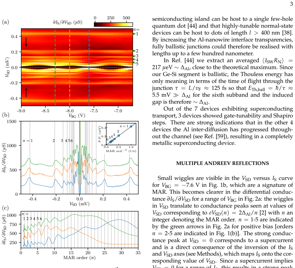
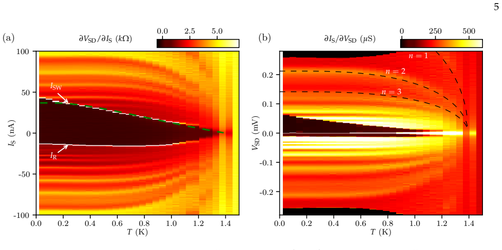
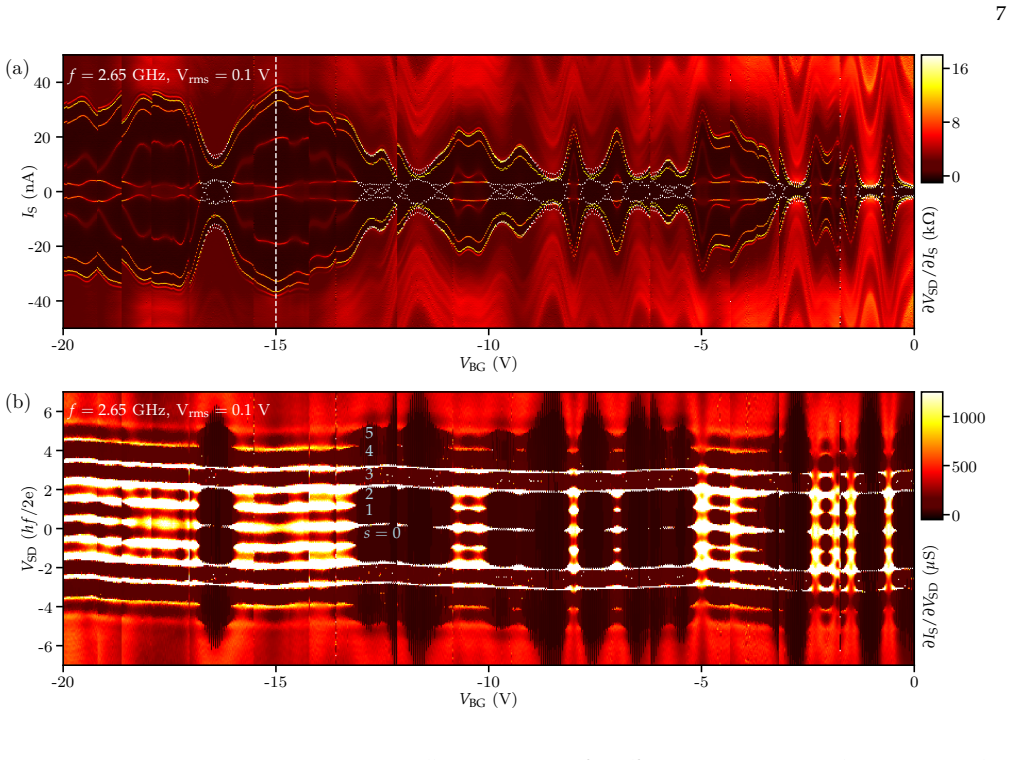
The central claim is that a Ge-Si core-shell nanowire contacted by aluminum forms a true, well-behaved Josephson junction. The dc effect appears as a finite switching current of tens of nanoamps with hysteretic retrapping; the ac effect appears as current plateaus at voltages $m h f/2e$, observed up to $m = 23$. Conductance peaks at biases $2\Delta_{\mathrm{Al}}/n$ for $n = 1\dots 6$ locate multiple Andreev reflections, which the authors interpret as quasiparticles traversing the roughly 50 nm semiconducting island elastically at least six times. Fitting the temperature dependence of the critical current with a ballistic model yields an average interface transparency around 50%, and the superconducting gap extracted from the Andreev peak positions matches an aluminum critical temperature of about 1.4 K.
Load-bearing premise
The load-bearing premise is that charge carriers cross the semiconducting island without scattering inside it; this is inferred from an estimated elastic mean free path of 100 to 400 nm, so if the actual mean free path were much shorter, the junction would be diffusive and the fitted transparency and mode counts would no longer stand.
Editorial extensions
If this is right
- The device can serve as a building block for Majorana bound state experiments in Ge-Si nanowires, a material system where induced superconductivity had been little explored.
- Because the island is estimated to be ballistic with 50% to 80% transparent interfaces, improved contacts could yield fully ballistic junctions with critical currents near the theoretical per-mode limit.
- The demonstrated gate tunability of the switching current and Shapiro steps enables in-situ control of junction properties, useful for transmon, gatemon, and Andreev spin qubits.
- The multiple Andreev reflections up to sixth order provide a direct spectroscopic measure of the aluminum gap and its temperature dependence, matching an independent measurement of the aluminum critical temperature.
- The observation of both the dc and ac Josephson effects in the same device establishes a quality benchmark for future superconductor-nanowire junctions in this platform.
Reading between the lines
- If the ballistic interpretation is correct, a length-dependence test should hold: devices with longer semiconducting islands should show a sharply suppressed switching current and washed-out high-order Andreev peaks, while 50 nm islands should retain them.
- The spread between the 50% transparency from the ballistic critical-current fit and the 80% from the earlier BTK analysis suggests that most scattering sits at the aluminum-germanium interfaces rather than inside the channel, a hypothesis that could be tested by varying the contact annealing recipe.
- The clean sixth-order Andreev reflections and 23 Shapiro steps could be used as an experimental quality metric for other semiconductor-superconductor nanowire platforms aiming at topological physics.
- Because high-order Andreev reflections are sensitive to inelastic scattering, tracking the maximum resolvable order as a function of temperature and gate voltage could probe decoherence inside the junction without needing a separate quantum dot device.
Signed reviews
Editorial analysis
A structured set of objections, weighed in public.
Referee Report
Summary. The manuscript reports a Ge-Si core-shell nanowire Josephson junction with superconducting Al contacts. The authors demonstrate the dc Josephson effect through a finite, gate-tunable switching current with hysteretic retrapping, observe multiple Andreev reflection (MAR) conductance peaks up to sixth order, extract a superconducting gap ΔAl = 0.212 meV from the MAR peak positions, compare the temperature dependence of the switching current with a ballistic Eilenberger-model calculation, and show Shapiro steps up to m = 23 under microwave irradiation. They conclude that the junction is a true Josephson junction with transparent, low-disorder interfaces and estimate the transparency at 50–80% and the semiconducting segment to be ballistic.
Significance. The experimental signatures are standard and convincingly presented: the supercurrent, the MAR peak positions following eV = 2Δ/n, the Shapiro step heights following ΔV = hf/2e, and the BCS-like temperature dependence are mutually consistent, and the extracted Tc is independently confirmed by the critical temperature of an Al strip. If these results stand, they establish the Ge-Si nanowire platform for hybrid superconductor-semiconductor devices, which is relevant for proposals involving Majorana bound states, transmon/gatemon qubits, and Andreev (spin) qubits. The data are carefully measured with due attention to hysteresis and axis-inversion artifacts in the post-processing. The weakest link is the quantitative transport classification (ballistic vs diffusive), which is load-bearing for the transparency estimate but not for the central existence of the Josephson effect.
major comments (1)
- [Junction characteristics; Temperature dependence of ISW and MAR] The classification of the semiconducting island as ballistic is not robust. The elastic mean free path le is estimated as 100–400 nm from assumed mobility μ ≈ 3500 cm2/Vs, effective mass m* ≈ 0.5 me, and gate lever arm α = 0.02; for a semiconducting island of L ≈ 50 nm this gives le/L ≈ 2–8, which does not convincingly satisfy the stated criterion le >> L, and at the lower end le is comparable to L and to the diffusive coherence length. Because the Galaktionov–Zaikin model used to fit Ic(T) in the temperature-dependence section assumes ballistic transport, the extracted average transparency of ~50% and the ~7 modes inherit this uncertainty; if the true le is shorter, the junction is quasi-diffusive and the fit is not the correct model. The text itself only says the device 'approach[es] the ballistic limit,' whereas the conclusion states that the nanowire segment 'is in the ballistic limit.' Please either temper the quantitative transparency/ballistic claims or provide an independent check (for example, normal-state conductance quantization, or comparison with a diffusive MAR model).
minor comments (5)
- [Temperature dependence of ISW and MAR, Eq. (1)] The text states 'ΔAl,0 = 0.212 µeV'; this should read 0.212 meV. In addition, the prefactor '2ΔAl,0/n' in Eq. (1) should be defined, since for n = 2 it reduces to ΔAl,0.
- [Introduction; Methods] The introduction says the device was designed for 4-terminal measurements, but the Methods section states 'All measurements in this work are performed using a 3-probe measurement.' Please clarify this discrepancy.
- [Fig. 2b and inset] The inset axis label 'MAR ord. −1 (1/n)' is confusing, and 'P.P.' is not defined before use. Please spell out 'peak position' and clarify the axis labels.
- [Multiple Andreev reflections] The sentence 'This is confirmed by an independent measurement of the TC of an Al stripline (not shown)' is not verifiable as written; please include the data or provide a reference to a methods description.
- [Throughout] There are several typographical and encoding artifacts, including 'devicesâ ˘A ´Z surroundings' in the temperature-dependence section, an incomplete parenthetical in the Fig. 2 caption, and the incomplete reference [24] 'Mergenthaler et al., 1 (2019)'. These should be corrected.
Circularity Check
Mild self-definitional step: ΔAl is fitted from MAR peak positions and then reused to compute expected MAR positions and label MAR orders; otherwise the paper is anchored by independent Shapiro-step and Tc checks.
-
self definitional
[Section 'Multiple Andreev reflections', Fig. 2b inset and Fig. 2c]
"For a more accurate estimate of ∆Al we perform a linear fit through zero for the six MAR peak positions and find ∆Al = 0.212 meV ... Vertical grey dashed lines denote expected MAR peak positions calculated by n = 2∆Al/eVSD ... In Fig. 2c, we therefore convert the x-axis from VSD to units of n = 2∆Al/eVSD."
The ΔAl value used to draw the expected MAR positions and to convert the x-axis into MAR order n is not independent: it was obtained by a linear fit through zero to those same six MAR peak positions via P.P. = 2ΔAl/n. After the conversion, peaks near integer n are aligned largely by construction of the fit, so the visual 'match' of the blue curve to integer n up to 6 is partly tautological. The same fitted ΔAl,0 is then inserted into Eq. (1) to claim agreement with the n=2 MAR peak in Fig. 3b. This is mild because the peaks genuinely exist, the fit has small residuals, and the paper provides an independent Al stripline Tc measurement and a BCS temperature-shape check; the Shapiro-step and true-Josephson-junction conclusions do not depend on this step.
full rationale
The only identifiable circular chain is the reuse of the MAR-fitted ΔAl to compute expected MAR positions and to assign MAR order n, including the BCS curve in Fig. 3b. This is a self-definitional presentation step rather than a fabricated prediction: the raw conductance peaks in Fig. 2a are direct data, the linear fit through zero is a standard way to extract ΔAl, and the paper independently confirms ΔAl with the measured Tc of an Al stripline and the observed disappearance of ISW near 1.4 K. The ac Josephson claim is checked against the parameter-free relation ΔV = hf/2e with up to 23 steps, which is not derived from any fitted quantity. The Ic(T) fit uses the externally published Galaktionov-Zaikin model with stated inputs (Tc = 1.4 K, vF = 1×10^5 m/s, electrode separation 50 nm) and outputs transparency and mode count; this is a model fit, not a renamed input. The ballistic-limit estimate is assumption-dependent (mobility, effective mass, lever arm), but it is a quantitative estimate, not a circular derivation. Self-citations such as Refs. [38], [44], and [59] supply prior device characterization and are not used as an unverified uniqueness theorem. Overall, the paper's central observations and their external checks are self-contained, with only the moderate MAR-labeling circularity described above.
Assumptions & free parameters
free parameters (4)
- Superconducting gap ΔAl,0 =
0.212 meV
- Effective hole mass m* =
0.5 m_e
- Hole mobility μ =
3500 cm^2/Vs (at 4 K)
- Gate lever arm α =
0.02
assumptions (5)
- domain assumption The superconducting gap of the aluminum leads is the only energy scale for MAR peak positions, with eV = 2Δ/n.
- domain assumption The Eilenberger-based Galaktionov-Zaikin model describes the temperature dependence of the critical current in this junction.
- domain assumption The semiconducting island is ~50 nm long and can be modeled as a cylindrical potential well to estimate Fermi energies.
- domain assumption The series resistance of 3.46 kΩ is accurately subtracted from all measurements.
- domain assumption The BCS temperature dependence with a modified prefactor 2Δ_0/n (Eq. 1) describes the MAR peak positions versus temperature.
Cite this review
Pith. "Pith review of Multiple Andreev reflections and Shapiro steps in a Ge-Si nanowire Josephson junction." pith.science (2026). https://pith.science/paper/D57Q26ZS
@misc{pith2026190807579,
  author       = {Pith},
  title        = {Pith review of: Multiple Andreev reflections and Shapiro steps in a Ge-Si nanowire Josephson junction},
  year         = {2026},
  howpublished = {\url{https://pith.science/paper/D57Q26ZS}},
  note         = {Machine review of arXiv:1908.07579}
}
read the original abstract
We present a Josephson junction based on a Ge-Si core-shell nanowire with transparent superconducting Al contacts, a building block which could be of considerable interest for investigating Majorana bound states, superconducting qubits and Andreev (spin) qubits. We demonstrate the dc Josephson effect in the form of a finite supercurrent through the junction, and establish the ac Josephson effect by showing up to 23 Shapiro steps. We observe multiple Andreev reflections up to the sixth order, indicating that charges can scatter elastically many times inside our junction, and that our interfaces between superconductor and semiconductor are transparent and have low disorder.
Figures

Figures from the paper (2 more)

Reference graph
Works this paper leans on
-
[1]
B. D. Josephson, Physics Letters 1, 251 (1962)
1962
-
[2]
M. Tinkham, Introduction to Superconductivity Second Edi- tion (Dover Publications, Inc., Mineola, New York, 2004). 8
work page 2004
-
[3]
Shapiro, Physical Review Letters 11, 80 (1963)
S. Shapiro, Physical Review Letters 11, 80 (1963)
work page 1963
-
[4]
C. C. Grimes and S. Shapiro, Physical Review 169, 397 (1968)
work page 1968
-
[5]
K. K. Likharev, Reviews of Modern Physics51, 101 (1979)
work page 1979
-
[6]
C. W. J. Beenakker, Physical Review B 46, 12841 (1992)
work page 1992
-
[7]
E. N. Grossman, IEEE Transactions on Microwave Theory and Techniques 42, 707 (1994)
work page 1994
-
[8]
I. V . Krive, S. I. Kulinich, R. I. Shekhter, and M. Jonson, Low Temperature Physics 30, 554 (2004)
work page 2004
Show all 76 references
-
[9]
Jarillo-Herrero, J
P . Jarillo-Herrero, J. A. van Dam, and L. P . Kouwenhoven, Nature 439, 953 (2006)
2006
-
[10]
Katsaros, P
G. Katsaros, P . Spathis, M. Stoffel, F. Fournel, M. Mongillo, V . Bouchiat, F. Lefloch, A. Rastelli, O. G. Schmidt, and S. De Franceschi, Nature nanotechnology 5, 458 (2010)
2010
-
[11]
Mizuno, B
N. Mizuno, B. Nielsen, and X. Du, Nature communica- tions 4, 2716 (2013)
2013
-
[12]
J. C. Estrada Saldaña, R. Žitko, J. P . Cleuziou, E. J. H. Lee, V . Zannier, D. Ercolani, L. Sorba, R. Aguado, and S. De Franceschi, Science Advances 5, eaav1235 (2019)
2019
-
[13]
N. W. Hendrickx, D. P . Franke, A. Sammak, M. Kouwen- hoven, D. Sabbagh, L. Yeoh, R. Li, M. L. V . Tagliaferri, M. Virgilio, G. Capellini, G. Scappucci, and M. Veldhorst, Nature Communications 9, 2835 (2018)
2018
-
[14]
Kim, B.-K
H.-S. Kim, B.-K. Kim, Y. Yang, X. Peng, S.-G. Lee, D. Yu, and Y.-J. Doh, Applied Physics Express9, 023102 (2016)
2016
-
[15]
Cleuziou, W
J. Cleuziou, W. Wernsdorfer, V . Bouchiat, T. Ondarçuhu, and M. Monthioux, Nature Nanotechnology 1, 53 (2006)
2006
-
[16]
Vigneau, R
F. Vigneau, R. Mizokuchi, D. C. Zanuz, X. Huang, S. Tan, R. Maurand, S. Frolov, A. Sammak, G. Scappucci, F. Lefloch, and S. De Franceschi, Nano Letters 19, 1023 (2019)
2019
-
[17]
J. A. van Dam, Y. V . Nazarov, E. P . A. M. Bakkers, S. De Franceschi, and L. P . Kouwenhoven, Nature 442, 667 (2006)
2006
-
[18]
H. I. Jørgensen, T. Novotný, K. Grove-Rasmussen, K. Flensberg, and P . E. Lindelof, Nano Letters 7, 2441 (2007)
2007
-
[19]
Delagrange, R
R. Delagrange, R. Weil, A. Kasumov, M. Ferrier, H. Bouch- iat, and R. Deblock, Physica B: Condensed Matter 536, 211 (2018)
2018
-
[20]
Hofstetter, S
L. Hofstetter, S. Csonka, J. Nygard, and C. Schonen- berger, Nature 461, 960 (2009)
2009
-
[21]
Z. B. Tan, D. Cox, T. Nieminen, P . Lähteenmäki, D. Gol- ubev, G. B. Lesovik, and P . J. Hakonen, Physical Review Letters 114, 096602 (2015)
2015
-
[22]
de Lange, B
G. de Lange, B. van Heck, A. Bruno, D. J. van Woerkom, A. Geresdi, S. R. Plissard, E. P . A. M. Bakkers, A. R. Akhmerov, and L. DiCarlo, Physical Review Letters 115, 127002 (2015)
2015
-
[23]
T. W. Larsen, K. D. Petersson, F. Kuemmeth, T. S. Jes- persen, P . Krogstrup, J. Nygård, and C. M. Marcus, Phys- ical Review Letters 115, 127001 (2015)
2015
-
[24]
Mergenthaler, A
M. Mergenthaler, A. Nersisyan, A. Patterson, M. Esposito, A. Baumgartner, C. Schönenberger, G. A. D. Briggs, E. A. Laird, and P . J. Leek, 1 (2019)
2019
-
[25]
J. G. Kroll, W. Uilhoorn, K. L. van der Enden, D. de Jong, K. Watanabe, T. Taniguchi, S. Goswami, M. C. Cassidy, and L. P . Kouwenhoven, Nature Communications9, 4615 (2018)
2018
-
[26]
Casparis, M
L. Casparis, M. R. Connolly, M. Kjaergaard, N. J. Pear- son, A. Kringhøj, T. W. Larsen, F. Kuemmeth, T. Wang, C. Thomas, S. Gronin, G. C. Gardner, M. J. Manfra, C. M. Marcus, and K. D. Petersson, Nature Nanotechnology 13, 915 (2018)
2018
-
[27]
A. Y. Kitaev, Physics-Uspekhi 44, 131 (2001)
2001
-
[28]
Mourik, K
V . Mourik, K. Zuo, S. M. Frolov, S. R. Plissard, E. P . A. M. Bakkers, and L. P . Kouwenhoven, Science336, 1003 (2012)
2012
-
[29]
M. T. Deng, S. VaitiekÄ ˚Unas, E. B. Hansen, J. Danon, M. Leijnse, K. Flensberg, J. Nygård, P . Krogstrup, and C. M. Marcus, Science 354, 1557 (2016)
2016
-
[30]
Aguado, Rivista del Nuovo Cimento 40, 523 (2017)
R. Aguado, Rivista del Nuovo Cimento 40, 523 (2017)
2017
-
[31]
R. M. Lutchyn, E. P . A. M. Bakkers, L. P . Kouwenhoven, P . Krogstrup, C. M. Marcus, and Y. Oreg, Nature Reviews Materials 3, 52 (2018)
2018
-
[32]
Ö. Gül, H. Zhang, J. D. S. Bommer, M. W. A. de Moor, D. Car, S. R. Plissard, E. P . A. M. Bakkers, A. Geresdi, K. Watanabe, T. Taniguchi, and L. P . Kouwenhoven, Na- ture Nanotechnology 13, 192 (2018)
2018
-
[33]
Y. Hu, H. O. H. Churchill, D. J. Reilly, J. Xiang, C. M. Lieber, and C. M. Marcus, Nature Nanotechnology 2, 622 (2007)
2007
-
[34]
Y. Hu, F. Kuemmeth, C. M. Lieber, and C. M. Marcus, Nature nanotechnology 7, 47 (2012)
2012
-
[35]
A. P . Higginbotham, F. Kuemmeth, M. P . Hanson, A. C. Gossard, and C. M. Marcus, Physical Review Letters 112, 026801 (2014)
2014
-
[36]
A. P . Higginbotham, T. W. Larsen, J. Yao, H. Yan, C. M. Lieber, C. M. Marcus, and F. Kuemmeth, Nano Letters 14, 3582 (2014)
2014
-
[37]
Brauns, J
M. Brauns, J. Ridderbos, A. Li, E. P . A. M. Bakkers, and F. A. Zwanenburg, Physical Review B 93, 121408(R) (2016)
2016
-
[38]
Brauns, J
M. Brauns, J. Ridderbos, A. Li, W. G. van der Wiel, E. P . A. M. Bakkers, and F. A. Zwanenburg, Applied Physics Letters 109, 143113 (2016)
2016
-
[39]
Brauns, J
M. Brauns, J. Ridderbos, A. Li, E. P . A. M. Bakkers, W. G. van der Wiel, and F. A. Zwanenburg, Physical Review B 94, 041411(R) (2016)
2016
-
[40]
Zarassi, Z
A. Zarassi, Z. Su, J. Danon, J. Schwenderling, M. Hoce- var, B. M. Nguyen, J. Yoo, S. A. Dayeh, and S. M. Frolov, Physical Review B 95, 155416 (2017)
2017
-
[41]
F. N. M. Froning, M. K. Rehmann, J. Ridderbos, M. Brauns, F. A. Zwanenburg, A. Li, E. P . A. M. Bakkers, D. M. Zumbühl, and F. R. Braakman, Applied Physics Letters 113, 073102 (2018)
2018
-
[42]
Xiang, W
J. Xiang, W. Lu, Y. Hu, Y. Wu, H. Yan, and C. M. Lieber, Nature 441, 489 (2006)
2006
-
[43]
Z. Su, A. Zarassi, B.-M. Nguyen, J. Yoo, S. A. Dayeh, and S. M. Frolov, arXiv:1610.03010 (2016)
2016 arXiv
-
[44]
Ridderbos, M
J. Ridderbos, M. Brauns, J. Shen, F. K. de Vries, A. Li, E. P . A. M. Bakkers, A. Brinkman, and F. A. Zwanenburg, Ad- vanced Materials 30, 1802257 (2018)
2018
-
[45]
F. K. de Vries, J. Shen, R. J. Skolasinski, M. P . Nowak, D. Varjas, L. Wang, M. Wimmer, J. Ridderbos, F. A. Zwa- nenburg, A. Li, S. Koelling, M. A. Verheijen, E. P . A. M. Bakkers, and L. P . Kouwenhoven, Nano Letters 18, 6483 (2018)
2018
-
[46]
Maier, J
F. Maier, J. Klinovaja, and D. Loss, Physical Review B 90, 195421 (2014)
2014
-
[47]
N. M. Chtchelkatchev and Y. V . Nazarov, Physical Review Letters 90, 226806 (2003)
2003
-
[48]
Zazunov, V
A. Zazunov, V . S. Shumeiko, E. N. Bratus’, J. Lantz, and G. Wendin, Physical Review Letters 90, 087003 (2003)
2003
-
[49]
Padurariu and Y
C. Padurariu and Y. V . Nazarov, Physical Review B 81, 144519 (2010). 9
2010
-
[50]
Janvier, L
C. Janvier, L. Tosi, L. Bretheau, Ç. Ö. Girit, M. Stern, P . Bertet, P . Joyez, D. Vion, D. Esteve, M. F. Goffman, H. Pothier, and C. Urbina, Science 349, 1199 (2015)
2015
-
[51]
D. J. van Woerkom, A. Proutski, B. van Heck, D. Bouman, J. I. Väyrynen, L. I. Glazman, P . Krogstrup, J. Nygård, L. P . Kouwenhoven, and A. Geresdi, Nature Physics 13, 876 (2017)
2017
-
[52]
M. Hays, G. de Lange, K. Serniak, D. J. van Woerkom, D. Bouman, P . Krogstrup, J. Nygård, A. Geresdi, and M. H. Devoret, Physical Review Letters 121, 047001 (2018)
2018
-
[53]
L. Tosi, C. Metzger, M. F. Goffman, C. Urbina, H. Pothier, S. Park, A. L. Yeyati, J. Nygård, and P . Krogstrup, Physi- cal Review X 9, 011010 (2019)
2019
-
[54]
Kloeffel, M
C. Kloeffel, M. Trif, and D. Loss, Physical Review B 84, 195314 (2011)
2011
-
[55]
A. P . Higginbotham, F. Kuemmeth, T. W. Larsen, M. Fitz- patrick, J. Yao, H. Yan, C. M. Lieber, and C. M. Marcus, Physical Review Letters 112, 216806 (2014)
2014
-
[56]
K. M. Itoh, J. Kato, M. Uemura, A. K. Kaliteevskii, O. N. Godisov, G. G. Devyatych, A. D. Bulanov, A. V . Gusev, I. D. Kovalev, P . G. Sennikov, H.-J. Pohl, N. V . Abrosimov, and H. Riemann, Japanese Journal of Applied Physics 42, 6248 (2003)
2003
-
[57]
Kuhlmann, U
M. Kuhlmann, U. Zimmermann, D. Dikin, S. Abens, K. Keck, and V . M. Dmitriev, Zeitschrift für Physik B Con- densed Matter 96, 13 (1994)
1994
-
[58]
Flensberg and J
K. Flensberg and J. B. Hansen, Physical Review B 40, 8693 (1989)
1989
-
[59]
Ridderbos, M
J. Ridderbos, M. Brauns, J. Shen, F. K. de Vries, A. Li, S. Kölling, M. A. Verheijen, A. Brinkman, W. G. van der Wiel, E. P . A. M. Bakkers, and F. A. Zwanenburg, arXiv:1907.05510 (2019)
2019 arXiv
-
[60]
W. C. Stewart, Applied Physics Letters 12, 277 (1968)
1968
-
[61]
X. Du, I. Skachko, and E. Y. Andrei, Physical Review B 77, 184507 (2008)
2008
-
[62]
Xiang, A
J. Xiang, A. Vidan, M. Tinkham, R. M. Westervelt, and C. M. Lieber, Nature Nanotechnology 1, 208 (2006)
2006
-
[63]
J. H. Davies, The physics of low-dimensional semiconductors (Cambridge University, New York, 1998)
1998
-
[64]
Conesa-Boj, A
S. Conesa-Boj, A. Li, S. Koelling, M. Brauns, J. Ridderbos, T. T. Nguyen, M. A. Verheijen, P . M. Koenraad, F. A. Zwa- nenburg, and E. P . A. M. Bakkers, Nano Letters 17, 2259 (2017)
2017
-
[65]
Maier, T
F. Maier, T. Meng, and D. Loss, Physical Review B 90, 155437 (2014)
2014
-
[66]
D. J. Griffiths, Introduction to Quantum Mechanics (Cam- bridge University Press, 1996)
1996
-
[67]
H. A. Nilsson, P . Samuelsson, P . Caroff, and H. Q. Xu, Nano Letters 12, 228 (2012)
2012
-
[68]
M. R. Buitelaar, W. Belzig, T. Nussbaumer, B. Babi´ c, C. Bruder, and C. Schönenberger, Physical Review Let- ters 91, 057005 (2003)
2003
-
[69]
Flensberg, J
K. Flensberg, J. B. Hansen, and M. Octavio, Physical Re- view B 38, 8707 (1988)
1988
-
[70]
A. V . Galaktionov and A. D. Zaikin, Physical Review B65, 184507 (2002)
2002
-
[71]
G. E. Blonder, M. Tinkham, and T. M. Klapwijk, Physical Review B 25, 4515 (1982)
1982
-
[72]
Senapati, M
K. Senapati, M. G. Blamire, and Z. H. Barber, Nature Ma- terials 10, 849 (2011)
2011
-
[73]
Kajimura and H
K. Kajimura and H. Hayakawa, Advances in Superconduc- tivity III: Proceedings of the 3rd International Symposium on Superconductivity (ISS ’90), November 6â ˘A¸ S9, 1990, Sendai (Springer Japan, 2012) p. 1320
1990
-
[74]
Shapiro, A
S. Shapiro, A. R. Janus, and S. Holly, Reviews of Modern Physics 36, 223 (1964)
1964
-
[75]
Gross and A
R. Gross and A. Marx, Applied superconductivity,, Vol. 1 (2005) p. 480
2005
-
[76]
Russer, Journal of Applied Physics43, 2008 (1972)
P . Russer, Journal of Applied Physics43, 2008 (1972)
1972
Reviewed August 14, 2026 · model on record in the stance chip above.
Discussion (0). Continue with ORCID to comment.