REVIEW 3 major objections 5 minor 81 references
Effect of mechanical strain on the optical properties of nodal-line semimetal ZrSiS
T0 review · 3 major / 5 minor · reviewed 2026-08-14 · deepseek-v4-flash
Pith's one-line read ZrSiS, a layered nodal-line semimetal, keeps its flat infrared conductivity under compression up to 10 GPa, undergoes a Lifshitz transition near 2 GPa tension that lowers infrared spectral weight, and hosts low-loss ~20 eV plasmons whose…
desk verdict A solid, well-calibrated DFT+RPA study with interesting strain predictions, but the headline Lifshitz-transition stress is internally inconsistent and rests on meV-scale band physics the method doesn't anchor. read the letter →
The pith
A machine-rendered reading of the paper's core claim, the machinery that carries it, and where it could break.
The reading
What carries the argument
The argument is carried by the wave-vector- and frequency-dependent dielectric function computed in the random phase approximation from first-principles band structures, with interband transitions treated from dipole matrix elements in the long-wavelength limit and intraband transitions added as a standard Drude term. Plasma excitations are identified with the zeros of the real part of the dielectric function, and the energy loss function $\operatorname{Im}[-1/\epsilon(q,\omega)]$ locates which of these modes are low-loss. The hyperbolic regime is diagnosed from the product $\epsilon_{xx}(\omega)\,\epsilon_{zz}(\omega) < 0$, which makes the constant-frequency surface in Eq. (11) a hyperboloid rather than a sphere. The same dielectric function, evaluated at $q \to 0$ with a finite damping parameter, produces the infrared conductivity and the screened plasma frequency that calibrate the calculation against experiment.
What would settle it
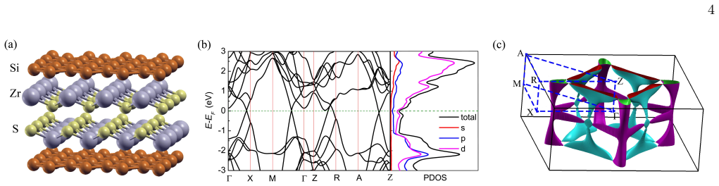
Measure the electron energy loss spectrum of a ZrSiS crystal under uniaxial strain: the paper predicts a sharp low-loss peak near 20 eV with anisotropic quadratic dispersion, and a separate check is that the in-plane and out-of-plane permittivities obtained from optical ellipsometry should have opposite signs in a ~0.6 eV window near 20 eV; if the 20 eV loss peak is absent or the permittivity signs are the same, the high-energy plasmon and hyperbolic claims fail. For the Lifshitz transition, quantum oscillation or ARPES measurements on a crystal under ~2 GPa tensile stress should show the hole pockets merging near $k_z=\pi/c$ and the quadratic band crossing the Fermi level along Z-R.
Extended reading notes
Core claim
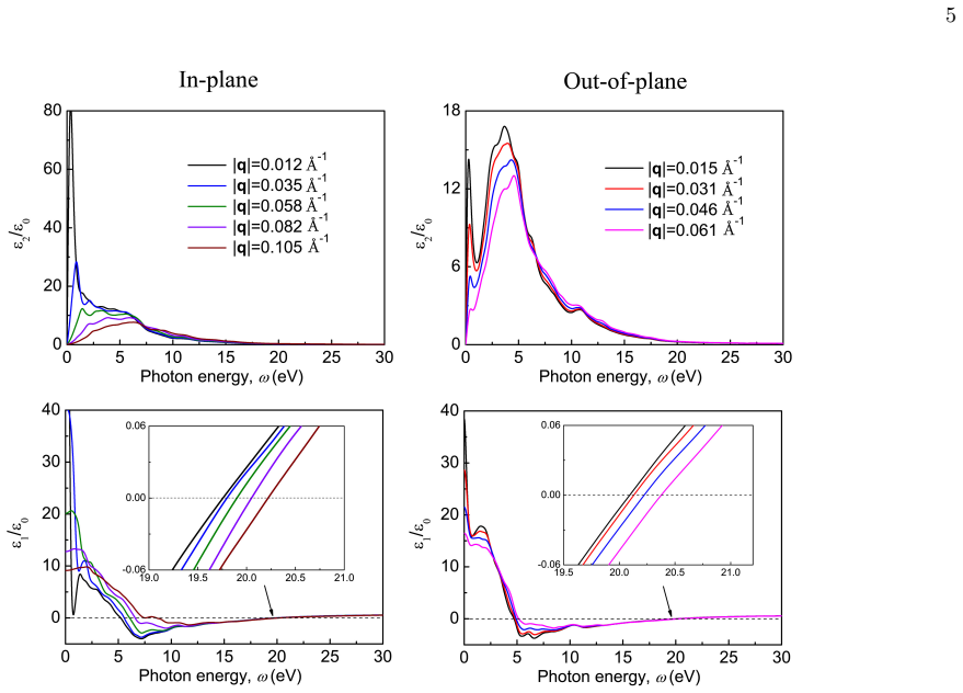
The central claim is that ZrSiS combines a strain-tolerant low-energy optical fingerprint with strain-tunable high-energy plasmonics. The frequency-independent in-plane optical conductivity, a known fingerprint of this nodal-line semimetal, remains flat under uniaxial compression up to 10 GPa, although the flat window shrinks and the spectral weight grows by roughly 50% at 5% compression. Tensile strain acts differently: near 1.3-3.4 GPa the Fermi surface changes topology through two Lifshitz transitions, and the resulting drop in interband screening reduces the infrared spectral weight and raises the screened plasma frequency from about 1.0 eV to about 1.3 eV at 4% tension. In the high-energy region, the calculations show a weakly damped plasmon near 20 eV whose quadratic dispersion is strongly anisotropic, and where the product of the in-plane and out-of-plane permittivities is negative over a ~0.6 eV window, the defining condition for type-I hyperbolic plasmons. The strain response of this high-energy mode is small in frequency but large in dispersion, so strain acts as a tuning knob rather than a switch.
Load-bearing premise
The load-bearing premise is that the calculated band structure and scalar dielectric function are accurate enough that the quadratic band sits at the right energy near the Fermi level and the permittivity signs near 20 eV are correct; a shift of a few tens of meV would move or erase the tensile Lifshitz transition, and wrong signs would make the hyperbolic regime an artifact of the calculation.
Editorial extensions
If this is right
- Uniaxial compression up to 10 GPa leaves the flat infrared conductivity intact, so ZrSiS-based infrared elements could tolerate large mechanical loads without losing their broadband response.
- Tensile stress near 2 GPa acts as a mechanical switch: the Lifshitz transition weakens interband screening and lowers the infrared spectral weight, with the effect saturating after the Fermi-surface reconstruction around 3.4 GPa.
- Electron energy loss measurements should find a sharp, low-loss peak near 20 eV whose dispersion is quadratic and markedly different in-plane and out-of-plane.
- The negative product of permittivities near 5 and 20 eV implies type-I hyperbolic plasmon propagation in windows of about 0.6 eV; the 20 eV window is the practically relevant one because the 5 eV mode is strongly damped.
- Strain of up to 5% changes the 20 eV plasmon frequency by only a few percent, but can change its out-of-plane dispersion coefficient by roughly 30%, giving a quantitative strain-tuning handle.
Reading between the lines
- Beyond the paper's own claims, the predicted tensile Lifshitz transition offers a clean test of the chemical-pressure picture: stretched ZrSiS should optically resemble ZrSiSe or ZrSiTe, and the ~2 GPa transition stress could be measured by quantum oscillations or ARPES under a four-point bending setup.
- Beyond the paper's own claims, the 20 eV hyperbolic window, if verified by EELS, would make ZrSiS one of the few natural (unstructured) hyperbolic materials in the deep ultraviolet; applications like subwavelength imaging and thermal emission engineering would follow without nanofabrication.
- Beyond the paper's own claims, since the scalar RPA neglects local-field effects and spin-orbit coupling, the most decisive numerical check is a full dielectric-matrix or Bethe-Salpeter calculation at 15-25 eV; if the sign of either permittivity changes there, the hyperbolic regime would move or disappear.
Signed reviews
Editorial analysis
A structured set of objections, weighed in public.
Referee Report
Summary. The manuscript reports first-principles calculations of the optical conductivity, dielectric function, and plasmonic response of the nodal-line semimetal ZrSiS, focusing on the effect of uniaxial strain. Using GGA-PBE band structures and a scalar RPA dielectric function with a Drude correction (Sec. II), the authors reproduce several low-energy experimental quantities for the pristine compound: the in-plane unscreened plasma frequency (3.15 vs 2.88 eV), the flat infrared conductivity (~7000 vs 6600 Ohm^-1 cm^-1), and epsilon_inf ~ 9 vs the experimental ~7.8. The main claims are that the frequency-independent infrared conductivity is robust under uniaxial compression up to 10 GPa but its flat region narrows with increasing compression; that tensile stress around 2 GPa induces a Lifshitz transition that weakens interband screening and reduces infrared spectral weight; and that the high-energy response hosts low-loss ~20 eV plasmons with strongly anisotropic dispersion, including a possible hyperbolic regime in the deep ultraviolet. The strain dependence of the high-energy plasmon dispersion is also discussed.
Significance. If the predictions hold, the paper identifies ZrSiS as a mechanically tunable natural hyperbolic material for ultraviolet plasmonics and connects the strain response to the chemical-pressure trend across the ZrSiX family (X=S, Se, Te). The manuscript has clear strengths: the zero-strain calculations are calibrated against measured optical quantities, the Drude contribution is handled explicitly, and the central predictions are concrete and falsifiable by EELS and infrared spectroscopy under uniaxial stress. The high-energy and tensile-strain predictions, however, rest on approximations that are not validated at the relevant energy scale, which is the main source of uncertainty in the paper.
major comments (3)
- [Abstract; Sec. IV, Fig. 8] The abstract and Conclusions state that 'Upon uniaxial tensile stress of 2 GPa, the Fermi surface undergoes a Lifshitz transition,' but Sec. IV identifies two Lifshitz transitions at P1 ≈ 1.3 GPa and P2 ≈ 3.4 GPa (with tension as negative stress in Fig. 8). The manuscript should reconcile this discrepancy: if the headline claim refers to the P1 transition, the abstract should say so and mention the second transition; if it refers to a single transition near 2 GPa, that conflicts with the two computed critical stresses. As written, the central quantitative claim is internally inconsistent.
- [Sec. IV, Figs. 7-8] The prediction that tensile strain of order 2 GPa triggers a Lifshitz transition and weakens interband screening depends on the energy position of the quadratic electron band along Z–R relative to the Fermi level. This band is obtained from GGA-PBE without spin-orbit coupling, and the calibration quantities in Sec. III A—unscreened plasma frequency, flat optical conductivity, and epsilon_inf—are aggregate low-energy properties that are insensitive to the band position at the meV scale. Because the stated SOC-induced gaps are up to ~20–30 meV, an error of that size could shift the critical strain substantially or remove the transition altogether. The authors should provide a direct check of this band's position (e.g., ARPES comparison, SOC-included band structure, or a hybrid-functional calculation) or explicitly qualify the predicted critical stress as an estimate with large uncertainty.
- [Sec. III B, Fig. 5] The claims of low-loss ~20 eV plasmons and a hyperbolic regime are based on the signs of epsilon_xx(omega) and epsilon_zz(omega) computed in the scalar RPA with local field effects neglected and using GGA-PBE band structures. The experimental calibration in Sec. III A covers only the low-energy (<= 2 eV) response; no independent check is presented for the ~20 eV region, where the permittivity signs are the load-bearing input for the hyperbolic dispersion. The authors should discuss the expected influence of local field effects, self-energy corrections, and SOC on the 20 eV permittivity, or compare with existing EELS or vacuum-UV optical data. Alternatively, the hyperbolic-regime claim should be explicitly labeled as a prediction that remains to be confirmed.
minor comments (5)
- [Sec. IV; Figs. 7 and 8] The strain sign convention is confusing: the text defines uzz as positive for compression and negative for tension, while the critical stresses are printed as P1 = -1.3 GPa and P2 = -3.4 GPa. Please adopt a single, clearly stated convention and apply it consistently in the text and figure captions.
- [Sec. II B, Eq. (8)] The expression for sigma_{2,intra}(omega) appears to be missing a factor of omega; the standard relation is sigma_2(omega) = omega [1 - epsilon_1(omega)]/(4 pi). Please check and correct the formula.
- [Sec. III B] There are several typographical errors in this section: 'Simliar' should be 'Similar', 'hyprobolic' should be 'hyperbolic' (twice), and 'electronmagnetic' should be 'electromagnetic'.
- [Sec. IV] In the discussion of the nonsymmorphic Dirac node, 'Andreas et al.' should be 'Topp et al.' (Ref. [13]) for accuracy.
- [Sec. IV, Eq. (10) and Fig. 10] The values of the dispersion coefficient A in Eq. (10) are not reported; given the paper's emphasis on strain tuning of the plasmon dispersion, providing A and its strain dependence would make the claim quantitative.
Circularity Check
No significant circularity: the central predictions are computed from first-principles DFT band structures and RPA response functions, with no target-derived fitting or load-bearing self-citation.
full rationale
The paper's central results — the flat infrared conductivity, its robustness and narrowing under compression, the tensile Lifshitz transition, the ~20 eV low-loss plasmons, and the hyperbolic UV regime — are all outputs of a DFT+RPA calculation, not quantities fed into the calculation. The only adjustable parameter is the damping η, which is set to 40 meV from the experimentally estimated electron linewidth (~30 meV at 300 K), and the resulting flat conductivity value (~7000 Ω−1cm−1) emerges from the computed band structure and matrix elements rather than being imposed by the choice of η. The Lifshitz transition at P1 ≈ 1.3 GPa and P2 ≈ 3.4 GPa is a band-structure consequence of the strain-dependent position of the quadratic electron band along Z–R relative to the Fermi level; no fitting to the claimed transition stress is performed. The high-energy plasmon and hyperbolic-regime claims follow directly from the momentum-resolved RPA dielectric function and the sign condition εxx(ω)·εzz(ω) < 0, with no parameter tuned to produce those signs. Comparisons to experiment (unscreened plasma frequency, flat conductivity, ε∞ ≈ 9 vs ~7.8) are validations rather than inputs. The chemical-pressure comparison to Ref. [45] is an independent external trend used for consistency, not a premise on which the strain calculations depend. Self-citations in Refs. [34,35,66] concern correlation effects or similar EELS behavior and are not load-bearing for the optical predictions. No uniqueness theorem, ansatz, or renamed empirical pattern is invoked as a substitute for computation. The paper therefore shows no circularity; any concern about GGA-PBE accuracy at the meV scale for the quadratic band is a correctness or robustness issue, not a circularity issue.
Assumptions & free parameters
free parameters (2)
- damping parameter eta =
40 meV
- Drude damping delta =
not stated
assumptions (4)
- domain assumption The independent-particle RPA with only the G=G'=0 head of the dielectric matrix is adequate; local field effects are negligible.
- domain assumption Spin-orbit coupling is negligible for the energy ranges considered (above 20 meV and above 100 K).
- domain assumption GGA-PBE exchange-correlation functional gives a quantitatively reliable band structure near the Fermi level and in the 0-20 eV range.
- domain assumption The intraband response can be described by a Drude term added separately to the interband RPA response.
Cite this review
Pith. "Pith review of Effect of mechanical strain on the optical properties of nodal-line semimetal ZrSiS." pith.science (2026). https://pith.science/paper/DPVFIEIP
@misc{pith2026190808789,
  author       = {Pith},
  title        = {Pith review of: Effect of mechanical strain on the optical properties of nodal-line semimetal ZrSiS},
  year         = {2026},
  howpublished = {\url{https://pith.science/paper/DPVFIEIP}},
  note         = {Machine review of arXiv:1908.08789}
}
abstract
Optical properties of nodal-line semimetal ZrSiS are studied using first-principles calculations. Frequency-independent optical conductivity is a fingerprint of the infrared optical response in ZrSiS. We find that this characteristic feature is robust with respect to uniaxial compressive strain of up to 10 GPa, yet with the flat region being narrowed with increasing strain. Upon uniaxial tensile stress of 2 GPa, the Fermi surface undergoes a Lifshitz transition accompanied by a weakening of the interband screening, which reduces the spectral weight of infrared excitations. We also show that the high-energy region is characterized by low-loss plasma excitations at $\sim$20 eV with essentially anisotropic dispersion. Strongly anisotropic dielectric properties suggest the existence of a hyperbolic regime for plasmons in the deep ultraviolet range. Although the frequencies of high-energy plasmons are virtually unaffected by external uniaxial deformation, their dispersion can be effectively tuned by strain.
Figures

Figures from the paper (6 more)


Reference graph
Works this paper leans on
-
[1]
The value obtained for the [100] directions is in good agreement with the exper- imental estimate of 2.88 eV [33]
components, respectively. The value obtained for the [100] directions is in good agreement with the exper- imental estimate of 2.88 eV [33]. In Figures 2(a) and 2(c), we show the real and imaginary parts of the optical conductivity calculated in the region up to 2 eV for [100] and [001] directions of photon propagation. The spectral weight obtained for th...
-
[2]
Young, S. M.; Zaheer, S.; Teo, J. C. Y.; Kane, C. L.; Mele, E. J.; Rappe, A. M. Phys. Rev. Lett. 2012, 108, 140405
work page 2012
-
[3]
Fisher, D. J. Topological Semimetals; Materials Research Forum LLC, 2019
work page 2019
-
[4]
Lv, B. Q.; Weng, H. M.; Fu, B. B.; Wang, X. P.; Miao, H.; Ma, J.; Richard, P.; Huang, X. C.; Zhao, L. X.; Chen, G. F.; Fang, Z.; Dai, X.; Qian, T.; Ding, H. Phys. Rev. X 2015, 5, 031013
work page 2015
-
[5]
Liu, Z.; Zhou, B.; Zhang, Y.; Wang, Z.; Weng, H.; Prab- hakaran, D.; Mo, S.-K.; Shen, Z.; Fang, Z.; Dai, X. Sci- ence 2014, 343, 864–867
work page 2014
- [6]
-
[7]
Xu, S.-Y.; Belopolski, I.; Alidoust, N.; Neupane, M.; Bian, G.; Zhang, C.; Sankar, R.; Chang, G.; Yuan, Z.; Lee, C.-C. Science 2015, 349, 613–617
work page 2015
-
[8]
Yu, R.; Weng, H.; Fang, Z.; Dai, X.; Hu, X. Phys. Rev. Lett. 2015, 115, 036807
work page 2015
Show all 81 references
-
[9]
A.; Hook, M
Burkov, A. A.; Hook, M. D.; Balents, L. Phys. Rev. B 2011, 84, 235126
2011
-
[10]
Okamoto, Y.; Inohara, T.; Yamakage, A.; Yamakawa, Y.; Takenaka, K. J. Phys. Soc. Jpn. 2016, 85, 123701
2016
-
[11]
Chen, Y.; Lu, Y.-M.; Kee, H.-Y. Nat. Commun. 2015, 6, 6593
2015
-
[12]
M.; Ali, M
Schoop, L. M.; Ali, M. N.; Straßer, C.; Topp, A.; Varykhalov, A.; Marchenko, D.; Duppel, V.; Parkin, S. S.; Lotsch, B. V.; Ast, C. R. Nat. Com- mun. 2016, 7, 11696
2016
-
[13]
Bian, G.; Chang, T.-R.; Sankar, R.; Xu, S.-Y.; Zheng, H.; Neupert, T.; Chiu, C.-K.; Huang, S.-M.; Chang, G.; Be- lopolski, I. Nat. Commun. 2016, 7, 10556
2016
-
[14]
Emmanouilidou, E.; Shen, B.; Deng, X.; Chang, T.-R.; Shi, A.; Kotliar, G.; Xu, S.-Y.; Ni, N.Phys. Rev. B 2017, 95, 245113
2017
-
[15]
M.; Varykhalov, A.; Duppel, V.; Lotsch, B
Topp, A.; Lippmann, J. M.; Varykhalov, A.; Duppel, V.; Lotsch, B. V.; Ast, C. R.; Schoop, L. M. New J. Phys. 2016, 18, 125014
2016
-
[16]
N.; Wei, J.; Mao, Z
Hu, J.; Tang, Z.; Liu, J.; Liu, X.; Zhu, Y.; Graf, D.; Myhro, K.; Tran, S.; Lau, C. N.; Wei, J.; Mao, Z. Phys. Rev. Lett. 2016, 117, 016602
2016
-
[17]
Matusiak, M.; Cooper, J.; Kaczorowski, D. Nat. Com- mun. 2017, 8, 15219
2017
-
[18]
M.; Dimitri, K.; Belopolski, I.; Maldonado, P.; Sankar, R.; Dhakal, N.; Dhakal, G.; Cole, T.; Oppe- neer, P
Hosen, M. M.; Dimitri, K.; Belopolski, I.; Maldonado, P.; Sankar, R.; Dhakal, N.; Dhakal, G.; Cole, T.; Oppe- neer, P. M.; Kaczorowski, D.; Chou, F.; Hasan, M. Z.; Durakiewicz, T.; Neupane, M. Phys. Rev. B 2017, 95, 161101
2017
-
[19]
J.; Cao, C.; Fogler, M
Shao, Y.; Sun, Z.; Wang, Y.; Xu, C.; Sankar, R.; Brein- del, A. J.; Cao, C.; Fogler, M. M.; Millis, A. J.; Chou, F.; Li, Z.; Timusk, T.; Maple, M. B.; Basov, D. N. Proc. Natl. Acad. Sci. U.S.A. 2019, 116, 1168
2019
-
[20]
Chen, C. et al. Phys. Rev. B 2017, 95, 125126
2017
-
[21]
W.; Varykhalov, A.; Marchenko, D.; Krivenkov, M.; Rodolakis, F.; McChesney, J
Topp, A.; Queiroz, R.; Gr¨ uneis, A.; M¨ uchler, L.; Rost, A. W.; Varykhalov, A.; Marchenko, D.; Krivenkov, M.; Rodolakis, F.; McChesney, J. L.; Lotsch, B. V.; Schoop, L. M.; Ast, C. R. Phys. Rev. X 2017, 7, 041073
2017
-
[22]
J.; Wu, Y.-M.; Hsing, C.-R.; Tseng, Y.; Sankar, R.; Wei, C.-M.; Chou, F.-C.; Lin, M.-T
Butler, C. J.; Wu, Y.-M.; Hsing, C.-R.; Tseng, Y.; Sankar, R.; Wei, C.-M.; Chou, F.-C.; Lin, M.-T. Phys. Rev. B 2017, 96, 195125. 11
2017
-
[23]
arXiv preprint arXiv:1712.00782 2017,
Fu, B.; Yi, C.; Zhang, T.; Caputo, M.; Ma, J.; Gao, X.; Lv, B.; Kong, L.; Huang, Y.; Shi, M. arXiv preprint arXiv:1712.00782 2017,
2017 arXiv
-
[24]
Pezzini, S.; Van Delft, M.; Schoop, L.; Lotsch, B.; Car- rington, A.; Katsnelson, M.; Hussey, N.; Wiedmann, S. Nat. Phys. 2018, 14, 178
2018
-
[25]
S.; Chang, G.; Huang, C.-Y.; Singh, B.; Hellerstedt, J.; Edmonds, M
Lodge, M. S.; Chang, G.; Huang, C.-Y.; Singh, B.; Hellerstedt, J.; Edmonds, M. T.; Kaczorowski, D.; Ho- sen, M. M.; Neupane, M.; Lin, H. Nano Lett. 2017, 17, 7213–7217
2017
-
[26]
Wang, X.; Pan, X.; Gao, M.; Yu, J.; Jiang, J.; Zhang, J.; Zuo, H.; Zhang, M.; Wei, Z.; Niu, W. Adv. Electron. Mater 2016, 2, 1600228
2016
-
[27]
Hu, J.; Tang, Z.; Liu, J.; Zhu, Y.; Wei, J.; Mao, Z. Phys. Rev. B 2017, 96, 045127
2017
-
[28]
N.; Schoop, L
Ali, M. N.; Schoop, L. M.; Garg, C.; Lippmann, J. M.; Lara, E.; Lotsch, B.; Parkin, S. S. Sci. Adv. 2016, 2, e1601742
2016
-
[29]
K.; Satpati, B.; Mandal, P
Singha, R.; Pariari, A. K.; Satpati, B.; Mandal, P. Proc. Natl. Acad. Sci. 2017, 114, 2468–2473
2017
-
[30]
P.; But- ler, C
Sankar, R.; Peramaiyan, G.; Muthuselvam, I. P.; But- ler, C. J.; Dimitri, K.; Neupane, M.; Rao, G. N.; Lin, M.- T.; Chou, F. Sci. Rep. 2017, 7, 40603
2017
-
[31]
Pan, H.; Tong, B.; Yu, J.; Wang, J.; Fu, D.; Zhang, S.; Wu, B.; Wan, X.; Zhang, C.; Wang, X. Sci. Rep. 2018, 8, 9340
2018
-
[32]
M.; Sanchez, D
Neupane, M.; Belopolski, I.; Hosen, M. M.; Sanchez, D. S.; Sankar, R.; Szlawska, M.; Xu, S.- Y.; Dimitri, K.; Dhakal, N.; Maldonado, P.; Oppe- neer, P. M.; Kaczorowski, D.; Chou, F.; Hasan, M. Z.; Durakiewicz, T. Phys. Rev. B 2016, 93, 201104
2016
-
[33]
Lam, R.; Mar, A. J. Solid State Chem. 1997, 134, 388– 394
1997
-
[34]
N.; Stepanov, E
Rudenko, A. N.; Stepanov, E. A.; Lichtenstein, A. I.; Katsnelson, M. I. Phys. Rev. Lett. 2018, 120, 216401
2018
-
[35]
B.; Schoop, L
Schilling, M. B.; Schoop, L. M.; Lotsch, B. V.; Dres- sel, M.; Pronin, A. V.Phys. Rev. Lett. 2017, 119, 187401
2017
-
[36]
A.; Yerger, C
VanGennep, D.; Paul, T. A.; Yerger, C. W.; Weir, S. T.; Vohra, Y. K.; Hamlin, J. J. Phys. Rev. B 2019, 99, 085204
2019
-
[37]
M.; Honerkamp, C.; Rudenko, A
Scherer, M. M.; Honerkamp, C.; Rudenko, A. N.; Stepanov, E. A.; Lichtenstein, A. I.; Katsnelson, M. I. Phys. Rev. B 2018, 98, 241112
2018
-
[38]
arXiv preprint arXiv:1904.05628 2019,
Wang, J.; Sui, X.; Gao, S.; Duan, W.; Liu, F.; Huang, B. arXiv preprint arXiv:1904.05628 2019,
1904 arXiv
-
[39]
B.; van Heumen, E.; Carbone, F.; van der Marel, D
Kuzmenko, A. B.; van Heumen, E.; Carbone, F.; van der Marel, D. Phys. Rev. Lett. 2008, 100, 117401
2008
-
[40]
F.; Sfeir, M
Mak, K. F.; Sfeir, M. Y.; Wu, Y.; Lui, C. H.; Mis- ewich, J. A.; Heinz, T. F. Phys. Rev. Lett. 2008, 101, 196405
2008
-
[41]
B´ acsi, A.; Virosztek, A.Phys. Rev. B 2013, 87, 125425
2013
-
[42]
M.; Zhao, L
Xu, B.; Dai, Y. M.; Zhao, L. X.; Wang, K.; Yang, R.; Zhang, W.; Liu, J. Y.; Xiao, H.; Chen, G. F.; Tay- lor, A. J.; Yarotski, D. A.; Prasankumar, R. P.; Qiu, X. G. Phys. Rev. B 2016, 93, 121110
2016
-
[43]
Y.; Zhang, S
Chen, R. Y.; Zhang, S. J.; Schneeloch, J. A.; Zhang, C.; Li, Q.; Gu, G. D.; Wang, N. L. Phys. Rev. B 2015, 92, 075107
2015
-
[44]
Habe, T.; Koshino, M. Phys. Rev. B 2018, 98, 125201
2018
-
[45]
P.; Nateprov, A
Neubauer, D.; Carbotte, J. P.; Nateprov, A. A.; L¨ ohle, A.; Dressel, M.; Pronin, A. V.Phys. Rev. B 2016, 93, 121202
2016
-
[46]
Lv, Y.-Y.; Zhang, B.-B.; Li, X.; Yao, S.-H.; Chen, Y.; Zhou, J.; Zhang, S.-T.; Lu, M.-H.; Chen, Y.-F. Appl. Phys. Lett. 2016, 108, 244101
2016
-
[47]
F.; Krottenm¨ uller, M.; Hu, J.; Zhu, Y
Ebad-Allah, J.; Afonso, J. F.; Krottenm¨ uller, M.; Hu, J.; Zhu, Y. L.; Mao, Z. Q.; Kuneˇ s, J.; Kuntscher, C. A.Phys. Rev. B 2019, 99, 125154
2019
-
[48]
M.; Schatz, G
McMahon, J. M.; Schatz, G. C.; Gray, S. K. Phys. Chem. Chem. Phys. 2013, 15, 5415–5423
2013
-
[49]
Politano, A.; Chiarello, G. Progr. Surf. Sci 2015, 90, 144–193
2015
-
[50]
C.; Ponraj, J
Dhanabalan, S. C.; Ponraj, J. S.; Zhang, H.; Bao, Q. Nanoscale 2016, 8, 6410–6434
2016
-
[51]
Taguchi, A.; Saito, Y.; Watanabe, K.; Yijian, S.; Kawata, S. Appl. Phys. Lett. 2012, 101, 081110
2012
-
[52]
Nakashima, S.-I.; Okumura, H.; Yamamoto, T.; Shimidzu, R. Appl. Spectrosc. 2004, 58, 224–229
2004
-
[53]
IEEE Photonics Technol
Zhang, X.; Wang, K.; Ma, J.; Zhang, Q.; Yan, P.; Tian, X. IEEE Photonics Technol. Lett. 2015, 27, 1297– 1300
2015
-
[54]
B.; Calandra, M.; Car, R.; Cavazzoni, C.; Ceresoli, D.; Cococcioni, M
Giannozzi, P.; Andreussi, O.; Brumme, T.; Bunau, O.; Nardelli, M. B.; Calandra, M.; Car, R.; Cavazzoni, C.; Ceresoli, D.; Cococcioni, M. J. Phys. Condens. Matter 2017, 29, 465901
2017
-
[55]
K.; Zillohu, A.; Strunskus, T.; Faupel, F.; Elbahri, M
Hedayati, M. K.; Zillohu, A.; Strunskus, T.; Faupel, F.; Elbahri, M. Appl. Phys. Lett. 2014, 104, 041103
2014
-
[56]
R.; Schl¨ uter, M.; Chiang, C.Phys
Hamann, D. R.; Schl¨ uter, M.; Chiang, C.Phys. Rev. Lett. 1979, 43, 1494–1497
1979
-
[57]
P.; Burke, K.; Ernzerhof, M
Perdew, J. P.; Burke, K.; Ernzerhof, M. Phys. Rev. Lett. 1996, 77, 3865–3868
1996
-
[58]
Marini, A.; Hogan, C.; Gr¨ uning, M.; Varsano, D.Comp. Phys. Commun. 2009, 180, 1392–1403
2009
-
[59]
Kokalj, A. Comp. Mater. Sci. 2003, 28, 155–168
2003
-
[60]
Marder, M. P. Condensed Matter Physics , 2nd ed.; John Wiley & Sons, Hoboken, New Jersey, 2010
2010
-
[61]
Onida, G.; Reining, L.; Rubio, A. Rev. Mod. Phys. 2002, 74, 601–659
2002
-
[62]
Dressel, M.; Gr¨ uner, G.Electrodynamics of Solids; Cam- bridge University Press, U.K., 2002
2002
-
[63]
Sangalli, D.; Ferretti, A.; Miranda, H.; Attaccalite, C.; Marri, I.; Cannuccia, E.; Melo, P.; Marsili, M.; Paleari, F.; Marrazzo, A. J. Phys.: Cond. Matter 2019, 31, 325902
2019
-
[64]
D.; Hohage, M.; Zeppen- feld, P
Harl, J.; Kresse, G.; Sun, L. D.; Hohage, M.; Zeppen- feld, P. Phys. Rev. B 2007, 76, 035436
2007
-
[65]
Lee, K.-H.; Chang, K. J. Phys. Rev. B 1994, 49, 2362– 2367
1994
-
[66]
Nanoscale 2018, 10, 21918–21927
Nicotra, G.; van Veen, E.; Deretzis, I.; Wang, L.; Hu, J.; Mao, Z.; Fabio, V.; Spinella, C.; Chiarello, G.; Rudenko, A. Nanoscale 2018, 10, 21918–21927
2018
-
[67]
Prandini, G.; Galante, M.; Marzari, N.; Umari, P. Comp. Phys. Commun. 2019,
2019
-
[68]
2014, 1, 14
Shekhar, P.; Atkinson, J.; Jacob, Z.Nano Converg. 2014, 1, 14
2014
-
[69]
Sensors 2013, 13, 10482– 10518
Sang, L.; Liao, M.; Sumiya, M. Sensors 2013, 13, 10482– 10518
2013
-
[70]
N.; Petersen, R.; Pedersen, T
Gjerding, M. N.; Petersen, R.; Pedersen, T. G.; Mortensen, N. A.; Thygesen, K. S. Nat. Commun. 2017, 8, 320
2017
-
[71]
S.; Tymchenko, M.; Al` u, A
Gomez-Diaz, J. S.; Tymchenko, M.; Al` u, A. Phys. Rev. Lett. 2015, 114, 233901
2015
-
[72]
M.; Zhang, X
Yao, J.; Liu, Z.; Liu, Y.; Wang, Y.; Sun, C.; Bartal, G.; Stacy, A. M.; Zhang, X. Science 2008, 321, 930–930
2008
-
[73]
L.; Jacob, Z
Guo, Y.; Newman, W.; Cortes, C. L.; Jacob, Z. Adv. Optoelectron. 2012, 2012, 452502
2012
-
[74]
V.; Ginzburg, P.; Rodr´ ıguez- Fortu˜ no, F
Kapitanova, P. V.; Ginzburg, P.; Rodr´ ıguez- Fortu˜ no, F. J.; Filonov, D. S.; Voroshilov, P. M.; Belov, P. A.; Poddubny, A. N.; Kivshar, Y. S.; 12 Wurtz, G. A.; Zayats, A. V. Nat. Commun. 2014, 5, 3226
2014
-
[75]
J.; Alekseyev, L.; Howard, S
Hoffman, A. J.; Alekseyev, L.; Howard, S. S.; Franz, K. J.; Wasserman, D.; Podolskiy, V. A.; Nari- manov, E. E.; Sivco, D. L.; Gmachl, C.Nat. Mater. 2007, 6, 946
2007
-
[76]
L.; Mao, Z
Ebad-Allah, J.; Krottenm¨ uller, M.; Hu, J.; Zhu, Y. L.; Mao, Z. Q.; Kuntscher, C. A. Phys. Rev. B 2019, 99, 245133
2019
-
[77]
Biehs, S.-A.; Tschikin, M.; Ben-Abdallah, P. Phys. Rev. Lett. 2012, 109, 104301
2012
-
[78]
Salmankurt, B.; Duman, S. Philos. Mag. 2017, 97, 175– 186
2017
-
[79]
D.; Lifshitz, E
Landau, L. D.; Lifshitz, E. M. Course of Theoretical Physics, Vol.7: Elasticity theory , 3rd ed.; Pergamon Press, Oxford, U.K., 1989
1989
-
[81]
IEEE Electron Device Lett
Suthram, S.; Ziegert, J.; Nishida, T.; Thompson, S. IEEE Electron Device Lett. 2006, 28, 58–61
2006
-
[100]
can clearly see the prominent flat conductivity from 0.1 to 0.4 eV
and out-of-plane [001] crystallographic directions; (b) Real part of the in-plane optical conductivity calculated for different damping parametersη; (c) Imaginary part of the op- tical conductivity calculated along [100] and [001] directions; (d) Real part of the in-plane diele...
Reviewed August 14, 2026 · model on record in the stance chip above.
Discussion (0). Continue with ORCID to comment.