REVIEW 4 major objections 5 minor 61 references
Graphene/hBN heterostructure based Valley transistor: Dynamic Control of valley current in synchronized nonzero voltages, within the time-dependent regime
T0 review · 4 major / 5 minor · reviewed 2026-08-07 · deepseek-v4-flash
Pith's one-line read This paper claims that synchronizing the tip and bias gates with the same polarity in a graphene/hBN device produces a periodically alternating, pure valley-polarized current, and that reversing the common polarity swaps which valley is ON.
desk verdict A genuine dual-gate valley-switching protocol shown in a tight-binding model, resting on an assumed Gaussian tip potential; the paper overclaims self-consistency and time-dependence. read the letter →
The pith
A machine-rendered reading of the paper's core claim, the machinery that carries it, and where it could break.
The reading
What carries the argument
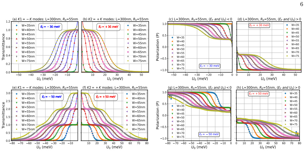
The load-bearing object is the sign-controlled Gaussian tip-gate potential $U(r,t)=U_0(t)\exp(-r^2/R_0^2)$, added to a nearest-neighbor tight-binding Hamiltonian of graphene that also includes a small staggered sublattice potential ($\Delta_{SG}\approx 29$ meV). Its sign relative to the Fermi level determines whether electrons or holes are trapped in the hBN spacer, which breaks electron-hole symmetry and sends the two valleys into different scattering outcomes. The argument is carried by the valley-resolved transmission $T_{\pm K}(E)$ computed within the non-equilibrium Green's function formalism, the polarization $P=(T_{-K}-T_{+K})/(T_{-K}+T_{+K})$, and the periodic square-wave driving of both gates at matched frequency and polarity, which produces the complementary ON/OFF currents in the time domain.
What would settle it
Run the same two-terminal transport calculation with a self-consistently screened potential (solving Poisson's equation for the tip, hBN spacer, and graphene charge) instead of the fixed Gaussian $U(r)$; if the fully polarized alternating ON/OFF valley currents disappear, the central claim fails. Alternatively, a real device driven with synchronized same-polarity square pulses should show $I_{-K}$ ON while $I_{+K}$ is OFF in one half-cycle and the exact swap in the other—any simultaneous conduction of both valleys would refute it.
Extended reading notes
Core claim
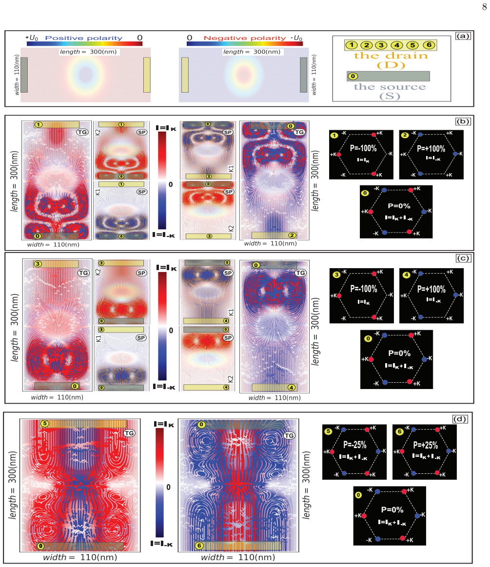
The central claim is that synchronized same-polarity gate pulses turn the graphene/hBN heterostructure into a valley field-effect transistor that works at nonzero bias. In the time-dependent regime, the authors compute valley-resolved currents $I_{-K}$ and $I_{+K}$ from a tight-binding Hamiltonian with a Gaussian tip-induced potential $U(r)=U_0\exp(-r^2/R_0^2)$ and a time-varying sample bias. When both gates carry a square wave with the same sign, the channel transmits only one valley at a time: for positive gates the $+K$ current is ON and the $-K$ current is OFF in the forward half-cycle, and in the reversed half-cycle the $-K$ current is ON and the $+K$ current is OFF. Reversing the common polarity swaps which valley is transmitted, and the same-polarity condition ($V_B\,U_0 > 0$) is the regime where the valley polarization $P=(T_{-K}-T_{+K})/(T_{-K}+T_{+K})$ reaches $\pm1$. Opposite gate polarities leave both valleys partially transmitting ($P \approx \pm25\%$) and do not give valve behavior.
Load-bearing premise
The whole effect relies on the KPFM tip imprinting a fixed Gaussian potential $U(r)=U_0\exp(-r^2/R_0^2)$ on the graphene with a sign that directly selects electron versus hole trapping in the hBN; if the real screened potential differs in shape or does not break electron-hole symmetry in that way, the predicted valley switching would not occur.
Editorial extensions
If this is right
- A graphene/hBN device can switch valley currents at finite bias using only gate voltages of a few meV, suggesting low-power valleytronic logic.
- The complementary nature of $I_{-K}$ and $I_{+K}$ means the same device outputs both a forward and a reverse valley current, selectable by the common sign of the two gates.
- The ON/OFF states follow the square-wave period, so the same setup acts as a time-modulated valley current source rather than a static filter.
- The condition $V_B \times U_0 > 0$ (same polarity) is the operative design rule; opposite polarity yields only partial polarization and no clean valley switch.
- Sample width and potential radius $R_0$ set the usable bias range, so the valley transistor's operating window can be tuned geometrically.
Reading between the lines
- Editorial inference: the same polarity-matching mechanism could in principle be transferred to other two-dimensional semiconductors with broken sublattice symmetry, where a local gate rather than strain selects the valley.
- Editorial inference: because the paper assumes the pulse period is long enough for steady state, a natural test would be to sweep the gate frequency upward and map where the ON/OFF valley contrast degrades—this would define the switching bandwidth of the proposed transistor.
- Editorial inference: the fixed Gaussian potential is an approximation; a self-consistent Poisson calculation that includes charge redistribution in the hBN spacer would indicate whether the effect survives realistic screening and would revise the required bias ranges.
- Editorial inference: the complementary $K$/$K'$ currents could serve as a differential pair, so reading the difference $I_{-K} - I_{+K}$ would suppress common-mode noise in a valley-based circuit.
Editorial analysis
A structured set of objections, weighed in public.
Referee Report
Summary. The paper proposes a graphene/hBN metal-insulator-semiconductor device in which a KPFM tip gate and a sample bias gate are driven by synchronized square voltages. Using a tight-binding Hamiltonian with a staggered sublattice potential and a Gaussian tip-induced potential, the authors compute valley-resolved transmission with Kwant/NEGF and identify parameter regimes where the two valley currents (I_{K1=-K} and I_{K2=+K}) are alternately ON and OFF, yielding complementary valley-switching behavior even at finite bias. The central claim is that same-polarity synchronized gates produce a periodically modulated pure valley-polarized current, with opposite valley selectivity when the gate polarity is reversed.
Significance. If the result holds, the paper offers a conceptually simple and potentially low-power route to a valley transistor based on electrostatic gating rather than strain or magnetic fields. The numerical work is reproducible in principle: the Hamiltonian is explicitly stated, the Kwant/NEGF method is standard, and the ON/OFF complementarity in Fig. 5 is visually clear. The main weakness is that the valley-selection mechanism rests on an assumed Gaussian potential whose sign and shape are not derived from any self-consistent electrostatics, and the manuscript contains several internal inconsistencies about the polarity and magnitude conditions required for pure valley currents. The idea is worth pursuing, but the central claim, as stated, is not yet established.
major comments (4)
- [Sec. II, Eq. (2)] The paper states that the total screened potential U(r_i,t)=U0(t) exp(-r_i^2/R0^2) is "resolved self-consistently and experimentally," but no self-consistent Poisson or screening calculation and no experimental potential map are presented. Because the sign and spatial form of this Gaussian potential are the only physical mechanism that selects the valley and the electron/hole trapping asymmetry, the central ON/OFF valley-switching result in Sec. III.B.2 is conditional on this assumption. Please either provide a self-consistent electrostatic calculation for the KPFM/hBN/graphene stack, or explicitly present Eq. (2) as a model assumption and discuss how deviations from this form would affect the predicted switching.
- [Sec. III.B.1] The three stated conditions for pure valley current at the end of Sec. III.B.1 include |VB| > |U0| and zero bias in the second half of the modulation, yet Fig. 5 presents pure valley currents for |U0| > |VB| with both gates nonzero and synchronized. Moreover, Fig. 3(b),(f), which satisfy |VB| > |U0|, show unpolarized conduction rather than a pure valley current. The selection rule for the synchronized-gate regime therefore needs to be stated separately and consistently; as written, the text is internally contradictory.
- [Sec. II and Sec. III.B] The manuscript describes a "time-dependent regime" and "dynamic control," but all currents are computed from the stationary Landauer-type formula Eq. (3) using the instantaneous DC transmission at each voltage step, under the assumption that the signal period is longer than any characteristic time. This quasi-static/adiabatic reduction is not demonstrated for the parameters used. Please provide the relevant time scales (e.g., charging time, transit time, RC time) and a quantitative adiabaticity criterion; otherwise the time-dependent claim is not established.
- [Sec. II] Section II states that the sample bias is "mainly set to be opposit to that of the tip gate electrode (VB × VT < 0)", while the central result in Sec. III.B.2 requires the tip and bias gates to have the same polarity during synchronized operation. This direct contradiction in the setup should be resolved; the text should state clearly which polarity configuration is used for the transistor mode.
minor comments (5)
- [Sec. III, opening paragraph] The text sets the Gaussian radius to R0 = 35 nm, but all figures use R0 = 55 nm; please harmonize the stated value with the numerical simulations.
- [Figs. 3 and 5] The current axis labels are garbled ("I( A)" and "I( /uni03BCμ )"); please specify the units, presumably µA, clearly on all panels.
- [Fig. 4 caption] The caption states "VB=±30 meV (top panels) and VB=±30 meV (bottom panels)"; the bottom panels should be ±50 meV according to the text and panel annotations.
- [Appendix C, Eq. (C.1)] The sentence "the hopping matrices in the heterostructure are obtained from the first term of Eq. 2" should refer to Eq. (1), since Eq. (2) is the Gaussian potential, not the Hamiltonian.
- [Throughout] There are several typographical errors (e.g., "opposit" in Sec. II, "EE=VB" in Sec. III.B.1, "teh" in the conclusion, "Fortunetaly" in Sec. II) that should be corrected in a revision.
Circularity Check
No significant circularity: the valley-switching results are numerical outputs of the assumed tight-binding Hamiltonian, with gate voltages as scanned control parameters; remaining self-citation is not load-bearing.
full rationale
The central derivation is self-contained as a transport calculation. Starting from the tight-binding Hamiltonian in Eq. (1) with the Gaussian potential in Eq. (2), the paper computes valley-resolved currents via NEGF/Kwant (Eq. (3) and Appendix A). U0 and VB are scanned control parameters, not fitted to the target ON/OFF pattern, so the switching displayed in Figs. 3-6 is a numerical output rather than a fitted input renamed as a prediction. The only self-referential element is the citation [58] (Nedell et al., including co-author A. Abbout) used to justify discarding intervalley mixing; this is not load-bearing because the paper's own computed P = ±1 polarization maps independently demonstrate that, in the regimes considered, valley mixing is low. The Gaussian form of U(r) is an assumption rather than a self-consistently solved potential, and the successful synchronized cases in Fig. 5 use |U0| > |VB| despite the Sec. III.B.1 statement that |VB| > |U0| is required; these are correctness/consistency concerns, not circularity. No prediction reduces by construction to an input parameter or to an unverified self-citation.
Assumptions & free parameters
free parameters (6)
- U0 (tip-induced potential amplitude) =
±25, ±50, ±75 meV
- VB (sample bias amplitude) =
±30, ±50 meV
- R0 (Gaussian potential radius) =
35 nm (Sec. III) or 55 nm (Sec. II and captions)
- W (ribbon width) =
70 nm and 110 nm
- L (ribbon length) =
300 nm
- T (square-wave period) =
20 s
assumptions (5)
- ad hoc to paper A localized electrostatic potential in graphene can be represented by a smooth Gaussian U(r)=U0 exp(-r^2/R0^2) whose sign selects electron or hole trapping.
- domain assumption The graphene/hBN band structure is captured by a nearest-neighbor tight-binding Hamiltonian with a constant staggered sublattice potential Delta_SG=29.26 meV.
- domain assumption Intervalley scattering is weak enough that pure valley currents can be defined and valley mixing discarded.
- domain assumption The square-wave period is long enough for the device to reach steady state within each half-period, so time-dependent response equals DC valley-resolved conductance.
- standard math Lead self-energies are treated in the wide-band limit.
Cite this review
Pith. "Pith review of Graphene/hBN heterostructure based Valley transistor: Dynamic Control of valley current in synchronized nonzero voltages, within the time-dependent regime." pith.science (2026). https://pith.science/paper/ED22ZUEM
@misc{pith2026250521295,
  author       = {Pith},
  title        = {Pith review of: Graphene/hBN heterostructure based Valley transistor: Dynamic Control of valley current in synchronized nonzero voltages, within the time-dependent regime},
  year         = {2026},
  howpublished = {\url{https://pith.science/paper/ED22ZUEM}},
  note         = {Machine review of arXiv:2505.21295}
}
read the original abstract
Graphene/hexagonal boron nitride (hBN) heterostructures represent a promising class of metal-insulator-semiconductor systems widely explored for multifunctional digital device applications. In this work, we demonstrate that graphene, when influenced by carrier-dependent trapping in the hBN spacer triggered by a localized potential from Kelvin probe force microscopy (KPFM), can exhibit valley transistor behavior under specific conditions. We employ a tight-binding model that self-consistently incorporates a Gaussian-shaped potential to represent the effect of the tip gate. Crucially, we show that the heterostructure functions as a field-effect transistor (FET), with its operation governed by the bias gate (shifting the Fermi level) and the tip-induced potential (breaking electron-hole symmetry via selective trapping of electron or hole quasiparticles). Our results reveal that, under specific lattice geometry, pulse frequency, and gate voltage conditions, the device exhibits valley transistor functionality. The valley current (e.g., I_K1=-K or I_K2=+K) can be selectively controlled by synchronizing the frequencies and polarities of the tip and bias gate voltages. Notably, when both gates are driven with the same polarity, the graphene channel outputs a periodically modulated, pure valley-polarized current. This enables switching between distinct ON/OFF valley current states even at finite bias. Remarkably, when the I_K1=-K current is ON (forward current), the I_K2=+K current is OFF. Reversing the gate polarity inverts this behavior: I_K1=-K turns OFF, while I_K2=+K turns ON (reverse current). These findings pave the way toward low-voltage valley transistors in metal-insulator-semiconductor architectures, offering new avenues for valleytronics and advanced gating technologies.
Figures


Figures from the paper (3 more)

Reference graph
Works this paper leans on
-
[1]
author A. K. Geim and author K. S. Novoselov , journal Nature materials volume 6 , pages 183 ( year 2007 )
work page 2007
-
[2]
author A. Curtin , author M. Fuhrer , author J. Tedesco , author R. Myers-Ward , author C. Eddy , and author D. Gaskill , journal Applied Physics Letters volume 98 ( year 2011 )
work page 2011
-
[3]
author T. Frank , author S. Irmer , author M. Gmitra , author D. Kochan , and author J. Fabian , journal Physical Review B volume 95 , pages 035402 ( year 2017 )
work page 2017
-
[4]
author Z. Fan , author J. H. Garcia , author A. W. Cummings , author J. E. Barrios-Vargas , author M. Panhans , author A. Harju , author F. Ortmann , and author S. Roche , journal Physics Reports volume 903 , pages 1 ( year 2021 )
work page 2021
-
[5]
author J. F. Sierra , author J. Fabian , author R. K. Kawakami , author S. Roche , and author S. O. Valenzuela , journal Nature Nanotechnology volume 16 , pages 856 ( year 2021 )
work page 2021
-
[6]
author K. Zollner , author A. W. Cummings , author S. Roche , and author J. Fabian , journal Physical Review B volume 103 , pages 075129 ( year 2021 )
work page 2021
-
[7]
author T. Naimer , author K. Zollner , author M. Gmitra , and author J. Fabian , journal Physical Review B volume 104 , pages 195156 ( year 2021 )
work page 2021
-
[8]
author A. Belayadi and author P. Vasilopoulos , journal Nanotechnology volume 34 , pages 365706 ( year 2023 )
work page 2023
Show all 61 references
-
[9]
Milovanovi \'c and author F
author S. Milovanovi \'c and author F. Peeters , journal Applied Physics Letters volume 109 ( year 2016 )
2016
-
[10]
Rycerz , author J
author A. Rycerz , author J. Tworzyd o , and author C. Beenakker , journal Nature Physics volume 3 , pages 172 ( year 2007 )
2007
-
[11]
author V. M. Pereira and author A. Castro Neto , journal Physical review letters volume 103 , pages 046801 ( year 2009 )
2009
-
[12]
Vozmediano , author M
author M. Vozmediano , author M. Katsnelson , and author F. Guinea , journal Physics Reports volume 496 , pages 109 ( year 2010 ), ISSN issn 0370-1573 , ://www.sciencedirect.com/science/article/pii/S0370157310001729
2010
-
[13]
Settnes , author S
author M. Settnes , author S. R. Power , author M. Brandbyge , and author A.-P. Jauho , journal Physical review letters volume 117 , pages 276801 ( year 2016 )
2016
-
[14]
Kumari , author G
author R. Kumari , author G. Dixit , and author A. Kundu , journal Phys. Rev. B volume 111 , pages 155421 ( year 2025 ), ://link.aps.org/doi/10.1103/PhysRevB.111.155421
2025 doi
-
[15]
Da Costa , author A
author D. Da Costa , author A. Chaves , author S. Sena , author G. Farias , and author F. Peeters , journal Physical Review B volume 92 , pages 045417 ( year 2015 )
2015
-
[16]
Tao and author E
author L. Tao and author E. Y. Tsymbal , journal Physical Review B volume 100 , pages 161110 ( year 2019 )
2019
-
[17]
Liu , author Z
author Y.-W. Liu , author Z. Hou , author S.-Y. Li , author Q.-F. Sun , and author L. He , journal Physical review letters volume 124 , pages 166801 ( year 2020 a )
2020
-
[18]
Zambrano , author P
author D. Zambrano , author P. Orellana , author L. Rosales , and author A. Latg \'e , journal Physical Review Applied volume 15 , pages 034069 ( year 2021 )
2021
-
[19]
Aktor , author J
author T. Aktor , author J. H. Garcia , author S. Roche , author A.-P. Jauho , and author S. R. Power , journal Physical Review B volume 103 , pages 115406 ( year 2021 )
2021
-
[20]
Fu , author K.-K
author Z.-Q. Fu , author K.-K. Bai , author Y.-N. Ren , author J.-J. Zhou , and author L. He , journal Physical Review B volume 101 , pages 235310 ( year 2020 a )
2020
-
[21]
author A. F. Young and author P. Kim , journal Nature Physics volume 5 , pages 222 ( year 2009 )
2009
-
[22]
Zomer , author S
author P. Zomer , author S. Dash , author N. Tombros , and author B. Van Wees , journal Applied Physics Letters volume 99 ( year 2011 )
2011
-
[23]
Tang , author S
author Z. Tang , author S. Chen , author C. I. Osuala , author A. S. Sarkar , author G. Hader , author A. Cummings , author S. Strauf , author C. Qu , and author E.-H. Yang , journal IEEE Open Journal of Nanotechnology volume 4 , pages 208 ( year 2023 )
2023
-
[24]
Uddin , author S
author M. Uddin , author S. Sumaiya , author S. M. Osama , and author S. H. Abbas , journal Meckhanics Exploration and Material Innovation volume 2 , pages 38 ( year 2025 )
2025
-
[25]
Veyrat , author A
author L. Veyrat , author A. Jordan , author K. Zimmermann , author F. Gay , author K. Watanabe , author T. Taniguchi , author H. Sellier , and author B. Sac \'e p \'e , journal Nano Letters volume 19 , pages 635 ( year 2019 )
2019
-
[26]
Sonntag , author J
author J. Sonntag , author J. Li , author A. Plaud , author A. Loiseau , author J. Barjon , author J. Edgar , and author C. Stampfer , journal 2D Materials volume 7 , pages 031009 ( year 2020 )
2020
-
[27]
author N. N. Klimov , author S. Jung , author S. Zhu , author T. Li , author C. A. Wright , author S. D. Solares , author D. B. Newell , author N. B. Zhitenev , and author J. A. Stroscio , journal science volume 336 , pages 1557 ( year 2012 )
2012
-
[28]
Lee , author D
author J. Lee , author D. Wong , author J. Velasco Jr , author J. F. Rodriguez-Nieva , author S. Kahn , author H.-Z. Tsai , author T. Taniguchi , author K. Watanabe , author A. Zettl , author F. Wang , et al. , journal Nature Physics volume 12 , pages 1032 ( year 2016 )
2016
-
[29]
Fu , author Y
author Z.-Q. Fu , author Y. Pan , author J.-J. Zhou , author K.-K. Bai , author D.-L. Ma , author Y. Zhang , author J.-B. Qiao , author H. Jiang , author H. Liu , and author L. He , journal Nano Letters volume 20 , pages 6738 ( year 2020 b )
2020
-
[30]
Lee , author Y.-J
author G.-H. Lee , author Y.-J. Yu , author C. Lee , author C. Dean , author K. L. Shepard , author P. Kim , and author J. Hone , journal Applied physics letters volume 99 ( year 2011 )
2011
-
[31]
Britnell , author R
author L. Britnell , author R. Gorbachev , author R. Jalil , author B. Belle , author F. Schedin , author A. Mishchenko , author T. Georgiou , author M. Katsnelson , author L. Eaves , author S. Morozov , et al. , journal Science volume 335 , pages 947 ( year 2012 )
2012
-
[32]
Gaskell , author L
author J. Gaskell , author L. Eaves , author K. Novoselov , author A. Mishchenko , author A. Geim , author T. Fromhold , and author M. Greenaway , journal Applied Physics Letters volume 107 ( year 2015 )
2015
-
[33]
Jung , author N
author S. Jung , author N. Myoung , author J. Park , author T. Y. Jeong , author H. Kim , author K. Watanabe , author T. Taniguchi , author D. H. Ha , author C. Hwang , and author H. C. Park , journal Nano Letters volume 17 , pages 206 ( year 2017 )
2017
-
[34]
Li , author L
author Y. Li , author L. Zhang , author J. Chang , author Q. Cui , and author H. Zhao , journal ACS Applied Materials & Interfaces volume 13 , pages 12425 ( year 2021 )
2021
-
[35]
Bai , author Y
author Z. Bai , author Y. Xiao , author Q. Luo , author M. Li , author G. Peng , author Z. Zhu , author F. Luo , author M. Zhu , author S. Qin , and author K. Novoselov , journal ACS nano volume 16 , pages 7880 ( year 2022 )
2022
-
[36]
Kaushal and author G
author P. Kaushal and author G. Khanna , journal Materials Science in Semiconductor Processing volume 143 , pages 106546 ( year 2022 )
2022
-
[37]
Liu , author J
author X. Liu , author J. Pei , author Z. Hu , author W. Zhao , author S. Liu , author M.-R. Amara , author K. Watanabe , author T. Taniguchi , author H. Zhang , and author Q. Xiong , journal Nano Letters volume 20 , pages 5359 ( year 2020 b )
2020
-
[38]
author C. I. Osuala , author Z. Tang , author S. Strauf , author E.-H. Yang , and author C. Qu , journal Materials Science and Engineering: B volume 299 , pages 117012 ( year 2024 )
2024
-
[39]
Das and author S
author B. Das and author S. Mahapatra , journal npj 2D Materials and Applications volume 2 , pages 28 ( year 2018 )
2018
-
[40]
author M. E. Beck and author M. C. Hersam , journal ACS nano volume 14 , pages 6498 ( year 2020 )
2020
-
[41]
Li , author K
author Z. Li , author K. Yuan , and author Y. Ye , journal Nanotechnology volume 31 , pages 075202 ( year 2019 )
2019
-
[42]
Tanr kulu , author A
author H. Tanr kulu , author A. Tataro g lu , author E. Tanr kulu , and author A. B. Ulu s an ( year 2018 )
2018
-
[43]
Mukherjee , author R
author B. Mukherjee , author R. Hayakawa , author K. Watanabe , author T. Taniguchi , author S. Nakaharai , and author Y. Wakayama , journal Advanced Electronic Materials volume 7 , pages 2000925 ( year 2021 )
2021
-
[44]
Hadadi , author A
author N. Hadadi , author A. Belayadi , author A. AlRabiah , author O. Ly , author C. A. Akosa , author M. Vogl , author H. Bahlouli , author A. Manchon , and author A. Abbout , journal Physical Review B volume 108 , pages 195418 ( year 2023 )
2023
-
[45]
Gunlycke and author C
author D. Gunlycke and author C. T. White , journal Physical Review Letters volume 106 , pages 136806 ( year 2011 )
2011
-
[46]
Liu , author J
author Y. Liu , author J. Song , author Y. Li , author Y. Liu , and author Q.-f. Sun , journal Physical Review B—Condensed Matter and Materials Physics volume 87 , pages 195445 ( year 2013 )
2013
-
[47]
author N. M. Freitag , author L. A. Chizhova , author P. Nemes-Incze , author C. R. Woods , author R. V. Gorbachev , author Y. Cao , author A. K. Geim , author K. S. Novoselov , author J. Burgdorfer , author F. Libisch , et al. , journal Nano letters volume 16 , pages 5798 ( y...
2016
-
[48]
Samaddar , author J
author S. Samaddar , author J. Coraux , author S. C. Martin , author B. Gr \'e vin , author H. Courtois , and author C. B. Winkelmann , journal Nanoscale volume 8 , pages 15162 ( year 2016 )
2016
-
[49]
Fehske , author G
author H. Fehske , author G. Hager , and author A. Pieper , journal physica status solidi (b) volume 252 , pages 1868 ( year 2015 )
2015
-
[50]
Orlof , author A
author A. Orlof , author A. Shylau , and author I. Zozoulenko , journal Physical Review B volume 92 , pages 075431 ( year 2015 )
2015
-
[51]
author W. A. Behn , author Z. J. Krebs , author K. J. Smith , author K. Watanabe , author T. Taniguchi , and author V. W. Brar , journal Nano Letters volume 21 , pages 5013 ( year 2021 )
2021
-
[52]
Li and author L
author S.-Y. Li and author L. He , journal Frontiers of Physics volume 17 , pages 1 ( year 2022 )
2022
-
[53]
author N. M. Freitag , author L. A. Chizhova , author P. Nemes-Incze , author C. R. Woods , author R. V. Gorbachev , author Y. Cao , author A. K. Geim , author K. S. Novoselov , author J. Burgd \"o rfer , author F. Libisch , et al. , journal Nano Letters volume 16 , pages 5798...
2016 doi
-
[54]
author V. V. Cheianov and author V. I. Fal’ko , journal Physical Review B—Condensed Matter and Materials Physics volume 74 , pages 041403 ( year 2006 )
2006
-
[55]
Marmolejo-Tejada , author J
author J. Marmolejo-Tejada , author J. H. Garcia , author M. Petrovi \'c , author P. Chang , author X. Sheng , author A. Cresti , author P. Plech \'a c , author S. Roche , and author B. Nikoli \'c , journal Journal of Physics: Materials volume 1 , pages 015006 ( year 2018 )
2018
-
[56]
Giovannetti , author P
author G. Giovannetti , author P. A. Khomyakov , author G. Brocks , author P. J. Kelly , and author J. Van Den Brink , journal Physical Review B—Condensed Matter and Materials Physics volume 76 , pages 073103 ( year 2007 )
2007
-
[57]
author C. W. Groth , author M. Wimmer , author A. R. Akhmerov , and author X. Waintal , journal New Journal of Physics volume 16 , pages 063065 ( year 2014 )
2014
-
[58]
author J. G. Nedell , author J. Spector , author A. Abbout , author M. Vogl , and author G. A. Fiete , journal Physical Review B volume 105 , pages 075425 ( year 2022 )
2022
-
[59]
Grushevskaya , author G
author H. Grushevskaya , author G. Krylov , author S. Kruchinin , and author B. Vlahovic , in booktitle Nanostructured Materials for the Detection of CBRN ( organization Springer , year 2018 ), pp. pages 47--58
2018
-
[60]
Yao , author S
author W. Yao , author S. A. Yang , and author Q. Niu , journal Physical review letters volume 102 , pages 096801 ( year 2009 )
2009
-
[61]
Ren , author Z
author Y. Ren , author Z. Qiao , and author Q. Niu , journal Reports on Progress in Physics volume 79 , pages 066501 ( year 2016 )
2016
Reviewed August 7, 2026 · model on record in the stance chip above.
Discussion (0). Sign in to comment.