In-situ correlative SEM/KPFM for semiconductor devices and 2D heterostructures
Pith reviewed 2026-05-20 15:30 UTC · model grok-4.3
The pith
Demodulating frequencies lets heterodyne KPFM run inside an SEM on piezo cantilevers by removing capacitive crosstalk.
A machine-rendered reading of the paper's core claim, the machinery that carries it, and where it could break.
Core claim
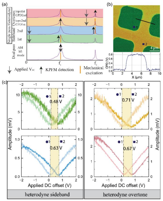
We demonstrate for the first time the in-situ implementation of single-pass heterodyne Kelvin probe force microscopy inside a scanning electron microscope, using piezo-resistive cantilevers. We overcome the capacitive crosstalk prevalent in piezo-resistive cantilevers by demodulating excitation and detection to simultaneously map surface topography and contact potential difference for correlation with compositional analysis. We systematically compare different operational modes of this heterodyne technique, elucidating their spatial resolution, signal sensitivity, and signal-to-noise ratio. The integrated approach yields exceptional signal quality and reveals how electron beam scan params.
What carries the argument
Heterodyne KPFM with demodulated excitation and detection frequencies on piezo-resistive cantilevers, which separates the electrical signals to cancel crosstalk while recording topography and contact potential difference in one scan.
Load-bearing premise
Demodulating the excitation and detection frequencies fully removes capacitive crosstalk in piezo-resistive cantilevers without adding new artifacts or lowering spatial resolution.
What would settle it
Run the demodulated heterodyne mode on a flat sample with uniform known contact potential and check whether the potential map stays constant or instead shows repeating patterns tied to cantilever motion or the SEM scan lines.
Figures


read the original abstract
Correlative nanoscale surface characterization benefits from simultaneously measuring electronic and structural properties in the same environment, a capability that is essential for modern-day materials science and semiconductor failure analysis. In-situ AFM-SEM measurements facilitated by self-sensing cantilevers offer great potential here; however, they are limited due to their inherent capacitive crosstalk. Here, we demonstrate for the first time the in-situ implementation of single-pass heterodyne Kelvin probe force microscopy inside a scanning electron microscope, using piezo-resistive cantilevers. We overcome the capacitive crosstalk prevalent in piezo-resistive cantilevers by demodulating excitation and detection to simultaneously map surface topography and contact potential difference for correlation with compositional analysis. We systematically compare different operational modes of this heterodyne technique, elucidating their spatial resolution, signal sensitivity, and signal-to-noise ratio. The integrated approach yields exceptional signal quality and reveals how electron beam scan parameters can directly influence surface potential contrast. We demonstrate this correlative analysis workflow on two-dimensional heterostructures and semiconductor circuits. This work establishes a robust and versatile correlative imaging mode for in-situ Kelvin force and topography imaging inside a scanning electron microscope for next-generation semiconductor device analysis and materials science.
Editorial analysis
A structured set of objections, weighed in public.
Referee Report
Summary. The manuscript describes the first in-situ implementation of single-pass heterodyne Kelvin probe force microscopy (KPFM) inside a scanning electron microscope using piezo-resistive cantilevers. The central technical advance is the use of frequency demodulation on both excitation and detection to suppress capacitive crosstalk, thereby enabling simultaneous acquisition of topography and contact potential difference (CPD) maps. The authors report systematic comparisons of operational modes with respect to spatial resolution, sensitivity and signal-to-noise ratio, demonstrate the influence of SEM beam parameters on surface-potential contrast, and apply the workflow to 2D heterostructures and semiconductor circuits.
Significance. If the crosstalk suppression is shown to be robust and free of new artifacts, the work would provide a practical correlative platform that combines structural and electronic information in a single vacuum environment. Such capability is directly relevant to failure analysis and materials characterization in mesoscopic and 2D systems. The experimental demonstrations on real devices constitute a concrete strength.
major comments (2)
- [§3.2] §3.2 (Heterodyne KPFM implementation): the assertion that demodulating excitation and detection frequencies 'fully overcomes' capacitive crosstalk in piezo-resistive cantilevers is load-bearing for the central claim, yet the manuscript provides neither before/after crosstalk spectra nor a quantified suppression factor measured on a reference equipotential surface. Without these data it remains unclear whether residual coupling (including beam-induced or chamber-electronics paths) persists or whether the technique trades crosstalk for reduced effective bandwidth.
- [§4.1] §4.1 (Mode comparison): the reported spatial-resolution, sensitivity and SNR values for the different heterodyne modes are presented without error bars or statistical detail on the number of independent measurements; this weakens the quantitative comparison that underpins the recommendation of a preferred operating regime.
minor comments (2)
- [Figure 2] Figure 2 caption: the scale bars and color-bar units for CPD maps should be stated explicitly rather than left to the reader to infer from the text.
- The manuscript would benefit from a short table summarizing the key performance metrics (resolution, SNR, crosstalk level) across the compared modes.
Simulated Author's Rebuttal
We thank the referee for the constructive comments and positive evaluation of the significance of our work. We address each major comment below and have revised the manuscript to incorporate the suggested improvements.
read point-by-point responses
-
Referee: [§3.2] §3.2 (Heterodyne KPFM implementation): the assertion that demodulating excitation and detection frequencies 'fully overcomes' capacitive crosstalk in piezo-resistive cantilevers is load-bearing for the central claim, yet the manuscript provides neither before/after crosstalk spectra nor a quantified suppression factor measured on a reference equipotential surface. Without these data it remains unclear whether residual coupling (including beam-induced or chamber-electronics paths) persists or whether the technique trades crosstalk for reduced effective bandwidth.
Authors: We agree that explicit before/after spectra and a quantified suppression factor would strengthen the central claim. In the revised manuscript we have added crosstalk spectra acquired on a reference equipotential surface, together with a measured suppression factor exceeding two orders of magnitude. These data confirm that residual coupling, including any beam-induced or chamber-electronics contributions, remains below the noise floor of the measurement. We also show that the effective bandwidth after demodulation is still adequate for the scan rates employed, as demonstrated by the unchanged topographic resolution in the presented images. revision: yes
-
Referee: [§4.1] §4.1 (Mode comparison): the reported spatial-resolution, sensitivity and SNR values for the different heterodyne modes are presented without error bars or statistical detail on the number of independent measurements; this weakens the quantitative comparison that underpins the recommendation of a preferred operating regime.
Authors: We acknowledge that the quantitative comparisons would be more robust with statistical detail. In the revised manuscript we have added error bars to all reported values for spatial resolution, sensitivity and SNR. These are derived from at least five independent measurements per mode, and we have included a supplementary table listing the number of repetitions and standard deviations. The updated data continue to support the recommendation of the preferred operating regime. revision: yes
Circularity Check
No significant circularity in experimental instrumentation demonstration
full rationale
This is an experimental instrumentation paper focused on physical implementation of heterodyne KPFM inside an SEM using piezo-resistive cantilevers. The central claims rest on hardware setup, frequency demodulation to address crosstalk, and empirical comparisons of resolution/SNR across modes, with no mathematical derivation chain, fitted parameters, or equations that reduce to self-definition. No load-bearing self-citations or ansatz smuggling appear in the provided text; the result is supported by direct measurement rather than circular reduction to inputs.
Axiom & Free-Parameter Ledger
axioms (1)
- domain assumption Standard assumptions of force microscopy and electron imaging physics hold in the combined setup
Lean theorems connected to this paper
-
IndisputableMonolith/Cost/FunctionalEquation.leanwashburn_uniqueness_aczel unclear?
unclearRelation between the paper passage and the cited Recognition theorem.
We overcome the capacitive crosstalk prevalent in piezo-resistive cantilevers by demodulating excitation and detection to simultaneously map surface topography and contact potential difference
-
IndisputableMonolith/Foundation/RealityFromDistinction.leanreality_from_one_distinction unclear?
unclearRelation between the paper passage and the cited Recognition theorem.
single-pass heterodyne Kelvin probe force microscopy inside a scanning electron microscope, using piezo-resistive cantilevers
What do these tags mean?
- matches
- The paper's claim is directly supported by a theorem in the formal canon.
- supports
- The theorem supports part of the paper's argument, but the paper may add assumptions or extra steps.
- extends
- The paper goes beyond the formal theorem; the theorem is a base layer rather than the whole result.
- uses
- The paper appears to rely on the theorem as machinery.
- contradicts
- The paper's claim conflicts with a theorem or certificate in the canon.
- unclear
- Pith found a possible connection, but the passage is too broad, indirect, or ambiguous to say the theorem truly supports the claim.
Reference graph
Works this paper leans on
- [1]
-
[2]
M. P. Murrell, M. E. Welland, S. J. O’Shea, T. M. H. Wong, J. R. Barnes, A. W. McKinnon, M. Heyns, and S. Verhaverbeke, Applied Physics Letters 62, 786 (1993)
work page 1993
- [3]
- [4]
-
[5]
M. Radmacher, R. W. Tillmann, M. Fritz, and H. E. Gaub, Science 257, 1900 (1992)
work page 1900
-
[6]
S. R. Cohen, Ultramicroscopy 42–44, 66 (1992)
work page 1992
- [7]
- [8]
- [9]
- [10]
-
[11]
M. Nonnenmacher, M. P. O’Boyle, and H. K. Wickramasinghe, Applied Physics Letters 58, 2921 (1991)
work page 1991
-
[12]
S. V. Kalinin and D. A. Bonnell, Phys. Rev. B 63, 125411 (2001)
work page 2001
-
[15]
L. Collins, A. Belianinov, S. Somnath, N. Balke, S. V. Kalinin, and S. Jesse, Sci Rep 6, 30557 (2016)
work page 2016
-
[17]
A. Zahmatkeshsaredorahi, R. Millan-Solsona, D. S. Jakob, L. Collins, and X. G. Xu, Nat Rev Methods Primers 5, 53 (2025)
work page 2025
-
[18]
P. Xu, P. Wang, M. Wang, F. Sun, J. Leng, Y. Shi, S. Jin, and W. Tian, Nano-Micro Lett. 17, 285 (2025)
work page 2025
-
[19]
Y. Martin and H. K. Wickramasinghe, Applied Physics Letters 50, 1455 (1987)
work page 1987
-
[20]
H. J. Mamin, D. Rugar, J. E. Stern, B. D. Terris, and S. E. Lambert, Applied Physics Letters 53, 1563 (1988)
work page 1988
-
[21]
O. Kazakova, R. Puttock, C. Barton, H. Corte-León, M. Jaafar, V. Neu, and A. Asenjo, Journal of Applied Physics 125, 060901 (2019)
work page 2019
- [22]
-
[23]
C. C. Williams, W. P. Hough, and S. A. Rishton, Applied Physics Letters 55, 203 (1989)
work page 1989
- [24]
-
[25]
O. O. Maryon, C. M. Efaw, F. W. DelRio, E. Graugnard, M. F. Hurley, and P. H. Davis, JoVE 64102 (2022)
work page 2022
-
[26]
C. Wang, H. Jin, and Y. Zhao, Small 17, 2100974 (2021)
work page 2021
-
[27]
C. Sakaguchi, Y. Nara, T. Hashishin, H. Abe, M. Matsuda, S. Tsurekawa, and H. Kubota, Sci Rep 10, 17055 (2020)
work page 2020
- [28]
- [29]
-
[30]
P. P. Swain, M. Penedo, and G. E. Fantner, Microscopy and Microanalysis 31, ozaf110 (2025)
work page 2025
-
[31]
C. H. Schwalb, A. Alipour, K. T. Arat, R. K. Dumas, D. Jangid, Md. A. R. Laskar, S. Chakrabarti, W. K. Neils, S. Sen, S. Spagna, and U. Celano, Applied Physics Reviews 12, 041314 (2025)
work page 2025
-
[32]
Lord Kelvin, The London, Edinburgh, and Dublin Philosophical Magazine and Journal of Science 46, 82 (1898)
-
[33]
U. Zerweck, C. Loppacher, T. Otto, S. Grafström, and L. M. Eng, Phys. Rev. B 71, 125424 (2005)
work page 2005
-
[34]
M. Fang, Y. Liu, T. Zhang, D. Wang, Z. Mai, and G. Xing, Applied Physics Letters 126, 173504 (2025)
work page 2025
-
[35]
C. Xiao, C. Wang, W. Ke, B. P. Gorman, J. Ye, C.-S. Jiang, Y. Yan, and M. M. Al-Jassim, ACS Appl. Mater. Interfaces 9, 38373 (2017)
work page 2017
-
[36]
C. M. Efaw, T. Da Silva, P. H. Davis, L. Li, E. Graugnard, and M. F. Hurley, J. Electrochem. Soc. 166, C3018 (2019)
work page 2019
-
[37]
M. F. Hurley, C. M. Efaw, P. H. Davis, J. R. Croteau, E. Graugnard, and N. Birbilis, CORROSION 71, 160 (2015)
work page 2015
- [38]
-
[39]
M. Tortonese, H. Yamada, R. C. Barrett, and C. F. Quate, in TRANSDUCERS ’91: 1991 International Conference on Solid-State Sensors and Actuators. Digest of Technical Papers (IEEE, San Francisco, CA, USA, 1991), pp. 448–451
work page 1991
- [40]
-
[41]
T. Gotszalk, P. Grabiec, F. Shi, P. Dumania, P. Hudek, and I. W. Rangelow, Microelectronic Engineering 41–42, 477 (1998)
work page 1998
- [42]
-
[43]
A. J. Haemmerli, N. Harjee, M. Koenig, A. G. F. Garcia, D. Goldhaber-Gordon, and B. L. Pruitt, Journal of Applied Physics 118, 034306 (2015)
work page 2015
-
[46]
S. P. Ramanandan, P. Tomić, N. P. Morgan, A. Giunto, A. Rudra, K. Ensslin, T. Ihn, and A. Fontcuberta I Morral, Nano Lett. 22, 4269 (2022)
work page 2022
-
[47]
Nenovision, Microscopy Today 30, 18 (2022)
work page 2022
- [48]
-
[49]
Quantum Design, Microscopy Today 31, 22 (2023)
Inc. Quantum Design, Microscopy Today 31, 22 (2023)
work page 2023
-
[50]
Quantum Design, (2023)
work page 2023
-
[51]
S. H. Andany, G. Hlawacek, S. Hummel, C. Brillard, M. Kangül, and G. E. Fantner, Beilstein J. Nanotechnol. 11, 1272 (2020)
work page 2020
- [52]
- [53]
-
[54]
J. Schindelin, I. Arganda-Carreras, E. Frise, V. Kaynig, M. Longair, T. Pietzsch, S. Preibisch, C. Rueden, S. Saalfeld, B. Schmid, J.-Y. Tinevez, D. J. White, V. Hartenstein, K. Eliceiri, P. Tomancak, and A. Cardona, Nat Methods 9, 676 (2012)
work page 2012
-
[55]
G. E. Fantner, D. J. Burns, A. M. Belcher, I. W. Rangelow, and K. Youcef-Toumi, Journal of Dynamic Systems, Measurement, and Control 131, 061104 (2009)
work page 2009
-
[56]
Ch. Sommerhalter, Th. W. Matthes, Th. Glatzel, A. Jäger-Waldau, and M. Ch. Lux-Steiner, Applied Physics Letters 75, 286 (1999)
work page 1999
-
[57]
A. Zahmatkeshsaredorahi, D. S. Jakob, and X. G. Xu, J. Phys. Chem. C 128, 9813 (2024)
work page 2024
-
[58]
H. Xie, H. Zhang, D. Hussain, X. Meng, J. Song, and L. Sun, Langmuir 33, 2725 (2017)
work page 2017
- [59]
- [60]
-
[61]
R. Coq Germanicus, M. Chaudhary, E. Vuillermet, and M. Lazar, in (2025), pp. 404–410
work page 2025
- [62]
-
[63]
Z. Peng, X. Chen, Y. Fan, D. J. Srolovitz, and D. Lei, Light Sci Appl 9, 190 (2020)
work page 2020
- [64]
-
[65]
X. Liu, B. Erbas, A. Conde-Rubio, N. Rivano, Z. Wang, J. Jiang, S. Bienz, N. Kumar, T. Sohier, M. Penedo, M. Banerjee, G. Fantner, R. Zenobi, N. Marzari, A. Kis, G. Boero, and J. Brugger, Nat Commun 15, 6934 (2024)
work page 2024
-
[66]
J. D. Adams, B. W. Erickson, J. Grossenbacher, J. Brugger, A. Nievergelt, and G. E. Fantner, Nature Nanotech 11, 147 (2016)
work page 2016
-
[67]
Z. Qu, J. Wei, Y. Sugawara, and Y. Li, Surfaces and Interfaces 49, 104441 (2024)
work page 2024
-
[68]
Günther, Progress in Surface Science 70, 187 (2002)
S. Günther, Progress in Surface Science 70, 187 (2002)
work page 2002
-
[69]
H. J. Leamy, Journal of Applied Physics 53, R51 (1982)
work page 1982
-
[70]
C. F. Mallinson, A. Harvey, and J. F. Watts, J. Electrochem. Soc. 164, C342 (2017). Supplementary information Different H-KPFM configurations for a tri-layer polymer piezo-resistive sensing cantilever in vacuum Effect of the electron beam and the ion beam observed with in-situ KPFM imaging Supplementary figures S1: Process flow and cantilever pictures S2:...
work page 2017
-
[71]
N. Hosseini, M. Neuenschwander, J. D. Adams, S. H. Andany, O. Peric, M. Winhold, M. C. Giordano, V. S. Bhat, M. Penedo, D. Grundler, and G. E. Fantner, Nat Electron 7, 567 (2024)
work page 2024
-
[72]
J. L. Garrett and J. N. Munday, Nanotechnology 27, 245705 (2016)
work page 2016
-
[73]
Y. Sugawara, L. Kou, Z. Ma, T. Kamijo, Y. Naitoh, and Y. Jun Li, Applied Physics Letters 100, 223104 (2012)
work page 2012
-
[74]
J. R. Lozano, D. Kiracofe, J. Melcher, R. Garcia, and A. Raman, Nanotechnology 21, 465502 (2010)
work page 2010
- [75]
-
[76]
S.-J. Park, J. C. Doll, and B. L. Pruitt, J. Microelectromech. Syst. 19, 137 (2010)
work page 2010
- [77]
- [78]
-
[79]
S. Hettler, M. Dries, P. Hermann, M. Obermair, D. Gerthsen, and M. Malac, Micron 96, 38 (2017)
work page 2017
-
[80]
M. Hugenschmidt, K. Adrion, A. Marx, E. Müller, and D. Gerthsen, Microscopy and Microanalysis 29, 219 (2023)
work page 2023
-
[81]
C. F. Mallinson and J. F. Watts, J. Electrochem. Soc. 163, C420 (2016)
work page 2016
-
[82]
M. A. Stevens-Kalceff, MRS Proc. 738, G5.4 (2002)
work page 2002
-
[83]
M. Kovařík, D. Citterberg, E. Paiva De Araújo, T. Šikola, and M. Kolíbal, ACS Appl. Electron. Mater. 6, 8776 (2024)
work page 2024
-
[84]
M. A. Stevens-Kalceff, S. Rubanov, and P. R. Munroe, MRS Online Proceedings Library 792, 74 (2003)
work page 2003
-
[85]
C. A. Volkert and A. M. Minor, MRS Bull. 32, 389 (2007)
work page 2007
discussion (0)
Sign in with ORCID, Apple, or X to comment. Anyone can read and Pith papers without signing in.