REVIEW 3 major objections 4 minor 28 references
Meyer-Neldel and anti-Meyer-Neldel rule in microcrystalline silicon and silicon carbide examined with Hall measurements
T0 review · 3 major / 4 minor · reviewed 2026-08-14 · deepseek-v4-flash
Pith's one-line read A single microcrystalline silicon sample switches between Meyer–Neldel and anti-Meyer–Neldel behavior when its defect density changes, tying the rule to Fermi-level position.
desk verdict A useful experimental paper with a clever theoretical framing, but the headline 'first sample switching' rests on a by-eye split of six points and needs statistical backup before it can be believed. read the letter →
The pith
A machine-rendered reading of the paper's core claim, the machinery that carries it, and where it could break.
The reading
What carries the argument
The central object is the Meyer–Neldel rule itself, the observation that Arrhenius prefactors grow exponentially with activation energy so that extrapolated Arrhenius lines meet at one point, together with its negative-slope counterpart anti-MNR. The theoretical machinery is the statistical-shift model, which predicts MNR for carrier concentration because the Fermi level moves with temperature. The paper shows this model alone does not give MNR in conductivity; the mobility must meet one of three conditions. The load-bearing condition in this work is the empirical proportionality $E_n^a = a\,E_\mu^a + b$, observed with $a \approx 1.25$ and $b \approx -18$ meV in the anti-MNR domain of both $\mu$c-Si:H and $\mu$c-SiC:H. Substituting this relation into the Arrhenius forms for $n$ and $\mu$ yields the room-temperature power law $\mu_r(n_r) = \mu'_{00} (n_r/n_{00})^\kappa$ with $\kappa = E^n_{MN}(E^\mu_{MN} - kT_r)/(a\,E^\mu_{MN}(E^n_{MN} - kT_r))$.
What would settle it
Measure Hall transport on a sample whose defect density is stepped finely across the anti-MNR-to-MNR boundary: if the exponent $\kappa$ in $\mu_r(n_r)$ changes with the transition, or if $E_n^a$ versus $E_\mu^a$ stops lying on the $1.25$ slope line, then the derived power law and the claim that this proportionality governs the anti-MNR domain are wrong.
Extended reading notes
Core claim
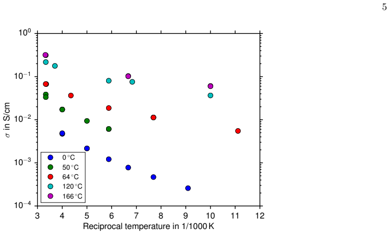
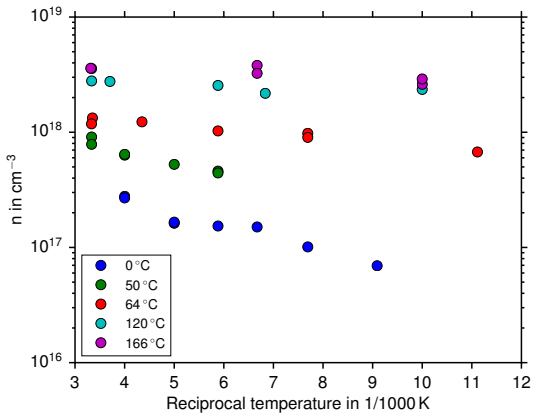
Using Hall measurements on seven microcrystalline silicon layers, one amorphous layer, two irradiated-and-annealed silicon samples, and five silicon carbide layers, the paper establishes three results. First, all three transport quantities—conductivity, carrier concentration, and mobility—show anti-Meyer–Neldel behavior in lightly doped microcrystalline silicon, and silicon carbide shows anti-MNR in conductivity and carrier concentration with Meyer–Neldel prefactors and energies close to silicon's. Second, the 15 ppm sample Ma-15 moves from the anti-MNR branch to the normal MNR branch as annealing removes bombardment-induced defects; the authors state this is the first report of such a transition by changing material properties, and take it as evidence that Fermi-level position controls MNR. Third, in the anti-MNR domain, the activation energies for carrier concentration and mobility obey a common linear relation $E_n^a = 1.25\,E_\mu^a - 18$ meV for both materials; combined with anti-MNR this yields a power law $\mu_r(n_r) \propto n_r^\kappa$, with $\kappa$ between 0.5 and 1.5, which the annealed-sample data reproduce with exponents around 0.48 and 0.61.
Load-bearing premise
All the quantitative conclusions rest on treating the measured transport as a single channel with well-defined activation energies, even though the temperature plots bend and the paper says the cause of the bending is speculative.
Editorial extensions
If this is right
- A fixed sample can be moved across the Meyer–Neldel/anti-Meyer–Neldel boundary solely by changing its defect density, so Fermi-level position, not sample identity, is what selects the regime.
- Observing MNR in conductivity is not automatic once carrier concentration follows the statistical shift; the mobility activation energy must satisfy one of three stated conditions, and in these data it does so through the linear $E_n^a$–$E_\mu^a$ relation.
- Silicon carbide joins silicon with nearly the same anti-MNR parameters, strengthening the case for a common Meyer–Neldel behavior across disordered semiconductors.
- The derived power law $\mu_r \propto n_r^\kappa$ with $\kappa$ between 0.5 and 1.5 gives a compact way to predict room-temperature mobility from carrier concentration in the anti-MNR regime.
- The unresolved item the paper leaves open is a microscopic explanation for why $E_n^a$ and $E_\mu^a$ are proportional in the first place.
Reading between the lines
- If the proportionality $E_n^a = 1.25\,E_\mu^a - 18$ meV holds beyond these two material families, then the ratio between carrier-concentration and conductivity Meyer–Neldel energies (about 1.7 here) should be derivable from that line alone; a future analysis could check that consistency.
- The same-sample switch suggests a device-relevant handle: irradiation and low-temperature annealing can toggle a film's transport regime without changing its chemistry.
- A sharper test than the paper's would fix the exact defect densities and measure $\kappa$ continuously across the anti-MNR-to-MNR boundary; if $\kappa$ is constant within the anti-MNR branch, the power-law picture is robust, and if it drifts, the boundary is not a clean phase-like division.
- Because the paper lists barrier-height distributions and differential mobility as alternative causes of the Arrhenius curvature, a natural next step is to check whether either mechanism also predicts the measured $E_n^a$–$E_\mu^a$ slope; if one does, it would unify the curvature and the power law.
Signed reviews
Editorial analysis
A structured set of objections, weighed in public.
Referee Report
Summary. The paper reports temperature-dependent Hall measurements of conductivity, carrier concentration, and mobility for lightly phosphorus-doped microcrystalline silicon (μc-Si:H) and hydrogenated silicon carbide (μc-SiC:H), including a series of electron-irradiated μc-Si:H samples measured after step-wise annealing. The authors analyze the data in Meyer-Neldel rule (MNR) plots and report anti-MNR behavior for most samples, the first observation of anti-MNR in μc-SiC:H, and a claim that a single μc-Si:H sample (Ma-15) switches from anti-MNR to normal MNR as its defect density is changed by annealing. The theoretical part of the paper shows that MNR in the carrier concentration does not by itself imply MNR in conductivity unless the mobility satisfies one of three conditions, identifies the proportionality E_n^a = a E_μ^a + b as the operative condition, and derives from it a power-law relation between room-temperature mobility and carrier concentration, μ_r = μ'_00 (n_r/n_00)^κ.
Significance. If the empirical claims hold, the paper provides a valuable experimental dataset that extends the MNR phenomenology: the first reported anti-MNR in μc-SiC:H, a systematic comparison of MNR in σ, n, and μ for the same samples, and a claimed single-sample transition between anti-MNR and MNR that would support the Fermi-level position as the controlling parameter. The theoretical derivation connecting the linear E_n^a-E_μ^a relation to a μ(n) power law is a useful formal step, even though its practical value depends on the independence of the fitted parameters. The paper also gives credit by explicitly flagging the speculative origin of the Arrhenius curvature and the large uncertainties in the mobility data, which is appropriate for a study of this type.
major comments (3)
- [IV A, Fig. 5] The central claim that sample Ma-15 switches from anti-MNR to normal MNR is based on a visual dichotomy of six data points, three assigned to the anti-MNR line and three to a dashed 'guide to the eye' for normal MNR. No fit is reported for the right-hand group, no goodness-of-fit test is compared with the anti-MNR line, and the text states that these points have 'larger error estimates.' The authors should quantify whether the three right-hand points are statistically incompatible with the anti-MNR line fitted from the annealed samples, including the effects of the large error bars and of the choice of Arrhenius fit window, before the switching claim can be accepted.
- [V B, Eq. (7) and Fig. 9] The power-law exponent κ in Eq. (7) is computed from E^n_MN, E^μ_MN, a, and b, all of which are fitted from the same Hall data used to produce Fig. 9. The subsequent fit of κ in Fig. 9 (values 0.48 and 0.61) is therefore not an independent test of the derived relation; it only checks that the direct fit lies in the broad range allowed by the large uncertainties. The authors should either provide a proper uncertainty propagation for κ and state whether the directly fitted exponents are consistent with the derived values under that propagation, or clearly label the power law as a consistency check rather than a prediction.
- [III and Figs. 5-8] The MNR coordinates (activation energy and prefactor) are extracted from Arrhenius curves that are explicitly convex rather than straight, and the text concedes that the cause of the curvature is speculative. Because each MNR point depends on the local slope and intercept at room temperature, the classification of samples into MNR and anti-MNR regimes, including the claimed Ma-15 switching, is sensitive to the fitting procedure. The manuscript should specify the exact fitting window and method, and ideally show how the MNR plot changes when the window is varied within the measurement range, so that the reader can assess whether the reported separation is robust.
minor comments (4)
- [IV A] The text states that the demarcation between MNR and anti-MNR lies at 'approx. 120 eV'; this should presumably be 120 meV.
- [II B and Fig. 9] There are typographical errors: 'degration' in Section II B, 'poylnomial' in the caption of Fig. 9, and 'suprising' in Section IV B. The sample identifiers '05B-054' and '06B-276' in Section V B are not defined in the paper.
- [Appendix A] The appendix title says 'at root temperature'; this should be 'at room temperature.'
- [V A, Eq. (4)] The notation 'terms without Ea’s' is imprecise; the authors should state explicitly which constants (such as n_00 and μ_00) are absorbed into the y-intercept, to make the derivation easier to follow.
Circularity Check
The derived µ(n) power law is a rearrangement of fitted MNR parameters and the fitted E_n–E_µ relation; the experimental MNR and switching observations themselves are not circular.
-
fitted input called prediction
[Section V B, Eqs. (5)–(7), Fig. 9, and Appendix A]
"This polynomial relation can be derived from the presence of anti-MNR and the linear dependence of the activation energies of n and µ: ... κ = ... with Tr being room temperature, a and b as defined in the previous section, and κ ranging between 0.5 and 1.5, in accordance with the large uncertainties in EnMN and EµMN. ... Fig. 9 ... The given values for κ represent the exponent of the polynomial fits ... and refer to Eq. 7."
The power-law exponent κ in Eq. 7 is expressed in terms of E^n_MN, E^µ_MN, a, and b. E^n_MN and E^µ_MN are fitted from the same annealed-sample Hall data (Table III, Figs. 6 and 7), and a and b are fitted from the same samples' E^n_a versus E^µ_a relation (Fig. 8, Eq. A3). The paper then presents Fig. 9, where κ is fitted again from the same room-temperature µ–n data, and accepts agreement only within the broad 0.5–1.5 range. Since the power law is an algebraic consequence of the Arrhenius/MNR forms and the fitted linear relation, any data set satisfying those fitted relations will by construction exhibit a power law with κ in that range. The 'derivation' therefore reduces to the fitted inputs rather than providing an independent prediction.
full rationale
The paper's empirical findings — anti-MNR for σ, n, and µ, the first anti-MNR observation in µc-SiC:H, and the claimed same-sample MNR/anti-MNR switching — are direct descriptions of Hall measurements and are not circular in themselves; they stand or fall on data quality and statistical analysis. The circularity lies in the theoretical section. The claimed derivation of the µ(n) power law (Eq. 5) uses parameters that are all fitted from the same dataset: the Meyer-Neldel energies from the anti-MNR fits of the annealed samples (Table III) and the slope/intercept a and b of the E^n_a–E^µ_a proportionality (Fig. 8). Inserting these fitted values into Eq. 7 gives κ, and Fig. 9 then fits κ from the same room-temperature n–µ points, comparing only against the loose 0.5–1.5 interval. This is not an independent test but a consistency check, and the 'prediction' is forced by the construction of the equations. I did not find other load-bearing circular steps: the statistical-shift assumption is a stated modeling choice, and the self-citations (e.g., Ref. 13 for previously published Hall data) are not relied on as the sole justification for any central result. The score of 6 reflects partial circularity affecting the theoretical derivation while the core experimental observations retain independent content.
Assumptions & free parameters
free parameters (6)
- E^sigma_MN (anti-MNR energy for conductivity) =
-17 +/- 6 meV
- E^n_MN (anti-MNR energy for carrier concentration) =
-29 +/- 3 meV
- a (slope of E_n vs E_mu) =
1.25
- b (intercept of E_n vs E_mu) =
-18 meV
- E^mu_MN (anti-MNR energy for mobility) =
not reliably determined
- demarcation activation energy between MNR and anti-MNR =
approx. 120 meV
assumptions (5)
- domain assumption The statistical shift model describes the temperature dependence of carrier concentration n in these samples.
- domain assumption Each sample is characterized by single activation energies E_n and E_mu over the fitted temperature window.
- ad hoc to paper The relation E_n = a E_mu + b is linear and holds for all anti-MNR samples.
- domain assumption Hall measurements yield the true free-carrier concentration n and mobility mu.
- domain assumption The mobility has a nonzero activation energy E_mu, so mobility-edge theory with mu ~ T^-1 does not apply.
Cite this review
Pith. "Pith review of Meyer-Neldel and anti-Meyer-Neldel rule in microcrystalline silicon and silicon carbide examined with Hall measurements." pith.science (2026). https://pith.science/paper/EXGJHB7K
@misc{pith2026190806516,
  author       = {Pith},
  title        = {Pith review of: Meyer-Neldel and anti-Meyer-Neldel rule in microcrystalline silicon and silicon carbide examined with Hall measurements},
  year         = {2026},
  howpublished = {\url{https://pith.science/paper/EXGJHB7K}},
  note         = {Machine review of arXiv:1908.06516}
}
abstract
We study the electronic transport in lightly phosphorus-doped hydrogenated microcrystalline silicon ($\mu$c-Si:H) and nominally undoped hydrogenated silicon carbide ($\mu$c-SiC:H) by temperature-dependent Hall measurements. The material properties cover different crystallinities and doping concentrations. For$\mu$c-Si:H samples, the carrier concentration is altered by electron bombardment and subsequent step-wise annealing of defects. We describe the behavior of conductivity, mobility, and carrier concentration in terms of the Meyer-Neldel rule (MNR) and anti-MNR. We present the first sample switching between them. A theoretical examination leverages the anti-MNR to describe electronic room temperature properties, and it expands the statistical shift model.
Figures

Figures from the paper (6 more)


Reference graph
Works this paper leans on
- [1]
-
[2]
W. Fuhs, P. Kanschat, and K. Lips, Journal of Vacuum Science & Technology B: Microelectronics and Nanometer Structures 18, 17921795 (2000)
work page 2000
-
[3]
The respective MNR energies for σ are:
En a =a·Eµ a +b Here, a and b are parameters of the linear dependence. The respective MNR energies for σ are:
-
[4]
Eσ MN = (a + 1) En MNEµ MN aEµ MN +En MN Thus, the statistical Fermi level shift is not sufficient for the occurrence of some form of MNR in σ. Additionally, the mobility must fulfill at least one of the three conditions. Generally, examinations of the MNR in disordered semiconductors implicitly assume (1), i. e. a very weak temper- ature dependence of mobil...
-
[5]
W. v. Meyer and H. Neldel, Z. tech. Phys 18, 588 (1937)
1937
- [6]
-
[7]
P. Thomas and H. Overhof, in Defect and Diffusion Forum , Vol. 192 (Trans Tech Publ, 2001) p. 114
work page 2001
-
[8]
S. K. Ram, S. Kumar, and P. Roca i Cabarrocas, Journal of Non-Crystalline Solids 354, 22632267 (2008)
work page 2008
Show all 28 references
-
[9]
S. K. Ram, S. Kumar, and P. R. i. Cabarrocas, in Materials Research Society Symposium Proceedings, Vol. 715 (Cambridge University Press, 2002) p. 357362
2002
-
[10]
Irsigler, D
P. Irsigler, D. Wagner, and D. Dunstan, Journal of Physics C: Solid State Physics 16, 6605 (1983)
1983
-
[11]
Overhof and W
H. Overhof and W. Beyer, Philosophical Magazine B 43, 433450 (1981)
1981
-
[12]
Overhof and W
H. Overhof and W. Beyer, Philosophical Magazine Part B 47, 377 (1983)
1983
-
[13]
Beyer and H
W. Beyer and H. Mell, in 7th Int. Conf. on Amorphous and Liquid Semiconductors , edited by W. E. Spear (1977) p. 333
1977
-
[14]
S. K. Ram, S. Kumar, and P. Roca i Cabarrocas, Journal of non-crystalline solids 352, 1172 (2006)
2006
-
[15]
The demarcation between both lies at approx. 120 eV, which is similar to other reports.[4, 5] The amorphous silicon sample (10 ppm/22 %) should also be considered being in the normal MNR regime, although it is the only representative of its type of material, so no clear classi...
-
[16]
Astakhov, R
O. Astakhov, R. Carius, Y. Petrusenko, V. Borysenko, D. Barankov, and F. Finger, in MRS Proceedings, Vol. 989 (Cambridge University Press, 2007) pp. 3–8
2007
-
[17]
Finger, O
F. Finger, O. Astakhov, T. Bronger, R. Carius, T. Chen, A. Dasgupta, A. Gordijn, L. Houben, Y. Huang, S. Klein, et al., Thin Solid Films 517, 3507 (2009)
2009
-
[18]
Bronger and R
T. Bronger and R. Carius, Thin Solid Films 515, 7486 (2007)
2007
-
[19]
B.-G. Yoon, C. Lee, and J. Jang, Journal of applied physics 60, 673 (1986)
1986
-
[20]
Werner, Solid State Phenomena 37, 213 (1994)
J. Werner, Solid State Phenomena 37, 213 (1994)
1994
-
[21]
Bronger, Electronic properties of µc-Si:H layers investigated with Hall measurements , Ph.D
T. Bronger, Electronic properties of µc-Si:H layers investigated with Hall measurements , Ph.D. thesis, RWTH Aachen, Germany (2007)
2007
-
[22]
Carius, F
R. Carius, F. Finger, U. Backhausen, M. Luysberg, P. Hapke, L. Houben, M. Otte, and H. Overhof, in MRS Proceedings, Vol. 467 (Cambridge University Press, 1997) p. 283
1997
-
[23]
J. C. Dyre, Journal of Physics C: Solid State Physics 19, 5655 (1986)
1986
-
[24]
Carius, J
R. Carius, J. M¨ uller, F. Finger, N. Harder, P. Hapke, J. Marshall, N. Kirov, A. Vavrek, and J. Maud, in Thin Film Materials and Devices-Developments in Science and Technology (1999) p. 157
1999
-
[25]
Lucovsky, C
G. Lucovsky, C. Wang, M. Williams, Y. Chen, and D. Mauer, in MRS Proceedings, Vol. 283 (Cambridge University Press,
-
[26]
Meiling and R
H. Meiling and R. Schropp, Applied physics letters 74, 10121014 (1999)
1999
-
[27]
N. F. Mott and E. A. Davis, Electronic processes in non-crystalline materials (Oxford University Press, 2012)
2012
-
[28]
Jackson, Physical Review B 38, 3595 (1988)
W. Jackson, Physical Review B 38, 3595 (1988)
1988
Reviewed August 14, 2026 · model on record in the stance chip above.
Discussion (0). Continue with ORCID to comment.