REVIEW 4 major objections 4 minor 78 references
Parasitic conduction channels in topological insulator thin films
T0 review · 4 major / 4 minor · reviewed 2026-08-14 · deepseek-v4-flash
Pith's one-line read The paper shows that the interior charge carrier density of a thin topological insulator film can be estimated from surface measurements alone, without knowing its dopant concentration.
desk verdict A practically useful band-bending recipe for TI thin-film transport, but the central dopant-independence claim is only marginally in its stated regime and the outputs are sensitive to inputs taken from the authors' own earlier analysis. read the letter →
The pith
A machine-rendered reading of the paper's core claim, the machinery that carries it, and where it could break.
The reading
What carries the argument
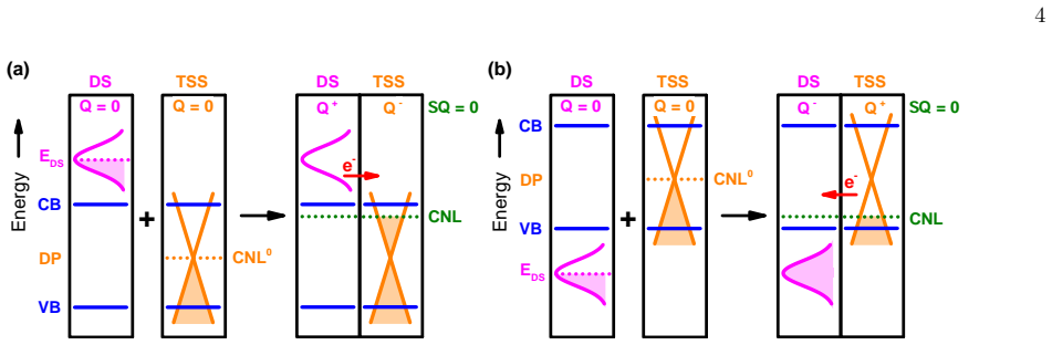
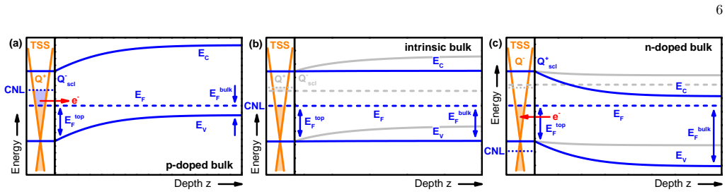
The central mechanism is the comparison between the Debye screening length $L=\sqrt{\epsilon_0\epsilon_r k_B T/(q^2(n_b+p_b))}$ and the film thickness $d$. When $d\ll L$, Poisson's equation produces only weak band bending, so the boundary conditions at the top and bottom surfaces, represented by the surface Fermi levels $E_F^{\rm top}$ and $E_F^{\rm bottom}$, control the carrier distribution in the film rather than the unknown dopant concentration. Around this screening argument, the paper builds a semi-classical Poisson-Schrödinger calculation: it solves Poisson's equation with charge neutrality between the topological surface states and the space-charge layer, renormalizes the effective densities of states using quantized subbands in a square or triangular well, and iterates once to a second Poisson solution. A separate but supporting element is the charge-neutrality-level picture of the surface, which explains how trivial defect states shift the effective filling level of the Dirac cone and hence the measured surface Fermi energy.
What would settle it
Grow thin TI films of the same material with intentionally varied dopant levels, for example by changing growth stoichiometry, while keeping the surface Fermi level fixed, and measure the interior sheet carrier density at zero gate voltage; if that density shifts by more than the calculation's predicted variation across the band gap, the screening-length assumption is violated and the dopant-independent estimate fails.
Extended reading notes
Core claim
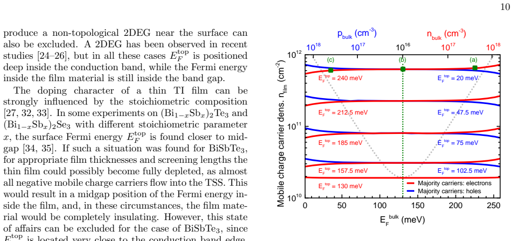
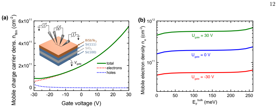
The paper establishes that in a thin topological insulator film, the top and bottom topological surface states exchange charge with the film interior until charge neutrality is reached, and because the Debye screening length $L$ far exceeds the film thickness $d$, the bands bend only weakly. As a result, a wide range of unintentional dopant concentrations leaves the band positions essentially fixed by the surface Fermi levels rather than by the bulk dopant density. The authors solve Poisson's equation for the band bending using symmetric boundary conditions (top and bottom surface Fermi levels equal) or asymmetric boundary conditions (top level from ARPES, bottom level extracted from gate-dependent four-point measurements), and they include confinement quantization through a square-well or triangular-well approximation of the band-bending potential. The integrated mobile carrier density $n_{\rm film}$ is then nearly flat as a function of the bulk Fermi energy across the band gap. For a 10 nm BiSbTe$_3$ film they obtain $n_{\rm film}\approx 6\times 10^{11}$ cm$^{-2}$ in the symmetric approximation and $\approx 2\times 10^{11}$ cm$^{-2}$ in the asymmetric approximation at zero gate voltage, with the latter being the more precise estimate. Combined with an interface conductivity measured on the bare substrate reconstruction before film growth, this allows the total measured 2D conductivity to be decomposed into surface-state, interior, interface, and substrate contributions.
Load-bearing premise
The calculation stands on the assumption that the film is much thinner than the screening length of its mobile charges, so band bending stays weak; if a material screens more efficiently, through a smaller dielectric constant, higher carrier density, or degenerate doping, the unknown dopant concentration would control the result.
Editorial extensions
If this is right
- Given an ARPES measurement of the top surface Fermi level, the interior mobile carrier density of a thin TI film can be estimated without knowing its unintentional dopant concentration.
- With additional gate-dependent four-point transport data, the asymmetric calculation gives a more precise value; for BiSbTe$_3$ at zero gate voltage this is about $2\times 10^{11}$ cm$^{-2}$, one third of the symmetric estimate.
- Because the interface conductivity can be measured on the bare substrate reconstruction before film growth, the total measured 2D conductivity can be decomposed into TSS, interior, interface, and substrate channels.
- The approach is presented as general across TI material classes, and the same gate-dependent measurements also yield the carrier mobility, so the interior conductivity itself becomes accessible.
- For device design, the results imply that low-conductivity substrate terminations such as Te/Si(111)-(1$\times$1) keep parasitic interface currents negligible, whereas Bi/Si(111)-(√3$\times$√3) would carry a substantial fraction of the current.
Reading between the lines
- A direct test of the claim would be to grow films with deliberately varied dopant concentrations and check that the interior sheet density stays on the flat plateau of the calculation's Fig. 5, rather than tracking the dopant level.
- The screening-length criterion $L\gg d$ offers a quick screening rule for other TI candidates: compute $L$ from the dielectric constant and intrinsic carrier density before investing in the full ARPES-plus-gate measurement program.
- Low-temperature transport, where the film interior mobility rises relative to the surface channels, would provide a sharper falsifier, because the calculated interior conductivity could be compared with measured four-point data at temperatures where the mobility difference separates the channels.
- The same logic could be extended to estimate the interior carrier density of other van-der-Waals thin films with large dielectric constants, not only topological insulators, as long as the weak-bending condition is met.
Signed reviews
Editorial analysis
A structured set of objections, weighed in public.
Referee Report
Summary. The manuscript proposes a semi-classical calculation of the band bending and mobile carrier density in the interior of thin topological-insulator films, using experimentally determined surface and interface Fermi levels as input. The authors solve Poisson's equation with Boltzmann statistics and a Debye screening length, treat symmetric (E_top^F = E_bottom^F) and asymmetric boundary conditions, add quantization via square or triangular infinite wells, and apply the model to a 10 nm BiSbTe3 film using parameters from earlier ARPES and gate-dependent four-probe measurements. The central claim is that in the thin-film limit d << L the band bending and integrated film carrier density n_film are nearly independent of the unknown dopant concentration (represented by E_bulk^F), so that n_film, and with a known mobility the film conductivity, can be estimated from surface-sensitive measurements alone. For the BiSbTe3 example, the symmetric approximation gives n_film ~ 6e11 cm^-2 and the asymmetric approximation ~2e11 cm^-2 at zero gate voltage.
Significance. If the central claim holds, the paper offers a practically useful way to quantify the parasitic film-interior conduction channel that otherwise contaminates transport studies of topological surface states. The analytic Poisson-band-bending framework, the explicit distinction between dopant concentration and mobile carrier density, and the use of ARPES and gate-dependent transport data as inputs are valuable strengths, and the authors are unusually explicit about their approximations. However, the quantitative usefulness of the results is conditional on assumptions that are acknowledged but not fully validated: the d << L screening regime for the specific film, the Boltzmann approximation at a Fermi level only 20 meV below the conduction band, and the reliability of E_bottom^F and the mobility imported from the earlier transport analysis. Because these assumptions directly affect the quoted numbers, the paper is more convincing as a methodological proposal than as a validated quantitative estimate.
major comments (4)
- [II.B.4, Eq. (3)] The central dopant-independence claim requires d << L, but for the paper's own BiSbTe3 parameters the condition is only marginal: with epsilon_r ≈ 100 and n_b + p_b = 4e17 cm^-3, Eq. (3) gives L ≈ 19 nm, only about twice the d = 10 nm film; a factor-two reduction in epsilon_r or a tenfold increase in doping makes L ≤ d. The paper provides no measured epsilon_r or n_b + p_b for the MBE film under consideration, so the regime in which Figs. 4 and 5 are claimed to be dopant-independent is asserted rather than demonstrated. Please quantify d/L over the plausible doping range and either restrict the claim to that range or provide direct evidence that the 10 nm BiSbTe3 film is in the d << L regime.
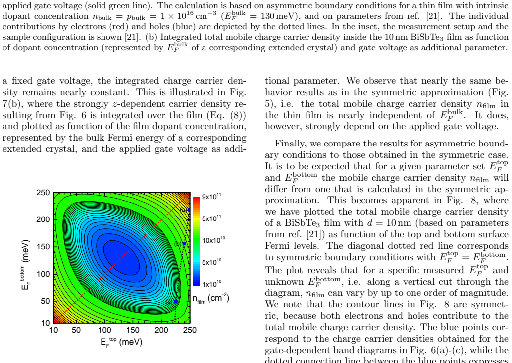
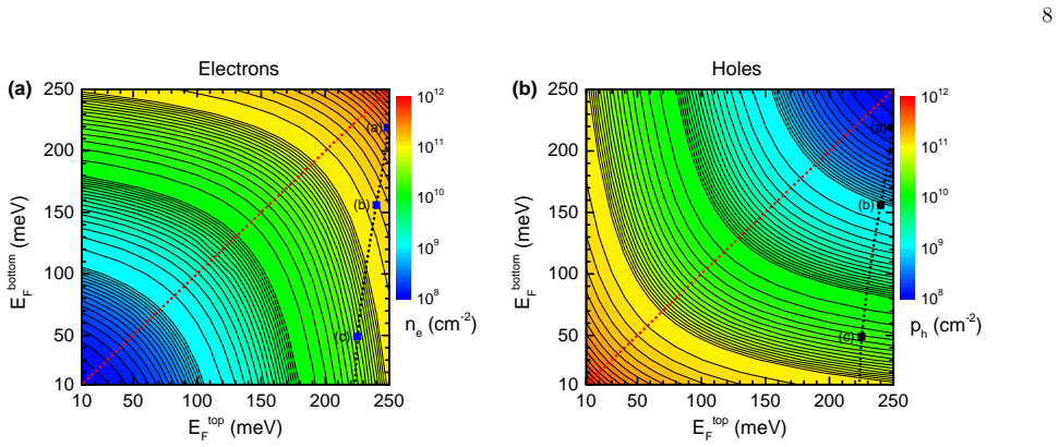
- [II.C, Fig. 8] The asymmetric result depends strongly on E_bottom^F, which is imported from the quantum-capacitance transport analysis of ref. [21]. For fixed E_top^F = 240 meV, n_film varies by up to an order of magnitude with E_bottom^F across the plotted range, and the symmetric and asymmetric values (6e11 vs 2e11 cm^-2) differ by a factor of three. If the ref. [21] analysis already determines the film channel's carrier density or conductivity, the asymmetric calculation is not an independent estimate; if it does not, the uncertainty in E_bottom^F should be propagated into n_film. Please state explicitly what ref. [21] provides and give an uncertainty budget for the quoted n_film values.
- [II.B.5] The Boltzmann approximation is knowingly used outside its validity for the example: E_top^F = 240 meV lies only 20 meV below the conduction-band edge, and the text concedes deviations of up to 50% from the Fermi-Dirac distribution. Since all quantitative values, including the factor 2 to 2.5 reduction from quantization and the final n_film estimates, are derived within this scheme, the paper should show at least one representative Fermi-Dirac calculation to demonstrate that the dopant-independence conclusion and the quoted n_film values survive.
- [II.B.2 and Supplemental Material B] The Schrödinger-Poisson self-consistency is truncated after one and a half iterations and wavefunction weighting is neglected. The authors state that these approximations may overestimate band bending near the surfaces and that quantization reduces n_film by a factor of 2 to 2.5 relative to the purely classical result. Because that factor materially changes the final estimates, a benchmark against a fully self-consistent solution for at least one parameter set is needed to establish the numerical accuracy of the method.
minor comments (4)
- [Table II] The value v_Fermi = 5.6 × 10^-5 ms^-1 appears to be a units typo; the Dirac velocity in a topological insulator should be several orders of magnitude larger, likely 5.6 × 10^5 m/s.
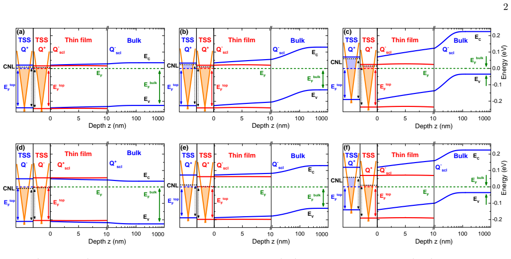
- [II.C and Fig. 6] The text says E_bottom^F = 156 meV at zero gate voltage while the Fig. 6 caption gives 155 meV; please make these values consistent.
- [Eq. (7)] The typeset equation contains garbled square-root and brace symbols and should be checked carefully in production.
- [II.B.7] The distinction between dopant concentration and mobile carrier density is helpful and should be kept; consider stating the definition of the 'bulk Fermi energy of a corresponding extended crystal' more prominently at first use.
Circularity Check
No significant circularity: the band-bending calculation is a genuine Poisson-equation solution with measured surface Fermi levels as boundary conditions, and the claimed dopant independence is an output, not an input.
full rationale
The paper's derivation chain is: (i) solve Poisson's equation (Eqs. 1-4) with the measured top Fermi level E_top^F from ARPES as a boundary condition; (ii) re-solve with quantized densities of states; (iii) integrate Eq. (8) to obtain the mobile carrier density n_film. The dopant independence of n_film is an output of this calculation (Figs. 4, 5, 7), not an input: E_bulk^F appears explicitly as a parameter in Eq. (8), and the calculation shows that n_film varies little with it in the d << L regime. E_top^F is an independently measured ARPES value from ref. [21]; E_bottom^F in the asymmetric branch is likewise an experimentally extracted input obtained from gate-dependent transport via quantum capacitance effects, and it is not the predicted quantity n_film. No equation in the paper defines n_film in terms of either surface Fermi level in a way that would make Eq. (8) an identity; Eq. (8) is a genuine integral over the calculated band profile. The reliance on ref. [21] for material parameters (m*, v_F, E_top^F, E_bottom^F, mobility) is self-citation, but those parameters are experimental inputs and are not derived from the quantity this paper claims to predict. The d << L regime is asserted for BiSbTe3 on the basis of a literature dielectric constant and assumed non-degenerate doping; if the regime fails, the dopant-independence claim would be incorrect, but that is a correctness or assumption risk, not circularity. The factor-of-three difference between symmetric and asymmetric results likewise indicates sensitivity to input assumptions, not that the output was fed back in. Since no specific reduction of the predicted quantity to its inputs could be quoted, no circular step is established.
Assumptions & free parameters
free parameters (3)
- E_bottom^F (bottom surface Fermi level at the interface) =
50 meV, 155 meV, 220 meV for gate voltages -30 V, 0 V, +30 V
- E_bulk^F (bulk Fermi level representing the unknown dopant concentration) =
35-225 meV in example calculations; 130 meV (intrinsic) in asymmetric estimates
- Charge carrier mobility in the TI film =
below 2 cm^2/Vs at room temperature for BiSbTe3
assumptions (7)
- standard math Poisson's equation and the standard semiconductor band-bending formalism apply to TI thin films.
- domain assumption The topological surface states do not pin the Fermi level, so E_top^F is a free boundary set by charge transfer between the TSS and the film.
- domain assumption In the symmetric approximation, the bottom TSS has the same filling level as the top TSS (E_top^F = E_bottom^F).
- domain assumption The Debye screening length is much larger than the film thickness for the relevant dopant range, so band bending is weak and nearly dopant-independent.
- ad hoc to paper The Poisson-Schrodinger cycle can be truncated after one and a half iterations, and quantization can be represented by square or triangular wells with infinite barriers, neglecting wavefunction weighting.
- domain assumption The Boltzmann distribution adequately describes mobile carriers even when E_top^F is only 20 meV below the conduction band edge.
- domain assumption The surface conductivity of the bare substrate reconstruction equals the interface conductivity beneath the TI film.
invented entities (1)
-
Surface charge neutrality level (CNL) of the combined TSS/defect-state system
Cite this review
Pith. "Pith review of Parasitic conduction channels in topological insulator thin films." pith.science (2026). https://pith.science/paper/EXUW7B6V
@misc{pith2026190809412,
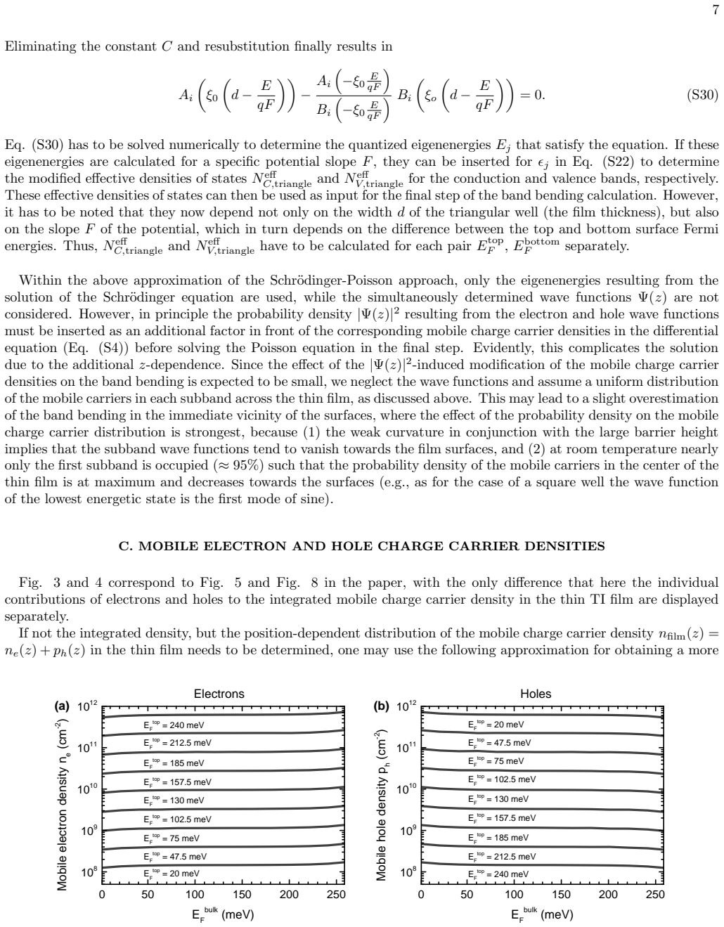
  author       = {Pith},
  title        = {Pith review of: Parasitic conduction channels in topological insulator thin films},
  year         = {2026},
  howpublished = {\url{https://pith.science/paper/EXUW7B6V}},
  note         = {Machine review of arXiv:1908.09412}
}
read the original abstract
Thin films of topological insulators (TI) usually exhibit multiple parallel conduction channels for the transport of electrical current. Beside the topologically protected surface states (TSS), parallel channels may exist, namely the interior of the not-ideally insulating TI film, the interface layer to the substrate, and the substrate itself. To be able to take advantage of the auspicious transport properties of the TSS, the influence of the parasitic parallel channels on the total current transport has to be minimized. Because the conductivity of the interior (bulk) of the thin TI film is difficult to access by measurements, we propose here an approach for calculating the mobile charge carrier concentration in the TI film. To this end, we calculate the near-surface band bending using parameters obtained experimentally from surface-sensitive measurements, namely (gate-dependent) four-point resistance measurements and angle-resolved photoelectron spectroscopy (ARPES). While in most cases another parameter in the calculations, i.e. the concentration of unintentional dopants inside the thin TI film, is unknown, it turns out that in the thin-film limit the band bending is largely independent of the dopant concentration in the film. Thus, a well-founded estimate of the total mobile charge carrier concentration and the conductivity of the interior of the thin TI film proves possible. Since the interface and substrate conductivities can be measured by a four-probe conductance measurement prior to the deposition of the TI film, the total contribution of all parasitic channels, and therefore also the contribution of the vitally important TSS, can be determined reliably.
Figures

Figures from the paper (11 more)




Reference graph
Works this paper leans on
-
[21]
H. Zhang, C.-X. Liu, X.-L. Qi, X. Dai, Z. Fang, and S.-C. Zhang, Nature Physics 5, 438 (2009)
work page 2009
-
[1]
Te/Si(111)-(7 ×7) For Te-based van-der-Waals epitaxy, a plausible inter- face reconstruction is the Te/Si(111)-(7 ×7) reconstruc- tion, which has been reported as a template for the growth of TI films on Si(111) [42]. It can be prepared at room temperature by depositing Te on top of a re- constructed Si(111)-(7×7) surface. In a first step, the (7×7)-reconst...
-
[2]
E F t op = 20 meVE F t op = 47.5 meVE F t op = 240 meVE F t op = 212.5 meVE F t op = 185 meVE F t op = 157.5 meVE F t op = 130 meVE F t op = 102.5 meVE F t op = 75 meV Majority carriers: electrons Majority carriers: holes1 01 8n b ulk ( c m-
-
[3]
pb ulk ( c m- 3) FIG. 5. (Color online) Integrated total mobile charge car- rier density nfilm based on the symmetric approximation for a thin TI film as function of the dopant concentration rep- resented by the bulk Fermi energy Ebulk F . The surface Fermi energy Etop F is an additional parameter. For Ebulk F inside the band-gap, the calculated film carrier...
-
[4]
This is immediately obvious from Eq
Screening The weak band bending in the thin TI film is linked to the long screening length L compared to the small film thickness d. This is immediately obvious from Eq. (2), which shows that the curvature of the band bending potential v is inversely proportional to the square of L. A small curvature of course also limits the value of v that can be reached ...
-
[5]
Degenerate doping In Fig. 4, only non-degenerate doping levels in the TI have been considered, all of which apparently lead to a downward band bending. Of course, it is in principle also possible that the dopant concentration is sufficiently high for the TI material to be degenerately n-doped, with Ebulk F above the conduction band edge. According to our ca...
-
[6]
BiSbTe 3, which was studied extensively in ref
The example of BiSbTe 3 Here, we focus on the specific TI material (Bi1−xSbx)2Te3 with x = 0 .5, i.e. BiSbTe 3, which was studied extensively in ref. [21, 31]. Fig. 4 that we used above to illustrate generic properties of band bending in thin TI films, was already calculated for this case. The assumption of a fixed Etop F in Fig. 4 (a) to (c) corresponds to ...
-
[7]
Mobile charge carrier density Within the Boltzmann approximation, the mobile charge carrier density can be calculated from the po- tential v(z) by ne(z) = nb exp[v(z)] and ph(z) = pb exp[−v(z)] for electrons and holes, respectively. In- tegrating the sum of ne(z) and ph(z) over the thickness d of the thin film results in the total mobile charge carrier den...
Show all 78 references
-
[8]
E F b ulk (meV) FIG. 7. (Color online) (a) Calculated total mobile charge carrier densitynfilm inside a 10 nm thin BiSbTe3 film as function of the applied gate voltage (solid green line). The calculation is based on asymmetric boundary conditions for a thin film with intrinsic do...
2004
-
[9]
In fact, this reconstruction forms the most common tem- plate for Te-based van-der-Waals epitaxy
Te/Si(111)-(1 ×1) A further plausible interface termination for Te-based van-der-Waals epitaxy is the Te/Si(111)-(1×1) surface. In fact, this reconstruction forms the most common tem- plate for Te-based van-der-Waals epitaxy. For exam- ple, it has been used for the growth of B...
-
[10]
Bi/Si(111)-( √ 3× √ 3) For Bi-based van-der-Waals epitaxy of TI films, a com- mon growth template is the Bi/Si(111)-( √ 3× √
-
[11]
The conductivity of this surface reconstruc- tion is reported to beσBi√ 3× √ 3 = (1.4±0.1)×10−4 S/□ [6]
sur- face reconstruction with one monolayer Bi coverage (also named β-phase), which remains stable under Te flux [42, 45–48]. The conductivity of this surface reconstruc- tion is reported to beσBi√ 3× √ 3 = (1.4±0.1)×10−4 S/□ [6]. This value is in the range of typical TSS condu...
-
[12]
However, exact values for the surface conductivities of the respective (1 ×1) and (7×7) reconstructions have not yet been reported in the literature
Se/Si(111) Similar results as for the Te/Si(111) interface termi- nations can also be expected for Se-based van-der-Waals epitaxy on Si(111) [49–51]. However, exact values for the surface conductivities of the respective (1 ×1) and (7×7) reconstructions have not yet been repor...
-
[13]
It strongly depends both on the mate- rial system and the preparation parameters
Conclusion The interface conductivity can have a significant influ- ence on the overall current transport in a thin TI film on a substrate. It strongly depends both on the mate- rial system and the preparation parameters. Reported literature values for reconstructed interfaces ar...
-
[14]
10, the band bending corre- sponding to case A is shown
Case A In the left panel of Fig. 10, the band bending corre- sponding to case A is shown. The surface potentials vtop and vbottom are either both positive (red solid line) or both negative (red dotted line) and exhibit only a small difference. If we choose z0 at the extremum (m...
-
[15]
Case B In case B (center panel of Fig. 10) there is no local extremum in the potentialv(z) because the difference be- tween the boundary valuesvtop andvbottom is larger than in case A, resulting in a more pronounced slope of the band potential. The calculation of the gate-depen...
-
[16]
Case C Case C is visualized in the right panel of Fig. 10. As vtop and vbottom have opposite signs, there must appear a root at a finite z between 0 and d. We identify this z with thez0 that separates the potential into two branches v1 and v2. In the thin TI film, this root corr...
-
[17]
Transition between the cases A - C Starting from the symmetric case of band bending with vtop = vbottom, case A has to be applied if there is only a slight imbalance between vtop and vbottom that breaks the symmetry between the top and bottom surfaces of the film. The transitio...
-
[18]
⏐⏐|vtop|−|vbottom| ⏐⏐≤ ∆, case A is used
When the absolute value of the difference betweenvtop andvbottom is smaller than ∆, i.e. ⏐⏐|vtop|−|vbottom| ⏐⏐≤ ∆, case A is used. When the difference is larger than ∆, i.e. ⏐⏐|vtop|−| vbottom| ⏐⏐> ∆, case B has to be applied. If the signs of vtop and vbottom become different, th...
-
[19]
Hsieh, Y
D. Hsieh, Y. Xia, D. Qian, L. Wray, F. Meier, J. H. Dil, J. Osterwalder, L. Patthey, A. V. Fedorov, H. Lin, A. Bansil, D. Grauer, Y. S. Hor, R. J. Cava, and M. Z. Hasan, Physical Review Letters 103, 146401 (2009)
2009
-
[20]
Roushan, J
P. Roushan, J. Seo, C. V. Parker, Y. S. Hor, D. Hsieh, D. Qian, A. Richardella, M. Z. Hasan, R. J. Cava, and A. Yazdani, Nature 460, 1106 (2009)
2009
-
[22]
Barreto, L
L. Barreto, L. K¨ uhnemund, F. Edler, C. Tegenkamp, J. Mi, M. Bremholm, B. B. Iversen, C. Frydendahl, M. Bianchi, and P. Hofmann, Nano Letters 14, 3755 (2014)
2014
-
[23]
Z. Ren, A. A. Taskin, S. Sasaki, K. Segawa, and Y. Ando, Physical Review B 82, 241306(R) (2010)
2010
-
[24]
S. Just, M. Blab, S. Korte, V. Cherepanov, H. Soltner, and B. Voigtl¨ ander, Physical Review Letters115, 066801 (2015)
2015
-
[25]
Miccoli, F
I. Miccoli, F. Edler, H. Pfn¨ ur, and C. Tegenkamp, Jour- nal of Physics: Condensed Matter 27, 223201 (2015)
2015
-
[26]
Voigtl¨ ander, V
B. Voigtl¨ ander, V. Cherepanov, S. Korte, A. Leis, D. Cuma, S. Just, and F. L¨ upke, Review of Scientific Instruments 89, 101101 (2018)
2018
-
[27]
Hofmann and J
P. Hofmann and J. W. Wells, J. Phys.: Condens. Matter 21, 013003 (2009)
2009
-
[28]
S. Just, H. Soltner, S. Korte, V. Cherepanov, and B. Voigtl¨ ander, Physical Review B95, 075310 (2017)
2017
-
[29]
Durand, X.-G
C. Durand, X.-G. Zhang, S. M. Hus, C. Ma, M. A. McGuire, Y.Xu, H. Cao, I. Miotkowski, Y. P. Chen, and A.-P. Li, Nano Lett. 16, 2213 (2016)
2016
-
[30]
L¨ upke, S
F. L¨ upke, S. Just, G. Bihlmayer, M. Lanius, M. Luys- berg, J. Doleˇ zal, E. Neumann, V. Cherepanov, I. Oˇ st´ adal, G. Mussler, D. Gr¨ utzmacher, and B. Voigtl¨ ander, Phys- ical Review B 96, 035301 (2017)
2017
-
[31]
D. Kim, S. Cho, N. P. Butch, P. Syers, K. Kirshenbaum, S. Adam, J. Paglione, and M. S. Fuhrer, Nature Physics 8, 460 (2012)
2012
-
[32]
F. Yang, A. A. Taskin, S. Sasaki, K. Segawa, Y. Ohno, K. Matsumoto, and Y. Ando, ACS Nano 9, 4050 (2015)
2015
-
[33]
C. E. ViolBarbosa, C. Shekhar, B. Yan, S. Ouardi, E. Ike- naga, G. H. Fecher, and C. Felser, Physical Review B 88, 195128 (2013)
2013
-
[34]
Lanius, J
M. Lanius, J. Kampmeier, S. K¨ olling, G. Mussler, P. Koenraad, and D. Gr¨ utzmacher, Journal of Crystal Growth 453, 158 (2016)
2016
-
[36]
See Supplementary Material [url] for further details and examples about the general mechanism of band-bending in topological insulator materials
-
[37]
A. Many, Y. Goldstein, and N. Grover, Semiconductor Surfaces (North Holland, Amsterdam, 1965)
1965
-
[38]
K. S. Novoselov, A. K. Geim, S. V. Morozov, D. Jiang, M. I. Katsnelson, I. V. Grigorieva, S. V. Dubonos, and A. A. Firsov, Nature 438, 197 (2005)
2005
-
[39]
L¨ upke, S
F. L¨ upke, S. Just, M. Eschbach, T. Heider, E. M/suppress ly´ nczak, M. Lanius, P. Sch¨ uffelgen, D. Rosenbach, N. von den Driesch, V. Cherepanov, G. Mussler, L. Plucinski, D. Gr¨ utzmacher, C. M. Schneider, F. S. Tautz, and B. Voigtl¨ ander, npj Quantum Materials3, 46 (2018)
2018
-
[40]
Heinzel, Mesoscopic Electronics in Solid State Nanos- tructures, 3rd ed
T. Heinzel, Mesoscopic Electronics in Solid State Nanos- tructures, 3rd ed. (Wiley-VCH Verlag, Weinheim, 2010)
2010
-
[41]
Arakane, T
T. Arakane, T. Sato, S. Souma, K. Kosaka, K. Nakayama, M. Komatsu, T. Takahashi, Z. Ren, K. Segawa, and Y. Ando, Nature Communications 3, 636 (2012)
2012
-
[43]
P. D. C. King, R. C. Hatch, M. Bianchi, R. Ovsyannikov, C. Lupulescu, G. Landolt, B. Slomski, J. H. Dil, D. Guan, J. L. Mi, E. D. L. Rienks, J. Fink, A. Lindblad, S. Svens- son, S. Bao, G. Balakrishnan, B. B. Iversen, J. Oster- walder, W. Eberhardt, F. Baumberger, and P. Hofma...
2011
-
[47]
Brahlek, N
M. Brahlek, N. Koirala, N. Bansal, and S. Oh, Solid State Communications 215-216, 54 (2015)
2015
-
[48]
Brahlek, N
M. Brahlek, N. Koirala, M. Salehi, N. Bansal, and S. Oh, Physical Review Letters 113, 026801 (2014)
2014
-
[49]
Kellner, M
J. Kellner, M. Eschbach, J. Kampmeier, M. Lanius, E. M/suppress ly´ nczak, G. Mussler, B. Holl¨ ander, L. Plucinski, M. Liebmann, D. Gr¨ utzmacher, C. M. Schneider, and M. Morgenstern, Applied Physics Letters 107, 251603 (2015)
2015
-
[50]
L. He, X. Kou, M. Lang, E. S. Choi, Y. Jiang, T. Nie, 18 W. Jiang, Y. Fan, Y. Wang, F. Xiu, and K. L. Wang, Scientific Reports 3, 3406 (2013)
2013
-
[51]
Weyrich, M
C. Weyrich, M. Dr¨ ogeler, J. Kampmeier, M. Eschbach, G. Mussler, T. Merzenich, T. Stoica, I. E. Batov, J. Schu- bert, L. Plucinski, B. Beschoten, C. M. Schneider, C. Stampfer, D. Gr¨ utzmacher, and T. Sch¨ apers, Journal of Physics: Condensed Matter 28, 495501 (2016)
2016
-
[52]
Zhang, C.-Z
J. Zhang, C.-Z. Chang, Z. Zhang, J. Wen, X. Feng, K. Li, M. Liu, K. He, L. Wang, X. Chen, Q.-K. Xue, X. Ma, and Y. Wang, Nature Communications 2, 574 (2011)
2011
-
[53]
Satake, J
Y. Satake, J. Shiogai, D. Takane, K. Yamada, K. Fu- jiwara, S. Souma, T. Sato, T. Takahashi, and A. Tsukazaki, Journal of Physics: Condensed Matter 30, 085501 (2018)
2018
-
[54]
X. He, T. Guan, X. Wang, B. Feng, P. Cheng, L. Chen, Y. Li, and K. Wu, Applied Physics Letters 101, 123111 (2012)
2012
-
[55]
Koma, Thin Solid Films 216, 72 (1992)
A. Koma, Thin Solid Films 216, 72 (1992)
1992
-
[56]
Borisova, J
S. Borisova, J. Krumrain, M. Luysberg, G. Mussler, and D. Gr¨ utzmacher, Crystal Growth & Design 12, 6098 (2012)
2012
-
[57]
L¨ upke, S
F. L¨ upke, S. Korte, V. Cherepanov, and B. Voigtl¨ ander, Review of Scientific Instruments 86, 123701 (2015)
2015
-
[58]
Homoth, M
J. Homoth, M. Wenderoth, T. Druga, L. Winking, R. G. Ulbrich, C. A. Bobisch, B. Weyers, A. Ban- nani, E. Zubkov, A. M. Bernhart, M. R. Kaspers, and R. M¨ oller, Nano Letters9, 1588 (2009)
2009
-
[59]
Tanikawa, I
T. Tanikawa, I. Matsuda, T. Kanagawa, and S. Hasegawa, Physical Review Letters 93, 016801 (2004)
2004
-
[60]
Zhang, H
G. Zhang, H. Qin, J. Teng, J. Guo, Q. Guo, X. Dai, Z. Fang, and K. Wu, Applied Physics Letters 95, 053114 (2009)
2009
-
[61]
L¨ upke, J
F. L¨ upke, J. Doleˇ zal, V. Cherepanov, I. Oˇ st’´ adal, F. S. Tautz, and B. Voigtl¨ ander, Surface Science 681, 130 (2019)
2019
-
[62]
L¨ upke, M
F. L¨ upke, M. Eschbach, T. Heider, M. Lanius, P. Sch¨ uffelgen, D. Rosenbach, N. von den Dri- esch, V. Cherepanov, G. Mussler, L. Plucinski, D. Gr¨ utzmacher, C. M. Schneider, and B. Voigtl¨ ander, Nature Communications 8, 15704 (2017)
2017
-
[63]
Bauer and C
S. Bauer and C. A. Bobisch, Nature Communications 7, 11381 (2016)
2016
-
[64]
H. D. Li, Z. Y. Wang, X. Kan, X. Guo, H. T. He, Z. Wang, J. N. Wang, T. L. Wong, N. Wang, and M. H. Xie, New Journal of Physics 12, 103038 (2010)
2010
-
[65]
Sakamoto, T
Y. Sakamoto, T. Hirahara, H. Miyazaki, S. Kimura, and S. Hasegawa, Physical Review B 81, 165432 (2010)
2010
-
[66]
Hirahara, Y
T. Hirahara, Y. Sakamoto, Y. Takeichi, H. Miyazaki, S. Kimura, I. Matsuda, A. Kakizaki, and S. Hasegawa, Physical Review B 82, 155309 (2010)
2010
-
[67]
Bansal, Y
N. Bansal, Y. S. Kim, E. Edrey, M. Brahlek, Y. Horibe, K. Iida, M. Tanimura, G.-H. Li, T. Feng, H.-D. Lee, T. Gustafsson, E. Andrei, and S. Oh, Thin Solid Films 520, 224 (2011)
2011
-
[68]
R. D. Bringans and M. A. Olmstead, Physical Review B 39, 12985 (1989)
1989
-
[69]
S. Wu, Y. Zhou, Q.-H. Wu, C. Pakes, and Z.-Z. Zhu, Chemical Physics 382, 41 (2011)
2011
-
[70]
L. He, F. Xiu, Y. Wang, A. V. Fedorov, G. Huang, X. Kou, M. Lang, W. P. Beyermann, J. Zou, and K. L. Wang, Journal of Applied Physics 109, 103702 (2011). Parasitic conduction channels in topological insulator thin films - Supplemental Material - Sven Just,1, 2, 3,∗ Felix L¨ upk...
2011 arXiv
-
[71]
E F t op = 20 meVE F t op = 47.5 meVE F t op = 240 meVE F t op = 212.5 meVE F t op = 185 meVE F t op = 157.5 meVE F t op = 130 meVE F t op = 102.5 meVE F t op = 75 meVE lectrons 0 5 01 001 502 002 501 08 1 09 1 01 01 01 11 01 2(b)H olesE F b ulk (meV) M obile hole density ph (cm-
-
[72]
E F t op = 20 meVE F t op = 47.5 meVE F t op = 240 meVE F t op = 212.5 meVE F t op = 185 meVE F t op = 157.5 meVE F t op = 130 meVE F t op = 102.5 meVE F t op = 75 meV FIG. 3. (Color online) Integrated mobile charge carrier densities for (a) electrons and (b) holes in a thin T...
-
[73]
E F t op (meV)E F b ottom (meV)1 08 1 09 1 01 01 01 11 01 2( a)( b)( c) 1 05 01 001 502 002 501 05 01 001 502 002 50H oles( b) p h (cm-
-
[74]
E F t op (meV)E F b ottom (meV)1 08 1 09 1 01 01 01 11 01 2( a)( b)( c) FIG. 4. (Color online) Color plot of the integrated mobile charge carrier densities for (a) electrons and (b) holes in a thin TI film as function of Etop F and Ebottom F . All parameters of the calculation ...
-
[75]
Bianchi, D
M. Bianchi, D. Guan, S. Bao, J. Mi, B. B. Iversen, P. D. King, and P. Hofmann, Nature Communications 1, 128 (2010)
2010
-
[76]
D. Kong, J. J. Cha, K. Lai, H. Peng, J. G. Analytis, S. Meister, Y. Chen, H.-J. Zhang, I. R. Fisher, Z.-X. Shen, and Y. Cui, ACS Nano 5, 4698 (2011)
2011
-
[77]
J. G. Analytis, J.-H. Chu, Y. Chen, F. Corredor, R. D. McDonald, Z. X. Shen, and I. R. Fisher, Physical Review B 81, 205407 (2010)
2010
-
[78]
H. M. Benia, C. Lin, K. Kern, and C. R. Ast, Physical Review Letters 107, 177602 (2011)
2011
-
[79]
L¨ uth,Solid Surfaces, Interfaces and Thin Films , 6th ed
H. L¨ uth,Solid Surfaces, Interfaces and Thin Films , 6th ed. (Springer Verlag, Heidelberg, 2015)
2015
-
[80]
Haneman, Journal of Physics and Chemistry of Solids 11, 205 (1959)
D. Haneman, Journal of Physics and Chemistry of Solids 11, 205 (1959)
1959
-
[81]
Ryu, Journal of the Korean Physical Society 72, 122 (2018)
B. Ryu, Journal of the Korean Physical Society 72, 122 (2018)
2018
-
[82]
H. Qian, H. Tong, L. J. Zhou, B. H. Yan, H. K. Ji, K. H. Xue, X. M. Cheng, and X. S. Miao, Journal of Physics D: Applied Physics 49, 495302 (2016)
2016
-
[83]
J. H. Davies, The Physics of Low-dimensional Semiconductors (Cambridge University Press, 1997)
1997
Reviewed August 14, 2026 · model on record in the stance chip above.
Discussion (0). Continue with ORCID to comment.