REVIEW 3 major objections 6 minor 26 references
A linear-scaling algorithm for rapid computation of inelastic transitions in the presence of multiple electron scattering
T0 review · 3 major / 6 minor · reviewed 2026-08-14 · deepseek-v4-flash
Pith's one-line read For STEM-EELS image simulation, precomputing two scattering matrices turns quadratic-in-thickness multislice cost into roughly linear scaling, matching conventional results to under 0.01% and making an 80 Å FePt nanoparticle map a 16-hour…
desk verdict A genuinely faster STEM-EELS algorithm with a solid base validation, but the inverse-multislice shortcut that buys the linear scaling is only tested on a weak scatterer, leaving the headline FePt demo without a quantitative error bound. read the letter →
The pith
A machine-rendered reading of the paper's core claim, the machinery that carries it, and where it could break.
The reading
What carries the argument
The load-bearing object is the inelastic scattering-matrix operator $S_n = S_2 F H_{n0} F^{-1} S_1$ (Eqs. 10–11), built from PRISM's plane-wave reciprocal-space interpolated scattering matrices. $S_1$ has rows indexed by reciprocal-space points within the probe aperture and columns by real-space points; it is advanced slice by slice with the forward multislice operator. $S_2$ has rows indexed by real-space points and columns by reciprocal-space points inside the EELS aperture, and is computed by propagating plane waves backward from the detector through the transpose of the multislice operator (Eq. 14). Storing these matrices once per slice turns the per-probe cost of propagating every inelastically scattered wave to the exit surface into a matrix multiplication, which is why runtime becomes roughly linear in thickness. The inverse multislice approximation (Eq. 19) makes that scaling truly linear by reusing one $S_2$ and retreating it one slice at a time, at the cost of losing electrons scattered beyond the bandwidth limit; in the SrTiO3 tests this shows up as about 1% total error.
What would settle it
Run the same 80 Å FePt nanoparticle with a full conventional multislice STEM-EELS simulation, using all Fe transitions and no interpolation or cropping, and compare pixel-by-pixel with the 16-hour PRISM result: if the difference in high-Pt regions exceeds the ~1% site-error level seen in SrTiO3, the claim that the speedups add no meaningful error for strongly scattering objects fails.
Extended reading notes
Core claim
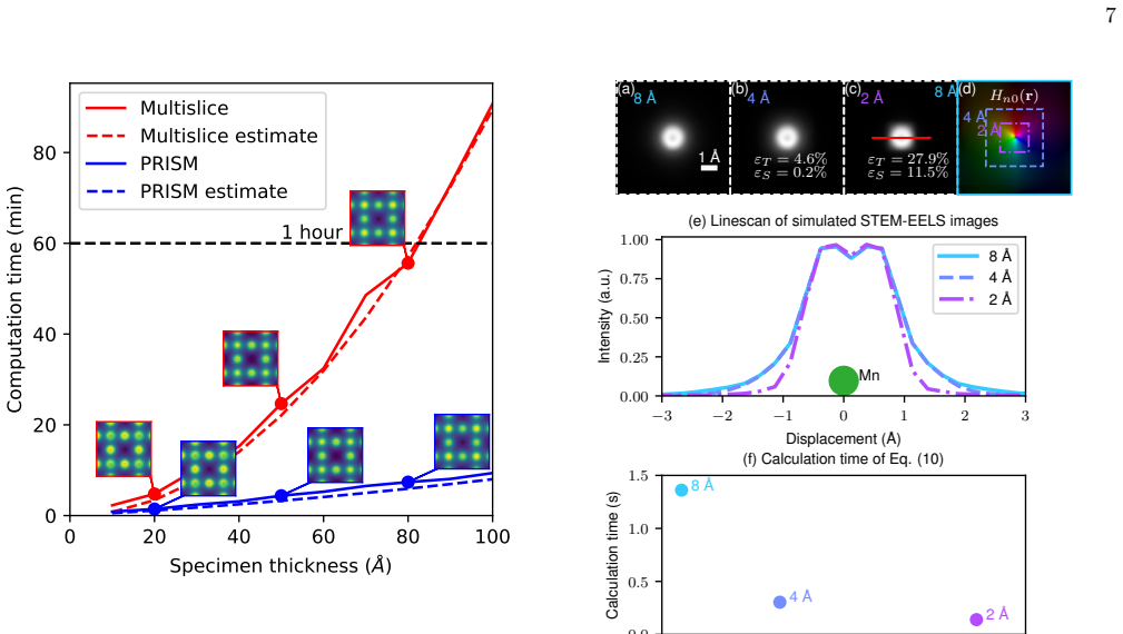
The central claim is that a STEM-EELS image can be written as $|S_n \psi_0|^2$ with $S_n = S_2 F H_{n0} F^{-1} S_1$, where $S_1$ is the scattering matrix from the probe-forming aperture to the plane of ionization, $H_{n0}$ is the ionization transition potential, and $S_2$ propagates the inelastically scattered wave to the EELS aperture. In the PRISM-EELS algorithm $S_1$ and $S_2$ are computed once per slice with multislice and then reused for every probe position, so the number of multislice iterations no longer grows with the size of the STEM raster. In a SrTiO3 comparison, the PRISM images agree with conventional multislice images to a normalized root-mean-square total error below 0.01% for thicknesses from 20 to 100 Å, while measured computation time grows roughly linearly with thickness rather than quadratically. For the FePt nanoparticle, a PRISM interpolation factor of 9, a cropped 4 Å transition grid, and the four dominant Fe L-edge transitions produce a 16-hour calculation; conventional multislice would take an estimated 87 days even with aggressive approximations, or 170 years without them.
Load-bearing premise
The method assumes that a forward multislice step can be reversed by applying the inverse of the slice transmission and propagation steps, but electrons scattered beyond the simulation grid's angular range are lost and cannot be recovered; for the strongly scattering FePt nanoparticle this inverse-multislice error was not checked against a full conventional simulation.
Editorial extensions
If this is right
- STEM-EELS simulations of nano-scale heterogeneous objects can be run routinely on desktop or GPU hardware in hours, making quantitative comparison with experimental elemental maps practical for nanoparticles, dopants, and interfaces.
- Because the multislice step is done once per slice rather than once per probe, adding scan positions or additional elemental edges to the same object becomes comparatively cheap.
- The cropped transition grid and inverse multislice approximations give users a controllable accuracy-speed trade-off, with roughly 1% error for a 16–24% speedup in the tested thickness range.
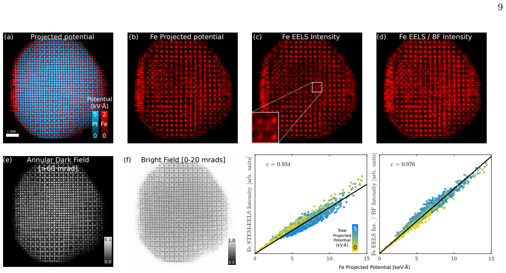
- The simulated FePt map reproduces the strong-scattering artifacts that complicate experimental EELS maps, and shows that dividing by a matched incoherent bright-field image raises the correlation between Fe density and EELS intensity from 0.935 to 0.976, offering a concrete correction recipe.
Reading between the lines
- The same two-scattering-matrix decomposition should transfer to other inelastic signals whose transition operators are multiplicative in real space, so the only element-specific input needed is the relevant transition potential.
- The inverse multislice operator is effectively a backpropagation through the specimen; its bandwidth-loss failure mode could be useful beyond EELS, for example in exit-wave reconstruction or ptychography where the same high-angle information is missing.
- The memory cost of storing the scattering matrices (about 4.4 GB for the 1836×1836 FePt example) sets a practical limit, so larger objects will likely require blockwise or streaming construction of $S_1$ and $S_2$.
- Because the headline calculation keeps only four of the Fe L-edge transitions and uses interpolation factor 9, a reproducibility test that recomputes the map with all transitions at $f=1$ on a smaller object would quantify the combined spatial error of those choices.
Signed reviews
Editorial analysis
A structured set of objections, weighed in public.
Referee Report
Summary. The paper extends the PRISM method to STEM-EELS simulation. Instead of propagating each inelastic wave separately for every scan position and transition, the algorithm stores two scattering matrices: S1 propagates the elastic probe to the plane of ionization and S2 propagates the inelastically scattered wave to the EELS detector. This reduces the number of multislice operations and changes the runtime scaling with specimen thickness from quadratic to approximately linear. Two further optimizations are presented: evaluating Eq. (11) on a cropped real-space grid around the transition site, and an "inverse multislice" operation (Eq. 19) that retreats S2 by one slice rather than recomputing it from the exit surface. The base PRISM method is validated against conventional multislice for SrTiO3 with total image errors below 0.01%, the inverse-multislice approximation gives errors around 1% for SrTiO3, and the cropping optimization has error/accuracy trade-offs quantified in Fig. 5. The paper closes with an 80 Å FePt nanoparticle EELS map computed in 16 hours, compared with an estimated 80 or more days for conventional multislice, and uses the map to demonstrate a bright-field-correction strategy for interpreting STEM-EELS images.
Significance. If the claims hold, this is a valuable contribution: it offers a concrete path to quantitative atomic-resolution STEM-EELS simulation for heterogeneous nanostructures that are currently too expensive to treat with conventional multislice methods. The paper's strengths include an explicit pseudocode description, measured FFT-based runtime models, validation against an independent conventional multislice implementation, and supplementary MATLAB code for the core algorithms. The quantitative error metrics in Figs. 4 and 6 and the falsifiable FePt demonstration are assets that go beyond a purely algorithmic proposal. The main weakness is that the linear-scaling inverse-multislice approximation is validated only on a relatively weak-scattering SrTiO3 specimen, while the headline FePt demonstration applies the same approximation to a strongly scattering 16,627-Pt-atom object without a reference calculation, leaving the dominant approximation error in the central demonstration unquantified.
major comments (3)
- [Sec. IV C and Sec. IV D, Eq. (19)] The inverse multislice approximation in Eq. (19) is the step that makes the algorithm's runtime scale linearly with thickness, but it is validated only on SrTiO3 in Fig. 6, where the errors are about 1% and the specimen is a relatively weak scatterer. The text itself notes that electrons scattered beyond the bandwidth limit are not recovered by the inverse operation. In the FePt demonstration of Sec. IV D, the same inverse operation is applied over 45 slices to an object containing 16,627 Pt atoms, which the paper identifies as producing strong high-angle scattering; no comparison is reported against either conventional multislice or PRISM without the inverse shortcut. As a result, the dominant approximation behind the headline 16-hour calculation has no quantified error bound for the object in which it is used.
- [Sec. IV D, Fig. 7] The FePt EELS map combines an interpolation factor of f=9, a 4 Å cropping window, and only four of the Fe L-edge transitions (about 90% of the signal), yet no reference calculation is provided for this object. Since the paper claims atomic-resolution quantitative maps and interprets the artifact morphology in Fig. 7(c), the combined spatial error of these approximations should be characterized, for example by comparing a cropped subvolume or a reduced scan against a full-multislice or at least an inverse-free PRISM calculation.
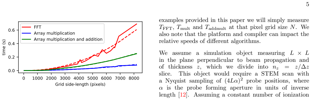
- [Sec. III, Eq. (17)] As printed, Eq. (17) does not contain any factor for the number of slices or inelastic transitions, so it does not by itself demonstrate the claimed linear scaling with nz; the text's argument that matrix multiplications dominate is plausible, but the missing sum or product over transitions should be written explicitly. The FePt runtime section reports an estimated runtime of 2 days from Eqs. (16) and (17) and an actual runtime of 16 hours without explaining the factor-of-three discrepancy; the runtime model would be more credible if this discrepancy were reconciled or the estimate revised.
minor comments (6)
- [Abstract and Sec. I] The phrase "for of a nanoparticle" should read "for a nanoparticle."
- [Sec. IV B / Fig. 5] The text refers to "11.4% as in Fig. 5(b)", but the caption lists 11.5% for panel (c); the cross-reference should be corrected.
- [Sec. IV B and Sec. IV D] "Energy loses" should be "energy losses" in the phrases "for energy loses 1 eV over the ionization threshold."
- [Eqs. (5) and (6)] The notation "z/n z" for the slice thickness is ambiguous; it should be written as z/n_z or Δz consistently.
- [Sec. IV A] The typo "In this sectio nwe" should be corrected to "In this section we."
- [Eq. (18)] The error metric should specify explicitly whether the site error εS uses the same normalization as the total error εT or a local normalization over the site window.
Circularity Check
No significant circularity: the algorithm is validated against an independent conventional multislice ground truth, and no fitted parameter is renamed as a prediction.
full rationale
The paper's central claim is that the PRISM-based STEM-EELS algorithm reproduces conventional multislice results while reducing computational cost. The validation in Sec. IV A directly compares PRISM-EELS images to conventional multislice images for the same SrTiO3 test case, reporting total errors below 0.01% (Fig. 4), and the inverse multislice approximation in Sec. IV C is likewise benchmarked against conventional multislice (Fig. 6). These are independent reference calculations, not outputs of the model being tested. The only fitted constants, A, B, and C in Sec. III, parameterize FFT and array-operation timings for runtime estimation; they do not enter the physics, the EELS intensities, or the error metrics. The FePt nanoparticle calculation in Sec. IV D is a demonstrated application of the method, and the absence of a full multislice reference for that specific object is a validation limitation rather than circular reasoning. The cited PRISM method (Ref. 14) is prior work by a co-author, but it is not used as the sole justification for correctness; the paper's own multislice comparisons supply independent support. No step reduces by construction to its inputs, no fitted parameter is presented as a prediction, and no load-bearing premise depends on an unverified self-citation. Thus the circularity score is 0.
Assumptions & free parameters
free parameters (4)
- Runtime scaling constants A, B, C =
A = 1.0e-9, B = 9.0e-9, C = 3.8e-9 (Matlab, this machine)
- PRISM interpolation factor f =
9 (nanoparticle calculation)
- Inelastic cropping window side length =
4 Å
- Number of Fe L-edge transitions included =
4 (just over 90% of total transitions)
assumptions (5)
- standard math The paraxial/small-angle Schrödinger equation (Eq. 1) governs fast-electron propagation through the specimen.
- domain assumption Multislice split-step approximation (Eq. 4) accurately solves Eq. (1) with thin slices.
- domain assumption Inelastic transition potential Hn0 from Saldin and Rez (Eq. 8-9) describes core-level ionization.
- standard math The transpose relation M^T (Eq. 14) correctly computes back-propagation for S2.
- domain assumption Inverse multislice M^-1 (Eq. 19) approximately inverts a forward iteration.
Cite this review
Pith. "Pith review of A linear-scaling algorithm for rapid computation of inelastic transitions in the presence of multiple electron scattering." pith.science (2026). https://pith.science/paper/G4INSSY7
@misc{pith2026190807628,
  author       = {Pith},
  title        = {Pith review of: A linear-scaling algorithm for rapid computation of inelastic transitions in the presence of multiple electron scattering},
  year         = {2026},
  howpublished = {\url{https://pith.science/paper/G4INSSY7}},
  note         = {Machine review of arXiv:1908.07628}
}
read the original abstract
Strong multiple scattering of the probe in scanning transmission electron microscopy (STEM) means image simulations are usually required for quantitative interpretation and analysis of elemental maps produced by electron energy-loss spectroscopy (EELS). These simulations require a full quantum-mechanical treatment of multiple scattering of the electron beam, both before and after a core-level inelastic transition. Current algorithms scale quadratically and can take up to a week to calculate on desktop machines even for simple crystal unit cells and do not scale well to the nano-scale heterogeneous systems that are often of interest to materials science researchers. We introduce an algorithm with linear scaling that typically results in an order of magnitude reduction in compute time for these calculations without introducing additional error and discuss approximations that further improve computational scaling for larger scale objects with modest penalties in calculation error. We demonstrate these speed-ups by calculating the atomic resolution STEM-EELS map using the L-edge transition of Fe, for of a nanoparticle 80 \AA\ in diameter in 16 hours, a calculation that would have taken at least 80 days using a conventional multislice approach.
Figures

Figures from the paper (2 more)

Reference graph
Works this paper leans on
-
[1]
H. L. Xin, J. A. Mundy, Z. Liu, R. Cabezas, R. Hovden, L. F. Kourkoutis, J. Zhang, N. P. Subramanian, R. Makharia, F. T. Wagner, et al. , Atomic-resolution spectroscopic imaging of ensembles of nanocatalyst particles across the life of a fuel cell, Nano letters 12, 490 (2011)
work page 2011
-
[2]
J. A. Mundy, Q. Mao, C. M. Brooks, D. G. Schlom, and D. A. Muller, Atomic-resolution chemical imaging of oxygen local bonding environments by electron energy loss spectroscopy, Applied Physics Letters 101, 042907 (2012)
work page 2012
-
[3]
J. A. Mundy, Y. Hikita, T. Hidaka, T. Yajima, T. Higuchi, H. Y. Hwang, D. A. Muller, and L. F. Kourkoutis, Visualizing the interfacial evolution from charge compensation to metallic screening across the manganite metal–insulator transition, Nature communications 5, 3464 (2014)
work page 2014
-
[4]
R. R. Zamani, F. S. Hage, S. Lehmann, Q. M. Ramasse, and K. A. Dick, Atomic-resolution spectrum imaging of semiconductor nanowires, Nano letters 18, 1557 (2017)
work page 2017
-
[5]
R. F. Egerton, Electron energy-loss spectroscopy in the electron microscope (Springer Science & Business Media, 2011)
work page 2011
-
[6]
D. A. Muller, Y. Tzou, R. Raj, and J. Silcox, Mapping sp2 and sp 3 states of carbon at sub-nanometre spatial resolution, Nature 366, 725 (1993)
work page 1993
-
[7]
D. A. Muller, L. F. Kourkoutis, M. Murfitt, J. Song, H. Hwang, J. Silcox, N. Dellby, and O. Krivanek, Atomic- scale chemical imaging of composition and bonding by aberration-corrected microscopy, Science 319, 1073 (2008)
work page 2008
- [8]
Show all 26 references
-
[9]
L. J. Allen, D. C. Bell, T. W. Josefsson, A. E. C. Spargo, and S. L. Dudarev, Inner-shell ionization cross sections and aperture size in electron energy-loss spectroscopy, Physical Review B 56, 9 (1997)
1997
-
[10]
L. J. Allen, S. D. Findlay, et al. , Modelling the inelastic scattering of fast electrons, Ultramicroscopy 151, 11 (2015)
2015
-
[11]
Lobato, S
I. Lobato, S. Van Aert, and J. Verbeeck, Progress and new advances in simulating electron microscopy datasets using MULTEM, Ultramicroscopy 168, 17 (2016)
2016
-
[12]
Dwyer, Simulation of scanning transmission electron microscope images on desktop computers, Ultramicroscopy 110, 195 (2010)
C. Dwyer, Simulation of scanning transmission electron microscope images on desktop computers, Ultramicroscopy 110, 195 (2010)
2010
-
[13]
Dwyer, The role of symmetry in the theory of inelastic high-energy electron scattering and its application to atomic-resolution core-loss imaging, Ultramicroscopy 151, 68 (2015)
C. Dwyer, The role of symmetry in the theory of inelastic high-energy electron scattering and its application to atomic-resolution core-loss imaging, Ultramicroscopy 151, 68 (2015)
2015
-
[14]
Ophus, A fast image simulation algorithm for scanning transmission electron microscopy, Advanced structural and chemical imaging 3, 13 (2017)
C. Ophus, A fast image simulation algorithm for scanning transmission electron microscopy, Advanced structural and chemical imaging 3, 13 (2017)
2017
-
[15]
Pryor, C
A. Pryor, C. Ophus, and J. Miao, A streaming multi- GPU implementation of image simulation algorithms for scanning transmission electron microscopy, Advanced structural and chemical imaging 3, 15 (2017)
2017
-
[16]
Yang, C.-C
Y. Yang, C.-C. Chen, M. C. Scott, C. Ophus, R. Xu, A. Pryor, L. Wu, F. Sun, W. Theis, J. Zhou, et al. , Deciphering chemical order/disorder and material properties at the single-atom level, Nature 542, 75 (2017)
2017
-
[17]
Van Dyck, Image calculations in high-resolution electron microscopy: problems, progress, and prospects, in Advances in electronics and electron physics , Vol
D. Van Dyck, Image calculations in high-resolution electron microscopy: problems, progress, and prospects, in Advances in electronics and electron physics , Vol. 65 (Elsevier, 1985) pp. 295–355
1985
-
[18]
E. J. Kirkland, Advanced computing in electron microscopy (Springer Science & Business Media, 2010)
2010
-
[19]
Bethe, Theorie der beugung von elektronen an kristallen, Annalen der Physik 392, 55 (1928)
H. Bethe, Theorie der beugung von elektronen an kristallen, Annalen der Physik 392, 55 (1928)
1928
-
[20]
C. J. Humphreys, The scattering of fast electrons by crystals, Reports on Progress in Physics 42, 1826 (1979)
1979
-
[21]
We use the following convention, a forward Fourier transform is given by ˆψ(g) = ˆFr→gψ(r) =∫ ψ(r)e−2πir·gdr and an inverse Fourier transform is given by ψ(r) = ˆF−1 g→r ˆψ(r) = ∫ ˆψ(g)e2πir·gdr
-
[22]
S. D. Findlay, L. J. Allen, M. P. Oxley, and C. J. Rossouw, Lattice-resolution contrast from a focused coherent electron probe. part II, Ultramicroscopy 96, 65 (2003)
2003
-
[23]
D. K. Saldin and P. Rez, The theory of the excitation of atomic inner-shells in crystals by fast electrons, Philosophical Magazine B 55, 481 (1987)
1987
-
[24]
M. P. Oxley and L. J. Allen, Delocalization of the effective interaction for inner-shell ionization in crystals, Physical Review B 57, 3273 (1998)
1998
-
[25]
Y. Zhu, A. Soukiassian, D. G. Schlom, D. A. Muller, and C. Dwyer, Towards artifact-free atomic- resolution elemental mapping with electron energy- loss spectroscopy, Applied Physics Letters 103, 141908 (2013)
2013
-
[26]
A full multislice calculation without these additional approximations is estimated to take 170 years for one frozen phonon pass
Reviewed August 14, 2026 · model on record in the stance chip above.
Discussion (0). Continue with ORCID to comment.