REVIEW 4 major objections 4 minor 28 references
Optimized Bistable Vortex Memory Arrays for Superconducting In-Memory Matrix-Vector Multiplication
T0 review · 4 major / 4 minor · reviewed 2026-08-06 · deepseek-v4-flash
Pith's one-line read Bistable vortex memory arrays can multiply in memory by converting summed read currents into pulse counts, the paper argues.
desk verdict A clever BVM+QB+T1 in-memory multiplier that is plausible in simulation, but the headline latency is internally inconsistent and the pulse-count linearity is verified in only one ideal case. read the letter →
The pith
A machine-rendered reading of the paper's core claim, the machinery that carries it, and where it could break.
The reading
What carries the argument
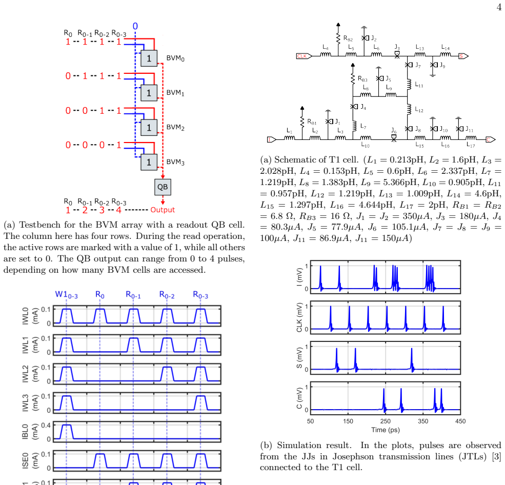
The load-bearing object is the BVM read path: a storage loop with two vortex circulation states, a readout loop, and a sense line shared by a column. During a read, the sense current from every selected cell storing 1 adds linearly, and the QB cell, a thresholded buffer, converts the combined amplitude into a variable number of SFQ pulses. T1 cells are synchronous-sum/asynchronous-carry binary adder cells that consume the pulse trains; the number of pulses on a column is the binary weight of that column's partial product, so counting and carry propagation complete the multiply. The optimized direct-input variant changes the array wiring: sense lines are connected diagonally and the memory is uniformly preloaded with 1s, eliminating 12 cells and three bit lines and letting both operands be streamed in as inputs.
What would settle it
Read a single BVM column of four cells, all storing 1, many times while sweeping the QB threshold within the reported margins and across process-variation samples; if any valid setting yields a pulse count other than four for four ones, the current-summation premise fails. Equivalently, a dc measurement of sense-line current versus number of simultaneously read rows must be a straight line through the origin with zero row-to-row crosstalk.
Extended reading notes
Core claim
The central discovery is that the BVM cell's read current can be made to do the partial-product accumulation of binary multiplication. In the proposed 4x4 multiplier, one operand is stored as vortex patterns in the array (or, in the optimized version, all cells are preloaded with 1s and both operands are applied as row and column inputs); when the rows selected by a 1 bit are read, the sense line for each column carries a current proportional to the number of ones in that column. The Quantizer Buffer is biased so that each unit of current emits exactly one SFQ pulse, producing a pulse train whose length equals the column count, and T1 cells with asynchronous carry output add these pulse trains and propagate the carry once to produce the product with a single clock. The paper validates this with a 4-bit example (11 times 13 yields 143) and an MVM example, and reports the multiplier operating at 20 GHz with 50 ps latency using about 550 Josephson junctions against about 13,117 for a conventional synthesized 4-bit SFQ multiplier.
Load-bearing premise
The design assumes that when several BVM cells storing 1 are read at once, the current summed on the shared sense line is exactly proportional to the number of ones and that the Quantizer Buffer threshold can be fixed so every unit of current produces exactly one SFQ pulse; this linear pulse-code is checked in one noise-free simulation and any threshold drift, inductance mismatch, or process variation would corrupt the product.
Editorial extensions
If this is right
- A 4-bit BVM multiplier runs at 20 GHz with 50 ps latency in simulation, versus 270 ps for the conventional 44.4 GHz SFQ multiplier used as baseline, and uses about 550 instead of 13,117 Josephson junctions.
- The optimized direct-input array requires only one initialization cycle because all cells are preloaded with 1s; thereafter both operands are applied as active read and column inputs, so repeated multiplication avoids memory rewrites.
- Adding T1 cells and D flip-flops at the output extends the multiplier to multiply-accumulate, retaining the carry across accumulation cycles and supporting 15-bit accumulation with a dedicated intermediate clock.
- Tiling the single-cycle multipliers in a systolic array computes each element of a matrix-vector product in four clock cycles at 20 GHz in simulation, and the same tiling extends to matrix-matrix multiplication.
- Because only standard Josephson junctions are used, the design is compatible with conventional superconducting fabrication processes and does not rely on ferromagnetic or exotic junctions.
Reading between the lines
- This reader's inference: the pulse-count linearity assumption sets an upper bound on array width; at some column size the accumulated current will exceed the Quantizer Buffer's linear range, so scaling to larger matrices likely requires segmented sense lines or multiple QB thresholds.
- This reader's inference: a direct test for hardware is to read the same column repeatedly and histogram QB pulse counts; the spread of that histogram across process corners is the yield metric that decides whether the approach survives fabrication.
- This reader's inference: because the carry propagates once asynchronously, the multiplier latency should grow with operand width roughly linearly; a 16-bit version could be benchmarked by simulation before fabrication to test whether the 50 ps figure scales.
- This reader's inference: signed arithmetic is not addressed; encoding operands in offset binary (adding a constant current pedestal and subtracting it after quantization) would extend the same BVM crossbar to signed neural-network weights.
Signed reviews
Editorial analysis
A structured set of objections, weighed in public.
Referee Report
Summary. The paper proposes a superconducting in-memory multiplier and matrix-vector multiplication (MVM) architecture built from Bistable Vortex Memory (BVM) cells, Quantizer Buffers (QBs), and T1 adder cells. BVM cells store bits nonvolatily; when several cells in a column are read simultaneously, their sense-line currents are assumed to add linearly, and the QB converts the summed current into a variable number of SFQ pulses equal to the number of stored ones. These pulses feed T1 adders that perform binary addition and carry propagation, producing the product in one clock cycle. The authors present a 4-bit multiplier example (11 × 13 = 143), an optimized diagonal sense-line layout intended to save area, a MAC extension, and a systolic tiled MVM architecture. Simulations with JoSIM are used to validate the components and the 11 × 13 multiplication, and the paper claims 20 GHz operation, 50 ps multiplier latency, and roughly 20 times fewer Josephson junctions than a conventional SFQ multiplier.
Significance. If the central pulse-count linearity assumption is correct, the architecture is an interesting integration of nonvolatile superconducting memory with arithmetic, potentially reducing area and power relative to conventional SFQ multipliers while avoiding exotic materials. The paper's strengths are its use of standard Josephson junctions, the concrete 11 × 13 simulation, the explicit comparison with a ColdFlux-synthesized multiplier, and the extension to MVM and MAC operations. However, the current evidence is based on ideal, noise-free simulations of a single multiplication and one row of an MVM; the basic working of the multiplier is demonstrated, but the load-bearing mechanism that a QB emits exactly one pulse per stored one is not yet established with sufficient margin or pattern coverage. The performance claims also contain internal inconsistencies that must be resolved.
major comments (4)
- [Sec. 2.2, Fig. 2] The paper's central mechanism is that when multiple BVM cells are read simultaneously, the QB emits a number of SFQ pulses exactly equal to the number of stored ones, and this is the basis for the entire multiplier and MVM. The only evidence provided is a testbench in which all cells store 1 and rows are read one at a time, plus the single 11 × 13 example in Fig. 5. No simulation with mixed 0/1 patterns, no column with two or four simultaneously read stored ones, and no sensitivity study of the QB threshold or sense-line inductance is reported. Since the T1 adder stage and the final product are correct only if the pulse count equals the column sum, this missing validation is load-bearing. Please add simulations with mixed data patterns and a parameter sweep (QB threshold, sense-line inductance, JJ critical-current spread) to demonstrate that the pulse-count linearity is robust.
- [Sec. 3.1, Fig. 6] The optimized direct-input BVM array is described as eliminating 12 BVM cells and three bit lines, but it is never simulated. The simulation results presented in Figs. 4, 5, and 9 correspond to the preload configuration, not to the direct-input configuration of Fig. 6. The claim that preloading all cells with 1 and applying inputs through SE and BL implements an AND mask and preserves correct current summation needs direct simulation evidence, including the effect of the diagonal sense-line connections on timing and accumulation. Without this, the area and initialization-cycle improvements are not substantiated.
- [Sec. 3, Fig. 5b] The stated performance of 20 GHz with 50 ps latency appears inconsistent with the simulation description. The text says that QB pulses appear before 70 ps and that carry propagation occurs between 70 and 100 ps, after which a clock pulse latches the product. If latency is measured from input arrival to output, the observed latency is greater than 100 ps; if it is measured from the final clock edge, that definition should be stated explicitly. Please provide the actual simulation timing diagram with input arrival, clock edges, and output valid times, and reconcile the 50 ps claim with the 20 GHz clock period.
- [Sec. 4, Fig. 9] The MVM demonstration covers only the first row of the 4 × 4 matrix (y1 = 546); the remaining three output elements are not simulated. The abstract and Sec. 4 claim that an MVM structure operates at 20 GHz, which overstates the evidence. Please either simulate a full 4 × 4 MVM tile (or at least a second row) explicitly, or revise the claim to state that only the first row was verified. In addition, the synchronization scheme for the tiled multipliers (input delays, per-PE clocks, and reconfiguration for arbitrary matrices) is only described qualitatively and should be specified in enough detail to reproduce the claimed 20 GHz operation.
minor comments (4)
- [Abstract and Sec. 1] The abstract states a 4-bit multiplier with 50 ps latency, while the introduction states a throughput of 20 GHz and a latency of 200 ps. These two latency figures should be reconciled.
- [Fig. 3 caption] The caption lists J11 = 86.9 µA and then J11 = 150 µA; one of these should presumably be J12 or another device label. Also, 'J4 = 80 .3µA' has an extra space.
- [Sec. 4, Eq. 3] The text refers to 'In Eq. 3', but the displayed equation is not actually numbered in the manuscript. Please number the equation or revise the cross-reference.
- [Sec. 3.2] The notation 'T16−0' and 'T113−7' is ambiguous; using subscripts or a clearer range notation such as T1_6 to T1_0 would improve readability.
Circularity Check
No significant circularity: the multiplier is an integrated design validated against independent arithmetic, not a derivation that consumes its own inputs.
full rationale
The paper's claimed derivation chain is a circuit integration, not a mathematical derivation. The BVM cell [25], Quantizer Buffer [28], and T1 cell [26] are prior-published components; the two former are same-group self-citations, but they are used as device models with stated behavior published before this paper's target result, so they are independent support rather than circular premises. The central mechanism (current accumulates on the shared sense line, and the QB emits a pulse count matching the number of stored 1s) is an explicit physical assumption verified by a JoSIM testbench, not an equation that defines the output as the input. The QB threshold is a circuit bias setting tuned so one cell produces one pulse; this is calibration of a design, not a fitted parameter renamed as a 'prediction' of an independent quantity. Arithmetic validation checks the full circuit against known values (11×13=143; Eq. (3) row results), so the design is self-contained against external truth. The only concerns—unverified linearity under mixed 0/1 patterns, lack of margin analysis, and an apparent timing inconsistency between the claimed 50 ps latency and the 70–100 ps carry propagation in Fig. 5(b)—are correctness and robustness risks, not circularity.
Assumptions & free parameters
free parameters (4)
- QB threshold current =
set to the output level of a single BVM cell (not quantified)
- Operating clock frequency =
20 GHz
- Input delay matching in MVM =
not specified
- JTL delay matching for first column =
not specified
assumptions (5)
- standard math Binary arithmetic with carry propagation (used in T1 adder cells)
- domain assumption BVM cell behaves as described in [25] (vortex state readout via SE/SL)
- domain assumption T1 cell behaves as described in [26] (synchronous sum, asynchronous carry)
- domain assumption QB cell produces a pulse count proportional to input current
- ad hoc to paper Current summation on a shared sense line is linear and simultaneous
Cite this review
Pith. "Pith review of Optimized Bistable Vortex Memory Arrays for Superconducting In-Memory Matrix-Vector Multiplication." pith.science (2026). https://pith.science/paper/HI2PP46K
@misc{pith2026250704648,
  author       = {Pith},
  title        = {Pith review of: Optimized Bistable Vortex Memory Arrays for Superconducting In-Memory Matrix-Vector Multiplication},
  year         = {2026},
  howpublished = {\url{https://pith.science/paper/HI2PP46K}},
  note         = {Machine review of arXiv:2507.04648}
}
read the original abstract
Building upon previously introduced Bistable Vortex Memory (BVM) as a novel, nonvolatile, high-density, and scalable superconductor memory technology, this work presents a methodology that uses BVM arrays to address challenges in data-driven algorithms and neural networks, specifically focusing on matrix-vector multiplication (MVM). The BVM approach introduces a novel superconductor-based methodology for in-memory arithmetic, achieving ultra-high-speed and energy-efficient computation by utilizing BVM arrays for in-memory computation. The design employs a tiled multiplier structure where BVM's inherent current summation capability is combined with Quantizer Buffer (QB) cells to convert the analog accumulated current into a variable number of digital Single Flux Quantum (SFQ) pulses. These pulses are then processed by T1 adder cells, which handle binary addition and carry propagation, thereby forming a complete functional multiplier unit. This paper thus presents an efficient MVM architecture that uses these BVM-based multipliers in a systolic array configuration to enable parallel computation. A key innovation is an optimized BVM array structure specifically tailored for multiplication applications, involving a restructuring of Sense Lines (SLs) with diagonal connections to reduce area and an adjusted input scheme to enhance computational efficiency compared to the general-purpose BVM array design. We demonstrate the efficacy of this approach with a 4-bit multiplier operating at 20 GHz with 50 ps latency and an MVM structure demonstrating operation at 20 GHz. Furthermore, we showcase how this multiplier design can be extended to support Multiply-Accumulate (MAC) operations. This work paves the way for power-efficient neural networks by enabling high-speed in-memory computation.
Figures


Figures from the paper (5 more)


Reference graph
Works this paper leans on
-
[1]
Holmes D S 2021 Cryogenic electronics and quantum in- formation processing 2021 IEEE International Roadmap for Devices and Systems Outbriefs(IEEE) pp 1–93
work page 2021
-
[2]
Razmkhah, Sasan and Febvre, Pascal 2023 Superconducting Quantum Electronics Beyond-CMOS (ISTE & WILEY) chap 8, pp 295–391 ISBN 9781394228713
work page 2023
-
[3]
Likharev K K and Semenov V K 1991 IEEE transactions on applied superconductivity1 3–28
work page 1991
-
[4]
Takeuchi N, Ozawa D, Yamanashi Y and Yoshikawa N 2013 Superconductor Science and Technology26 035010
work page 2013
-
[5]
Razmkhah S, Aviles R S, Li M, Gupta S, Beerel P A and Pedram M 2024 Challenges and unexplored frontiers in electronic design automation for superconducting digital logic 2024 Design, Automation & Test in Europe Conference & Exhibition (DATE)(IEEE) pp 1–6
work page 2024
-
[6]
Cong H, Li M and Pedram M 2021 IEEE Transactions on Applied Superconductivity31 1–10
work page 2021
-
[7]
Nagaoka I, Ishida K, Tanaka M, Sano K, Yamashita T, Ono T, Inoue K and Fujimaki A 2021 IEEE Transactions on Applied Superconductivity31 1–5
work page 2021
-
[8]
Yamanashi Y, Okumura H and Yoshikawa N 2024 Superconductor Science and Technology37 115024
work page 2024
Show all 28 references
-
[9]
2023 IEEE Transactions on Applied Superconductivity 33 1–26
Fourie C J, Jackman K, Delport J, Schindler L, Hall T, Febvre P, Iwanikow L, Chen O, Ayala C L, Yoshikawa N et al. 2023 IEEE Transactions on Applied Superconductivity 33 1–26
2023
-
[10]
McCanny J and McWhirter J 1983 IEE Proceedings G (Electronic Circuits and Systems)130(4) 125–130
1983
-
[11]
Alam S, Hutchins J, Hossain M S, Ni K, Narayanan V and Aziz A 2023 Cryogenic in-memory matrix-vector mul- tiplication using ferroelectric superconducting quantum interference device (fe-squid) 2023 60th ACM/IEEE De- sign Automation Conference (DAC)pp 1–6
2023
-
[12]
Zolfagharinejad M, Alegre-Ibarra U, Chen T, Kinge S and van der Wiel W G 2024 The European Physical Journal B 97 70
2024
-
[13]
Bao H, Zhou H, Li J, Pei H, Tian J, Yang L, Ren S, Tong S, Li Y, He Y et al.2022 Frontiers of Optoelectronics15 23
2022
-
[14]
Siegl P, Buchty R and Berekovic M 2016 Data-centric computing frontiers: A survey on processing-in-memory Proceedings of the Second International Symposium on Memory Systems pp 295–308
2016
-
[15]
Seshadri V, Lee D, Mullins T, Hassan H, Boroumand A, Kim J, Kozuch M A, Mutlu O, Gibbons P B and Mowry T C 2017 Ambit: In-memory accelerator for bulk bitwise operations using commodity dram technology Proceedings of the 50th Annual IEEE/ACM International Symposium on Microarch...
2017
-
[16]
org/document/1083337/
Chua L 1971 IEEE Transactions on Circuit Theory18 507– 519 ISSN 0018-9324 URL http://ieeexplore.ieee. org/document/1083337/
1971
-
[17]
Strukov D B, Snider G S, Stewart D R and Williams R S 2008 nature 453 80–83
2008
-
[18]
Williams R S 2008 IEEE spectrum 45 28–35
2008
-
[19]
Sun W, Gao B, Chi M, Xia Q, Yang J J, Qian H and Wu H 2019 Nature communications10 3453
2019
-
[20]
Zidan M A, Strachan J P and Lu W D 2018 Nature electronics 1 22–29
2018
-
[21]
Lee J and Lu W D 2018 Advanced Materials30 1702770
2018
-
[22]
Yao P, Wu H, Gao B, Tang J, Zhang Q, Zhang W, Yang J J and Qian H 2020 Nature 577 641–646
2020
-
[23]
Han Y, Nickle C, Zhang Z, Astier H P, Duffin T J, Qi D, Wang Z, Del Barco E, Thompson D and Nijhuis C A 2020 Nature materials 19 843–848
2020
-
[24]
Jung S, Lee H, Myung S, Kim H, Yoon S K, Kwon S W, Ju Y, Kim M, Yi W, Han S et al.2022 Nature 601 211–216
2022
-
[25]
Karamuftuoglu M, Ucpinar B, Razmkhah S and Pedram M 2024 Superconductor Science and Technology38 015020
2024
-
[26]
Bairamkulov R, Yu M and De Micheli G 2024 Unleashing the Power of T1-cells in SFQ Arithmetic Circuits Proceedings of the 61st ACM/IEEE Design Automation Conference pp 1–6
2024
-
[27]
Delport J A, Jackman K, Le Roux P and Fourie C J 2019 IEEE Transactions on Applied Superconductivity29 1–5
2019
-
[28]
Razmkhah S, Karamuftuoglu M A and Bozbey A 2024 Superconductor Science and Technology37 065011
2024
Reviewed August 6, 2026 · model on record in the stance chip above.
Discussion (0). Continue with ORCID to comment.