REVIEW 3 major objections 5 minor 173 references
Graphene Electro-Absorption Modulators for Energy-Efficient and High-Speed Optical Transceivers
T0 review · 3 major / 5 minor · reviewed 2026-08-07 · deepseek-v4-flash
Pith's one-line read Graphene electro-absorption modulators hit 80 Gbit/s at 58 fJ/bit.
desk verdict Record bandwidth for graphene EAMs is credible, but the 58fJ/bit energy claim is off by a factor of ~4 and the 80Gbit/s BER is above FEC limits. read the letter →
The pith
A machine-rendered reading of the paper's core claim, the machinery that carries it, and where it could break.
The reading
What carries the argument
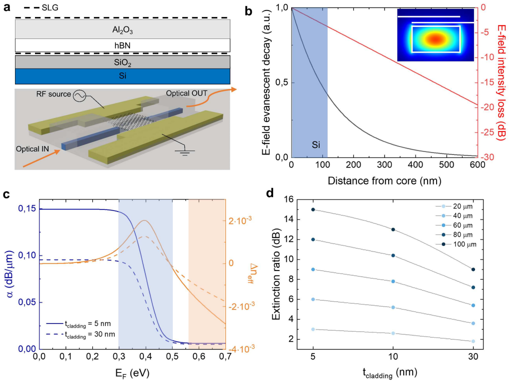
The central object is the double single-layer graphene electro-absorption modulator (DSLG EAM): a SLG/dielectric/SLG capacitor placed on a thin oxide cladding above a silicon waveguide, with 3.5nm hBN plus PE-ALD Al2O3 as the gate dielectric. The operating mechanism is Pauli blocking: gating moves the graphene Fermi level, turning interband absorption on or off, which changes the mode's extinction coefficient; simulations use a graphene surface-conductivity model with $\tau=350$fs, matching the measured $\mu\sim8000$cm$^2$/Vs. The bandwidth claim is carried by a lumped-element RC model, $V_C/V_T=1/(1+i\omega R_T C_T)$, where $C_T$ is the series combination of oxide capacitance $C_{\text{ox}}$ and graphene quantum capacitance $C_Q$, and $R_T$ includes contact, gated, and ungated graphene resistances. This model predicts 70GHz for the 40nm-oxide, 40µm device, close to the measured 67GHz. The energy claim uses $E_{\text{bit}}=CV_{\text{pp}}^2/4$, and the fabrication process is carried by selective CMP/dry-etch planarization that limits SLG to active sections plus two-step Au metallization that reduces contact resistance.
What would settle it
Measure the low-frequency capacitance of the finished 40nm-oxide modulator as a function of bias using an $S_{11}$ measurement, record the actual peak-to-peak voltage at the probe tip during 80Gbit/s transmission, and compute $E_{\text{bit}}=CV_{\text{pp}}^2/4$; if the result exceeds 58fJ/bit by several times, the headline energy claim is not supported.
Extended reading notes
Core claim
The claim is that voltage applied across two CVD graphene sheets separated by an hBN/Al2O3 dielectric shifts the Fermi level of both sheets, switching their interband absorption through Pauli blocking and modulating light carried in the silicon waveguide's evanescent field. For the 40nm-oxide, 40µm-long design, the authors measure a 3dB electro-optic bandwidth of 67GHz and NRZ eye diagrams at 60 and 80Gbit/s in the C band, with 40Gbit/s demonstrated in the O band. They report static extinction ratios up to ~4.5dB, average ER ~0.12dB/µm for the 20nm-oxide design, modulation efficiency ~0.037dB/Vµm, insertion loss ~0.9dB, and a dynamic energy estimate of ~58fJ/bit from $E_{\text{bit}}=CV_{\text{pp}}^2/4$. The paper concludes that wafer-scale graphene amplitude modulators can now deliver the speed and energy budget needed for Tbit/s, DSP-free NRZ transceivers in data-centre and AI optical networks.
Load-bearing premise
The 58fJ/bit energy figure assumes that the capacitance entering $E_{\text{bit}}=CV_{\text{pp}}^2/4$ is the small effective value the estimate requires, but the paper does not report a direct measurement of that capacitance or of the voltage actually reaching the modulator.
Editorial extensions
If this is right
- At 80Gbit/s per lane, 20 modulators on one photonic circuit would form a 1.6Tbit/s transmitter, the configuration the paper proposes for DSP-free NRZ links.
- Because the same devices operate in the O and C bands, one platform can serve intra-data-centre interconnects at 1.3µm and longer-reach C-band links at 1.55µm without a material change.
- At ~58fJ/bit and ~0.9dB insertion loss, the modulator sits below the 100fJ/bit component budget the paper identifies as necessary for sub-pJ/bit transceivers.
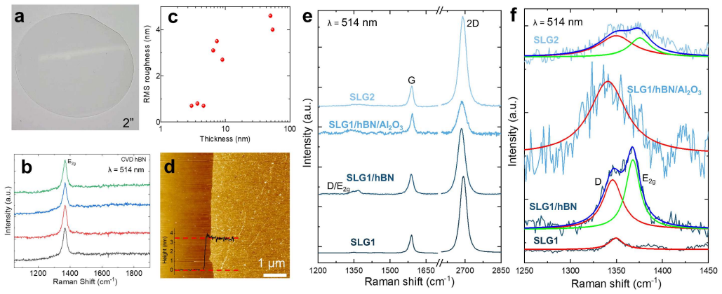
- The fabrication flow uses CVD graphene, MOCVD hBN, and 200mm SOI processing, which is compatible with foundry multi-project-wafer runs rather than only bespoke lab fabrication.
Reading between the lines
- An implication the authors leave implicit is that the 58fJ/bit number depends on an effective capacitance that is never directly reported; the geometric capacitance of a 40nm oxide over the 22µm2 active area at the stated ~7V drive would give roughly 370fJ/bit, so either the effective capacitance or the actual on-device voltage swing must be much smaller than the nominal values.
- A consequence not stated in the paper is that the measured BER at 80Gbit/s, ~8.5e-3, is far above the 1e-12 typically required for FEC-free links, so the DSP-free transceiver vision still depends on receiver improvements or coding despite the modulator's bandwidth.
- A testable extension would be a low-frequency $S_{11}$ capacitance-voltage measurement on the finished devices, which would convert the energy-per-bit estimate from an assumption into a measured quantity.
- The paper's own circuit model predicts that reducing post-transfer doping and contact resistance could push the same design toward ~90GHz, making post-transfer doping control the clearest experimental lever for the next generation.
Editorial analysis
A structured set of objections, weighed in public.
Referee Report
Summary. The paper reports double-single-layer-graphene electro-absorption modulators fabricated with a wafer-scalable process on 200 mm SOI, claiming a 67 GHz electro-optic bandwidth, 80 Gbit/s NRZ data transmission in the C-band and 40 Gbit/s in the O-band, a dynamic energy consumption of about 58 fJ/bit, a modulation efficiency of about 0.037 dB/V·µm, and low insertion loss. The device design is supported by an RC circuit model whose inputs are independently measured mobility, contact resistance, and dielectric permittivity, and the static extinction-ratio and S21 measurements are reported in detail.
Significance. If the headline claims hold, this is a substantial advance for graphene-based silicon photonic modulators: wafer-scale integration of CVD graphene, a directly measured 67 GHz electro-optic bandwidth, and a modulation efficiency of 0.037 dB/V·µm on par with the best exfoliated-graphene devices. The RC model is a strength because it uses independently characterized transport and dielectric parameters rather than fitting the measured bandwidth. The two load-bearing weaknesses are the unsubstantiated 58 fJ/bit energy claim and the high bit-error-rate at the advertised 80 Gbit/s data rate; both affect the central 'fastest and most efficient' conclusion.
major comments (3)
- [Table I and 'Dynamic characterization'] The energy-per-bit values in Table I are not supported by the reported device parameters. For the 40 nm-gate-oxide device, the stated active area of 22 µm², the measured relative permittivity of about 6.9, and the stated drive condition Vpp≈7 V imply a geometric capacitance of about 34 fF and hence CVpp²/4 ≈ 410 fJ/bit, not 58 fJ/bit. The manuscript does not report the effective capacitance C used in the E_bit=CVpp²/4 formula, nor the actual peak-to-peak voltage delivered to the modulator as opposed to the DAC output. The same issue affects the 20 nm-oxide device (26 fJ/bit with a 13 µm² area implies Vpp≈1.6 V, while the DC sweep in Fig. 8a uses about 10 V). Please report the measured modulator capacitance and the on-device voltage swing, or revise the energy claims and the '~3x lower energy' comparison.
- [Table IV and 'Bandwidth and data transmission'] The headline '80Gbit/s NRZ data rate' is based on a filtered BER of 8.5×10^-3 for the 40 µm modulator, which is above typical FEC thresholds (for example, KP4-FEC pre-FEC BER is about 2.4×10^-4, and even HD-FEC is about 3.8×10^-3). With this BER, the 80 Gbit/s link is not error-free under standard forward error correction. The paper should state the BER threshold assumed and either demonstrate a lower BER with a defined FEC or qualify the data-rate claim accordingly.
- [Abstract and 'Graphene integration' / Table I] The abstract claims '~0.037dB/Vµm modulation efficiency, ~16 times better than previous demonstrations based on graphene', but the text (Section 'Graphene integration' and Table I) states that the same value of 0.037 dB/V·µm was already reported for exfoliated-graphene/hBN devices in Ref. [76]. The 16× improvement applies only to the CVD-graphene modulator of Ref. [75]. Please specify the comparator explicitly in the abstract and in the main text.
minor comments (5)
- [Table I] The table header lists 'CVpp²/4 [fJ/bit]' but the table does not report C or Vpp for any device; adding these columns would make the energy comparison reproducible and would directly address the energy-claim issue.
- [Abstract and 'Bandwidth and data transmission'] The claim of 'operation in both O and C bands' is correct, but the O-band demonstration is limited to 40 Gbit/s while the C-band demonstration reaches 80 Gbit/s; please state this asymmetry explicitly in the abstract or conclusions.
- [Eq. (3)] In the Kubo-formula expression, the denominator of the second term contains '(ω − 12Γ)2', which appears to be a typographical error for '(ω − i2Γ)2' or a missing imaginary unit; please correct and check the notation.
- [Fig. 9b and 'Bandwidth and data transmission'] The S21 curve is extrapolated from -55.5 to -58.5 dB to determine f3dB=67 GHz; please state the fitting range, the uncertainty of the extrapolation, and how the photodiode and probe responses were subtracted.
- [Dynamic characterization set-up] There are typographical errors in the setup description: 'groud-signal' should be 'ground-signal' and 'Porbe' should be 'Probe'.
Circularity Check
No significant circularity: the EO-BW and ER simulations use independently measured parameters and are validated against measured data; the energy claim is under-reported but not a circular step.
full rationale
The paper's central derivation chain is self-contained and not circular. The EO-BW prediction (Fig. 2d,e) is obtained from a lumped RC model with independently measured inputs—Hall-bar mobility μ≈8,000 cm²/Vs, TLM contact resistances 215–995 Ω·µm, and measured hBN/Al2O3 permittivity—and predicts f3dB≈70 GHz, which is then compared with the measured 67 GHz; the measured S21 is not an input to the model. The ER-versus-EF simulation uses Kubo-formula conductivity and measured doping/EF, and is compared with measured static ER, not fitted to it. The dynamic measurements (80 Gbit/s NRZ, O/C band) are directly measured and benchmarked against external Si, Ge, III-V, LN, and plasmonic modulators. The many self-citations (Ferrari, Romagnoli, Sorianello, etc.) are for background, fabrication platform, and prior device results; they are not used to justify the present claims. The one significant weakness—the 58 fJ/bit energy claim—is a reporting gap rather than circularity: the paper quotes Vpp≈7 V, active area 22 µm², and 40 nm oxide but never reports the effective capacitance C or actual modulator voltage used in E_bit=CVpp²/4, and geometric capacitance would give several hundred fJ/bit; however, no fitted parameter is renamed as a prediction, and no equation reduces to its own input. Score 0.
Assumptions & free parameters
free parameters (4)
- Effective capacitance for E_bit =
Not stated; implied ~4.7 fF for the 40nm device
- R_C for the optimized 40nm design =
600 Ohm*um
- Cladding thickness t_cladding =
~10 nm
- Fermi level operating points =
0.4 eV gated, 0.2 eV ungated
assumptions (6)
- standard math Kubo formula for the graphene optical conductivity (Eq. 3) with Fermi-Dirac occupation
- domain assumption Lumped-element RC model is valid when device length <100um and RF wavelength is 1-3mm
- standard math Pauli blocking sets the transparency condition at 2EF > hc/lambda
- domain assumption E_bit=CVpp^2/4 is the energy per bit of a capacitively driven modulator
- domain assumption Hall-bar mobility and TLM contact resistances are representative of the SLG sections inside the modulator
- standard math Beer-Lambert evanescent decay and the confinement factor (Eq. 2) describe the SLG-mode overlap
Cite this review
Pith. "Pith review of Graphene Electro-Absorption Modulators for Energy-Efficient and High-Speed Optical Transceivers." pith.science (2026). https://pith.science/paper/IUWWC7AL
@misc{pith2026250603281,
  author       = {Pith},
  title        = {Pith review of: Graphene Electro-Absorption Modulators for Energy-Efficient and High-Speed Optical Transceivers},
  year         = {2026},
  howpublished = {\url{https://pith.science/paper/IUWWC7AL}},
  note         = {Machine review of arXiv:2506.03281}
}
abstract
The increasing demand for energy-efficient hardware for artificial intelligence (AI) and data centres requires integrated photonic solutions delivering optical transceivers with Tbit/s data rates and energy consumption$<$1pJ/bit. Here, we report double single-layer graphene electro-absorption modulators on Si optimized for energy-efficient and ultra-fast operation, demonstrating 67GHz bandwidth and 80Gbit/s data rate, in both O and C bands, using a fabrication tailored for wafer-scale integration. We measure a data rate$\sim$1.6 times larger than previously reported for graphene. We scale the modulator's active area down to 22$\mu$m$^2$, achieving a dynamic power consumption$\sim$58fJ/bit, $\sim$3 times lower than previous graphene modulators and Mach-Zehnder modulators based on Si or lithium niobate. We show devices with$\sim$0.037dB/V$\mu$m modulation efficiency,$\sim$16 times better than previous demonstrations based on graphene. This paves the way to wafer-scale production of graphene modulators on Si useful for Tbit/s optical transceivers and energy-efficient AI
Figures


Figures from the paper (6 more)




Reference graph
Works this paper leans on
-
[76]
Performance comparison between AMs based on Si, III -V (InGaAsP), LN and graphene
DSLG EAM 7.8 4.4 5.2 C 0.037 160 60 × 0.45 39 40 *20 nm t Ox DSLG EAM 1 3 1 C 0.037 26 20 × 0.65 17 20 *40 nm t Ox DSLG EAM 0.9 4 1.2 C 0.01 58 40 × 0.55 67 >80 TABLE I. Performance comparison between AMs based on Si, III -V (InGaAsP), LN and graphene. *This work. variable optical conductivity[67], giving rise to electro- optic effects exploitable in datac...
-
[75]
DSLG EAM 20 3 1.3 C 0.0025 - 120 × 0.65 29 50
-
[1]
Ossieur, B
P. Ossieur, B. Moeneclaey, G. Coudyzer, J. Lambrecht, J. Craninckx, E. Martens, J. Van Driessche, C. Bruyn- steen, J. De Busscher, J. Declercq, Y. Gu, S. Niu, T. Pannier, N. Singh, L. Van Severen, L. Bogaert, D. Maes, T. Vanackere, E. Vissers, J. Zhang, S. Kumari, R. M. Oldenbeuving, X. Zhang, G. Van Elzakker, J. Van Campenhout, P. Absil, B. Kuyken, X. Yi...
2025
-
[2]
https://epochai.org/data/large-scale-aimodels
Epoch AI, Data on large-scale AI models . https://epochai.org/data/large-scale-aimodels . Accessed 23 Feb 2025
2025
-
[3]
Ethernet Alliance, Ethernet Roadmap (Ethernet Al- liance, 2024)
2024
-
[4]
https://www.iea.org/reports/electricity-2024/executive-summ
International Energy Agency, Elec- tricity 2024 Executive Summary . https://www.iea.org/reports/electricity-2024/executive-summ
2024
-
[5]
Ishii, R
A. Ishii, R. Wells, IEEE Hot Chips 34 Symposium (2022)
2022
-
[6]
Maniotis, D
P. Maniotis, D. M. Kuchta, Journal of Optical Commu- nications and Networking 16, A143 (2024)
2024
Show all 173 references
-
[7]
Cheng, M
Q. Cheng, M. Bahadori, M. Glick, S. Rumley, K. Bergman, Optica 5, 1354 (2018)
2018
-
[8]
Ossieur, B
P. Ossieur, B. Moeneclaey, J. Lambrecht, J. Cran- inckx, E. Martens, J. Van Driessche, J. Declerq, S. Niu, T. Pannier, Y. Gu, J. Zhang, T. Vanackere, D. Maes, R. Oldenbeuving, X. Zhang, J. Van Campenhout, P. Absil, B. Kuyken, X. Yin, G. Torfs, G. Roelkens, J. Bauwelinck, 49th ...
2023
-
[9]
X. Zhou, R. Urata, H. Liu, J. Lightwave Technol. 38, 475 (2020)
2020
-
[10]
Goodwin, IBM, What is latency? (2023)
M. Goodwin, IBM, What is latency? (2023). https://www.ibm.com/think/topics/latency. Ac- cessed 9 April 2025
2023
-
[11]
Mukherjee, Medium, How many A100 40GB or 80GB needed to hold GPT3 model or LLaMA to train? (2024)
S. Mukherjee, Medium, How many A100 40GB or 80GB needed to hold GPT3 model or LLaMA to train? (2024). Accessed 9 April 2025
2024
-
[12]
J. G. Proakis, M. Salehi. Digital communications (McGraw-hill, 2008)
2008
-
[13]
C. A. Brackett, IEEE J. Sel. Areas Commun. 8, 948 (1990)
1990
-
[14]
Kumar, and M
S. Kumar, and M. J. Deen, Fiber Optic Communica- tions : Fundamentals and Applications. (Wiley, Hobo- ken, 2014)
2014
-
[15]
Kikuchi, Journal of Lightwave Technology 34, 157 (2016)
K. Kikuchi, Journal of Lightwave Technology 34, 157 (2016)
2016
-
[16]
Benedetto, E
S. Benedetto, E. Biglieri, Principles of Digital Trans- mission: With Wireless Applications (Springer, 1999)
1999
-
[17]
Chagnon, J
M. Chagnon, J. Lightwave Technol. 37, 1779 (2019)
2019
-
[18]
https://standards.ieee.org/ieee/802.15.13/10269/
IEEE Standard for Multi-Gigabit per Second Optical Wireless Communications (OWC), with Ranges up to 200 m, for Both Stationary and Mobile Devices (2023). https://standards.ieee.org/ieee/802.15.13/10269/
2023
-
[19]
J. M. Estar` an, H. Mardoyan, F. Jorge, O. Ozolins, A. Udalcovs, A. Konczykowska, M. Riet, B. Duval, V. Nod- jiadjim, J. Dupuy, X. Pang, U. Westerngren, J. Chen, S. Popov, S. Bigo, J. Lightwave Technol. 37, 178 (2019)
2019
-
[20]
Li, Advances in Optics and Photonics 1, 279 (2009)
G. Li, Advances in Optics and Photonics 1, 279 (2009)
2009
-
[21]
Cheng, C
J. Cheng, C. Xie, Y. Chen, X. Chen, M. Tang and S. Fu, Optical Fiber Communications Conference and Ex- hibition (OFC), San Diego, CA, USA, 1 (2019)
2019
-
[22]
Nagarajan, I
R. Nagarajan, I. Lyubomirsky, O. Agazzi, Journal of Lightwave Technology 39, 5221 (2021)
2021
-
[23]
J. Wei, Q. Cheng, R. V. Penty, I. H. White, D. G. Cunningham, IEEE Communications Magazine 3, 182 (2015)
2015
-
[24]
K. L. Lee, B. Sedighi, R. S. Tucker, H. Chow, P. Vetter, Journal of Optical Communications and Networking 4, A59 (2012)
2012
-
[25]
(IEA, 2021)
International Energy Agency, Net Zero Emission by 2050 Scenario . (IEA, 2021). https://www.iea.org/reports/global-energy-and-climate-model/net-zero-emissions-by-2050-scenario-nze
2021
-
[26]
https://www.iea.org/energy-system/buildings/data-centres-and-data-transmission-networks
International Energy Agency, Data Cen- tres and Data Transmission Networks . https://www.iea.org/energy-system/buildings/data-centres-and-data-transmission-networks . Accessed on 9 April 2025
2025
-
[27]
Reuters, Global data center industry to emit 2.5 bil- lion tons of CO2 through 2030, Morgan Stanley says https://www.reuters.com/markets/carbon/global-data-center-industry-emit-25-billion-tons-co2-through-20 30-morgan-s Accessed on 9 April 2025
2025
-
[28]
https://www.intel.com/content/www/us/en/support/articles/000098434/ethernet-products.html#primary-cont ent
Intel, Intel® 25G Ethernet Media Guide (2024). https://www.intel.com/content/www/us/en/support/articles/000098434/ethernet-products.html#primary-cont ent
2024
-
[29]
https://www.cisco.com/c/en/us/products/collateral/interfaces-modules/transceiver-modules/implementatio n-optics-wp
Cisco, Understanding FEC and Its Implemen- tation in Cisco Optics , White paper (2022). https://www.cisco.com/c/en/us/products/collateral/interfaces-modules/transceiver-modules/implementatio n-optics-wp
2022
-
[30]
(2017–2022)
IEEE 802.3 Ethernet Standard – Clauses 91, 119, etc. (2017–2022). https://www.ieee802.org/3/dc/comments/P8023_D3p0_comments_working_by_id_r2.pdf
2017
-
[31]
G. T. Reed, G. Mashanovich, F. Y. Gardes, and D. J. Thomson, Nat. Photon. 4, 518 (2010)
2010
-
[32]
R. Ho, P. Amberg, E. Chang, P. Koka, J. Lexau, G. Li, F. Y. Liu, H. Schwetman, I. Shubin, H. D. Thacker, X. Zheng, J. E. Cunningham, A. V. Krishnamoorthy, IEEE Micro 33, 68 (2013)
2013
-
[33]
Z. Zhou, B. Yin, Q. Deng, X. Li, J. Cui, Photonics Res. 3, B28 (2015)
2015
-
[34]
K. Li, D. J. Thomson, L. Zhou, W. Zhang, S. Liu, W. Cao, C. G. Littlejohns, X. Yan, M. Ebert, M. Banakar, D. Tran, F. Meng, L. Wang, Z. He, F. Zhang, S. Yu, G. T. Reed, IEEE Silicon Photonics Conference (SiPhoton- ics), Tokyo Bay, Japan, 2024
2024
-
[35]
Verbist, M
J. Verbist, M. Verplaetse, J. Lambrecht, S. A. Sriv- inasan, P. De Heyn, T. De Keulenaer, R. Pierco, A. Vyncke, P. Absil, X. Yin, G. Torfs, J. Van Campenhout, G. Roelkens, and J. Bauwelinck, Optical Fiber Com- munication Conference, OSA Technical Digest (online) (Optica Publis...
2018
-
[36]
C. Cole, I. Lyubomirsky, A. Ghiasi and V. Telang, IEEE Communications Magazine 51, 50 (2013)
2013
-
[37]
Forestieri, M
E. Forestieri, M. Secondini, F. Fresi, G. Meloni, L. Pot ´ ı and F. Cavaliere, Journal of Lightwave Technology 35, 3174 (2017)
2017
-
[38]
Plabst, T
D. Plabst, T. Prinz, T. Wiegart, T. Rahman, N. Sto- janovic, S. Calabr` o, N. Hanik, G. Kramer, Journal of Lightwave Technology 40, 3602 (2022)
2022
-
[39]
https://www.ieee802.org/3/bs/
IEEE P802.3bs, 200 Gb/s and 400 Gb/s Ethernet Task Force (2018). https://www.ieee802.org/3/bs/
2018
-
[40]
IEEE Standard for Ethernet - Amendment 10: Media Access Control Parameters, Physical Layers, and Man- agement Parameters for 200 Gb/s and 400 Gb/s Oper- ation, IEEE Std 802.3bs-2017, 1 (2017)
2017
-
[41]
https://www.ieee802.org/3/df/
IEEE P802.3df, 400 Gb/s and 800 Gb/s Ethernet Task Force (2024). https://www.ieee802.org/3/df/
2024
-
[42]
R. A. Soref and B.R Bennett, IEEE J. Quantum Elec- tron. 23, 123 (1987)
1987
-
[43]
J. Wei, N. Stojanovic, C. Xie, Optics Letters 43, 3148 (2018)
2018
-
[44]
Sorianello, A
V. Sorianello, A. Montanaro, M. A. Giambra, N. Ligato, W. Templ, P. Galli, M. Romagnoli, ACS Photonics, 10, 1446 (2023)
2023
-
[45]
D. A. B. Miller, Opt. Express 20, A293 (2012)
2012
-
[46]
Rahim, A
A. Rahim, A. Hermans, B. Wohlfeil, D. Petousi, B. Kuyken, D. Van Thourhout, R. G. Baets, Adv. Pho- tonics 3, 024003 (2021)
2021
-
[47]
Si MZM 6.8 - 2.15 C - - 124 × 0.835 110 112
-
[48]
J. Zhou, J. Wang, L. Zhu, Q. Zhang, J. Hong, Opti- cal Fiber Communications Conference and Exhibition (OFC), San Diego, CA, USA, pp. 1-3 (2019)
2019
-
[49]
Si RM - - 3.8 O - 5 - 77 128
-
[50]
Y. Yuan, Y. Peng, W. V. Sorin, S. Cheung, Z. Huang, D. Liang, M. Fiorentino, R. G. Beausoleil, Nat. Commun 15, 918 (2024)
2024
-
[51]
Si RM 0.9 16 - O 0.053 6.3 72 49 180
-
[52]
Ge 4.9 4.6 3.8 L 0.05 12.8 40 × 0.6 >50 56
-
[53]
Ge 5.7 14.1 5 L 0.1 6.3 40 × 0.6 >67 >80
-
[54]
Ge 6.9 12.6 2.2 L 0.04 - 25 × 1 >67 110
-
[55]
III-V 5 15 - C 0.037 - 200 33 80
-
[56]
LN 2.5 40 5 C 0.001 170 5000 >70 100
-
[57]
Plasmonic RM 1.5 5.2 - C 0.13 29 10 × 0.1 176 220
-
[58]
C. Han, Z. Zheng, H. Shu, M. Jin, J. Qin, R. Chen, Y. Tao, B. Shen, B. Bai, F. Yang, Y. Wang, H. Wang, F. Wang, Z. Zhang, S. Yu, C. PengX. Wang. Sci. Adv. 9, 1 (2023)
2023
-
[59]
Debnath, D
K. Debnath, D. J. Thomson, W. Zhang, A. Z. Khokhar, C. Littlejohns, J. Byers, L. Mastronardi, M. K. Husain, K. Ibukuro, F. Y. Gardes, Photonics Res. 6, 373 (2018)
2018
-
[60]
Sakib, P
M. Sakib, P. Liao, C. Ma, R. Kumar, D. Huang, G. Su, X. Wu, S. Fathololoumi, H. Rong, Conference on Lasers and Electro-Optics (CLEO) , (2021)
2021
-
[61]
L. V. Keldysh, J. Exptl. Theoret. Phys.(USSR) 33, 994 (1957)
1957
-
[62]
D. W. U. Chan, H. K. Tsang, Optics Letters Vol, 49, 6477 (2024)
2024
-
[63]
S. A. Srinivasan, M. Pantouvaki, S. Gupta, H. T. Chen, P. Verheyen, G. Lepage, G. Roelkens, K. Saraswat, D. Van Thourhout, P. Absil, J. Van Campenhout, J. Light- wave Technol. 34, 419 (2016)
2016
-
[64]
Y. Liu, J. Sun, R. Song, X. Li, J. Wang, S. Wang, Y. Yu, W. Yue, Y. Cai, M. Yu, Opt. Express 30, 34276 (2022)
2022
-
[65]
X. Hu, D. Wu, Y, Zhang, H. Zhang, D. Chen, M. Liu, J. Liu, L. Wang, X. Xiao, S. Yu, Optical Fiber Commu- nication Conference (OFC), (2022)
2022
-
[66]
Shahin, J
M. Shahin, J. Rahimi Vaskasi, J. Van Kerrebrouck, P. Ossieur, X. Yin, J. Bauwelinck, G. Roelkens, G. Mor- thier, IEEE Photonics Technol. Lett. 31, 533 (2019)
2019
-
[67]
M. He, M. Xu, Y. Ren, J. Jian, Z. Ruan, Y. Xu, S. Gao, S. Sun, X. Wen, L. Zhou, L. Liu, C. Guo, H. Chen, S. Yu, L. Liu, X. Cai, Nat. Photonics 13, 359 (2019)
2019
-
[68]
Eppenberger, A
M. Eppenberger, A. Messner, B. I. Bitachon, W. Heni, T. Blatter, P. Habegger, M. Destraz, E. De Leo, N. Meier, N. Del Medico, C. Hoessbacher, B. Baeuerle, J. Leuthold, Nat. Photon. 17, 360 (2023)
2023
-
[69]
Thomson, A
D. Thomson, A. Zilkie, J. E. Bowers, T. Komljenovic, G. T. Reed, L. Vivien, D. Marris-Morini, E. Cassan, L. Virot, J. M. F´ ed´ eli, J. Opt. (United Kingdom) 18, (2016)
2016
-
[70]
F. H. L. Koppens, T. Mueller, P. Avouris, A. C. Fer- rari, M. S. Vitiello, M. Polini, Nat. Nanotechnol. 9, 780 (2014)
2014
-
[71]
S. Janz, S. Dedyulin, D. X. Xu, M. Vachon, S. Wang, R. Cheriton, J. Weber, Opt. Express 32, 551 (2024)
2024
-
[72]
M. Liu, X. Yin, and X. Zhang, Nano Letters 12, 1482 (2012)
2012
-
[73]
J. S. Weiner, D. A. B. Miller, D. S. Chemia, Appl. Phys. Lett. 50, 842 (1987)
1987
-
[74]
Kittel, Introduction to Solid State Physics, 7th Ed., Wiley, (1996)
C. Kittel, Introduction to Solid State Physics, 7th Ed., Wiley, (1996)
1996
-
[77]
A. K. Geim and K. S. Novoselov, Nat. Mater. 6, 183 (2007)
2007
-
[78]
Z. Q. Li, E. A. Henriksen, Z. Jiang, Z. Hao, M. C. Mar- tin, P. Kim, H. L. Stormer, D. N. Basov, Nat. Phys. 4, 532 (2008)
2008
-
[79]
R. R. Nair, P. Blake, A. N. Grigorenko, K. S. Novoselov, T. J. Booth, T. Stauber, N. M. R. Peres, A. K. Geim, Science 320, 1308 (2008)
2008
-
[80]
F. Wang, Y. Zhang, C. Tian, C. Girit, A. Zettl, M. Crommie, and Y. R. Shen, Science 320, 206 (2008)
2008
-
[81]
Romagnoli, V
M. Romagnoli, V. Sorianello, M. Midrio, F. H. Koppens, C. Huyghebaert, D. Neumaier, P. Galli, W. Templ, A. D’Errico, and A. C. Ferrari, Nat. Rev. Mater. 3, 392 (2018)
2018
-
[82]
Bonaccorso, Z
F. Bonaccorso, Z. Sun, T. Hasan, and A. C. Ferrari, Nat. Photonics 4, 611 (2010)
2010
-
[83]
M. Liu, X. Yin, E. Ulin-Avila, B. Geng, T. Zentgraf, L. Ju, F. Wang, and X. Zhang, Nature 474, 64 (2011)
2011
-
[84]
C. T. Phare, Y. H. D. Lee, J. Cardenas, M. Lipson, Nat. Photon. 9, 511 (2015)
2015
-
[85]
Sorianello, M
V. Sorianello, M. Midrio, G. Contestabile, I. As- selberghs, J. Van Campenhout, C. Huyghebaert, I. Goykhman, A. K. Ott, A. C. Ferrari, and M. Romag- noli, Nat. Photonics 12, 40 (2018)
2018
-
[86]
M. A. Giambra, V. Sorianello, V. Miseikis, S. Marconi, A. Montanaro, P. Galli, S. Pezzini, C. Coletti, and M. Romagnoli, Opt. Express 27, (2019)
2019
-
[87]
Agarwal, B
H. Agarwal, B. Terr´ es, L. Orsini, A. Montanaro, V. So- rianello, M. Pantouvaki, K. Watanabe, T. Taniguchi, D. V. Thourhout, M. Romagnoli et al. , Nat. Commun. 12, 8 (2021)
2021
-
[88]
H. F. Y. Watson, A. Ruocco, M. Tiberi, J. E. Muench, O. Balci, S. M. Shinde, S. Mignuzzi, M. Pantouvaki, D. Van Thourhout, R. Sordan, A. Tomadin, M. Romagnoli, A. C. Ferrari, ACS Nano 18, 30269 (2024)
2024
-
[89]
J. E. Muench, A. Ruocco, M. A. Giambra, V. Miseikis, D. Zhang, J. Wang, H. F. Watson, G. C. Park, S. Akha- van, V. Sorianello et al. , Nano Lett. 19, 7632 (2019)
2019
-
[90]
Schuler, J
S. Schuler, J. E. Muench, A. Ruocco, O. Balci, D. van Thourhout, V. Sorianello, M. Romagnoli, K. Watanabe, T. Taniguchi, I. Goykhman et al. , Nat. Commun. 12, 3733 (2021)
2021
-
[91]
Miseikis, S
V. Miseikis, S. Marconi, M. Giambra, A. Montanaro, L. Martini, F. Fabbri, S. Pezzini, G. Piccinini, S. Forti, B. Terres, I. Goykhman, L. Hamidouche, P. Legagneux, V. Sorianello, A. C. Ferrari, F. H. L. Koppens, M. Romag- noli, C. Coletti, ACS Nano 14, 11190 (2019)
2019
-
[92]
Marconi, M
S. Marconi, M. A. Giambra, A. Montanaro, V. Miˇ seikis, S. Soresi, S. Tirelli, P. Galli, F. Buchali, W. Templ, C. Coletti et al. , Nat. Commun. 12, 1 (2021)
2021
-
[93]
Z. Sun, T. Hasan, F. Torrisi, D. Popa, G. Privitera, F. Wang, F. Bonaccorso, D. M. Basko, and A. C. Ferrari, ACS Nano 4, 803, (2010)
2010
-
[94]
Montanaro, S
A. Montanaro, S. Mzali, J. Mazellier, O. Bezencenet, C. Larat, S. Molin, L. Morvan, P. Legagneux, D. Dolfi, B. Dlubak, P. Seneor, M. Martin, S. Hofmann, J. Robert- son, A. Centeno, A. Zurutuza, Nano Letters 16, 2988 (2016)
2016
-
[95]
Montanaro, W
A. Montanaro, W. Wei, D. De Fazio, U. Sassi, G. Soavi, P. Aversa, A. C. Ferrari, H. Happy, P. Legagneux, and E. Pallecchi, Nat. Commun. 12, 1 (2021)
2021
-
[96]
Montanaro, G
A. Montanaro, G. Piccinini, V. Miˇ seikis, V. Sorianello, M. A. Giambra, S. Soresi, L. Giorgi, A. D’Errico, K. Watanabe, T. Taniguchi, S. Pezzini, C. Coletti, M. Ro- magnoli, Nat. Commun. 14, 6471 (2023)
2023
-
[97]
Montanaro, M
A. Montanaro, M. Tiberi, A. Boschi, G. Ducournau, V. Miseikis, S. Soresi, S. Pascale, C. Wen, J. Zhang, M. G. Frecassetti, P. Galli, H. Happy, S. Pezzini, A. C. Ferrari, M. Romagnoli, C. Coletti, V. Sorianello, International Topical Meeting on Microwave Photonics (2024)
2024
-
[98]
Banszerus, M
L. Banszerus, M. Schmitz, S. Engels, J. Dauber, M. Oellers, F. Haupt, K. Watanabe, T. Taniguchi, B. Beschoten, and C. Stampfer, Sci. Adv. 1, 1 (2015)
2015
-
[99]
D. G. Purdie, N. M. Pugno, T. Taniguchi, K. Watanabe, A. C. Ferrari, and A. Lombardo, Nat. Commun. 9, 1 (2018)
2018
-
[100]
De Fazio, D
D. De Fazio, D. G. Purdie, A. K. Ott, P. Braeuninger- Weimer, T. Khodkov, S. Goossens, T. Taniguchi, K. Watanabe, P. Livreri, F. H. L. Koppens et al. , ACS Nano 13, 8926 (2019)
2019
-
[101]
Banszerus, M
L. Banszerus, M. Schmitz, S. Engels, M. Goldsche, K. Watanabe, T. Taniguchi, B. Beschoten, and C. Stampfer, Nano Lett. 16, 1387 (2016)
2016
-
[102]
Banszerus, T
L. Banszerus, T. Sohier, A. Epping, F. Win- kler, F. Libisch, F. Haupt, K. Watanabe, T. Taniguchi, K. M¨ uller-Caspary, N. Marzariet al. , arXiv : https://arxiv.org/abs/1909.09523 (2019)
2019 arXiv
-
[103]
M. B. Prince, Phys. Rev. 92, 681 (1953)
1953
-
[104]
Adachi, John Wiley & Sons (1992)
S. Adachi, John Wiley & Sons (1992)
1992
-
[105]
A. Koma, J. Cryst. Growth 201, 236 (1999)
1999
-
[106]
J. W. Suk, A. Kitt, C. W. Magnuson, Y. Hao, S. Ahmed, J. An, A. K. Swan, B. B. Goldberg, R. S. Ruoff, ACS Nano 5, 6916 (2011)
2011
-
[107]
Ye, and J
H. Ye, and J. Yu, Sci. Technol. Adv. Mater. 15, 024601 (2014)
2014
-
[108]
Kunert, Y
B. Kunert, Y. Mols, M. Baryshniskova, N. Waldron, A. Schulze and R. Langer, Semicond. Sci. Technol. 33, 093002 (2018)
2018
-
[109]
P. A. Gabrys, S. E. Seo, M. X. Wang, E. Oh, R. J. Macfarlane, C. A. Mirkin, Nano Lett. 18, 579 (2918)
-
[110]
J. S. Park, M. Tang, S. Chen, H. Liu, Crystals 10, 1163 (2020)
2020
-
[111]
Sorianello, G
V. Sorianello, G. Contestabile, M. Romagnoli, J. Light. Technol 38, 2782 (2020)
2020
-
[112]
Sorianello, G
V. Sorianello, G. Contestabile, M. Midrio, M. Pantou- vaki, I. Asselbergs, J. Van Campenhout, C. Huyghe- baerts, A. D’Errico, P. Galli, M. Romagnoli, Opt. Ex- press 25, 19371 (2017)
2017
-
[113]
Sorianello, G
V. Sorianello, G. Contestabile, M. Midrio, M. Pantou- vaki, I. Asselbergs, J. Van Campenhout, C. Huyghe- baerts, M. Romagnoli, IEEE Photonics Technology Let- ters, 31, 955 (2019)
2019
-
[114]
C. G. Littlejohns, D. J. Rowe, H. Du, K. Li, W. Zhang, W. Cao, T. D. Bucio, X. Yan, M. Ba- nakar, D. Tran et al. , Applied Sciences 10, 1 (2020). https://www.cornerstone.sotonfab.co.uk/
2020
-
[115]
P. R. Wallace Phys. Rev. 71, 622 (1947)
1947
-
[116]
Droscher, P
S. Droscher, P. Roulleau, F. Molitor, P. Studerus, C. Stampfer, K. Ensslin, T. Ihn, Phys. Scr. T146, 014009 (2012)
2012
-
[117]
Martin, N
J. Martin, N. Akerman, G. Ulbricht, T. Lohmann, J. H. Smet, K. von Klitzing, A. Yacoby, Nature Phys. 4, 144 (2008)
2008
-
[118]
S. M. Sze, Physics of Semiconductor Devices (Wiley, 2006)
2006
-
[119]
A. H. Castro Neto, F. Guinea, N. M. R. Peres, K. S. Novoselov, A. K. Geim, Rev. Mod. Phys. 81, 109 (2009)
2009
-
[120]
Sorianello, G
V. Sorianello, G. De Angelis, T. Cassese, M. Midrio, M. Romagnoli, M. Mohsin, M. Otto, D. Neumaier, I. Asselberghs, J. Van Campenhout et al. , Opt. Express 24, 29984 (2016)
2016
-
[121]
Hect, Optics (5th Edition, Pearson, 2017)
E. Hect, Optics (5th Edition, Pearson, 2017)
2017
-
[122]
T.; Knights, A
Reed, G. T.; Knights, A. P. Silicon Photonics: An In- troduction; Wiley: Chichester, 2004
2004
-
[123]
Beer, Annalen der physik 162, 78 (1852)
A. Beer, Annalen der physik 162, 78 (1852)
-
[124]
J. T. Robinson, K. Preston, O. Painter, M. Lipson, Opt. Express 16, 16659 (2008)
2008
-
[125]
https://www.lumerical.com/
Lumerical Inc. https://www.lumerical.com/
-
[126]
M. A. Giambra, V. Miseikis, S. Pezzini, S. Marconi, A. Montanaro, F. Fabbri, V. Sorianello, A. C. Ferrari, C. Coletti, M. Romagnoli, ACS Nano 15, 3171 (2021)
2021
-
[127]
—R. Kubo, J. Phys. Soc. Jpn. 12, 570 (1957)
1957
-
[128]
V. P. Gusynin, S. G. Sharapov, and J. P. Carbotte, J. Phys. Condens. Matter 19, 25 (2007)
2007
-
[129]
G. W. Hanson, J. Appl. Phys. 103, 64302 (2008)
2008
-
[130]
L. A. Falkovsky, S. S. Pershoguba, Phys. Rev. B - Con- dens. Matter Mater. Phys. 76, 1 (2007)
2007
-
[131]
Pisana, M
S. Pisana, M. Lazzeri, C. Casiraghi, K. S. Novoselov, A. K. Geim, A. C. Ferrari, and F. Mauri, Nat. Mater. 6, 198 (2007)
2007
-
[132]
Sorianello, M
V. Sorianello, M. Midrio, M. Romagnoli, Opt. Express 23, 6478 (2015)
2015
-
[133]
D. M. Pozar, Microwave engineering , John Wiley % Sons (2011)
2011
-
[134]
Bahl, Lumped elements for RF and Microwave cir- cuits, Artech (2023)
I. Bahl, Lumped elements for RF and Microwave cir- cuits, Artech (2023)
2023
-
[135]
A. Das, S. Pisana, B. Chakraborty, S. Piscanec, S. K. Saha, U. V. Waghmare, K. S. Novoselov, H. R. Krish- namurthy, A. K. Geim, A. C. Ferrari et al. , Nat. Nan- otechnol. 3, 210 (2008)
2008
-
[136]
Nagashio, T
K. Nagashio, T. Nishimura, K. Kita, A. Toriumi IEEE Int.Electron Devices Meet. 1 (2009)
2009
-
[137]
R. S. Sundaram, M. Steiner, H. Y. Chiu, M. Engel, A. A. Bol, R. Krupke, M. Burghard, K. Kern, and P. Avouris, Nano Letters 11, 3833 (2011)
2011
-
[138]
Cusati, G
T. Cusati, G. Fiori, A. Gahoi, V. Passi, M. C. Lemme, A. Fortunelli, G. Iannaccone, Sci. Rep. 7, 5109 (2017)
2017
-
[139]
Miseikis and C
V. Miseikis and C. Coletti, Appl. Phys. Lett. 119, 050501 (2021)
2021
-
[140]
Miseikis, F
V. Miseikis, F. Bianco, J. David, M. Gemmi, V. Pelle- grini, M. Romagnoli, and C. Coletti, 2D Materials 4, (2017)
2017
-
[141]
W. Wu, L. A. Jauregui, Z. Su, Z. Liu, J. Bao, Y. P. Chen, Q. Yu, Advanced Materials 23, 4898 (2011)
2011
-
[142]
X. Li, W. Cai, J. An, S. Kim, J. Nah, D. Yang, R. Piner, A. Velamakanni, I. Jung, E. Tutuc et al. , Science 324, 1312 (2009)
2009
-
[143]
P. P. Absil, P. De Heyn, H. Chen, P. Verheyen, G. Lepage, M. Pantouvaki, J. De Coster, A. Khanna, Y. Drissi, D. Van Thourhout et al. , in Silicon Photonics X , 93670V, (SPIE, 2015)
2015
-
[144]
D. J. Whitehouse, Surfaces and their measurement (Boston: Butterworth-Heinemann, 2004)
2004
-
[145]
J. D. Plummer, Silicon VLSI technology fundamentals, practice and modeling . Pearson Education (2000)
2000
-
[146]
J. K. Kang, C. B. Musgrave, J. Chem. Phys. 116, 275 (2002)
2002
-
[147]
S. M. Song, J. K. Park, O. J. Sul, B. J. Cho, Nano Letters 12, 3887 (2012)
2012
-
[148]
Canto, M
B. Canto, M. Otto, M. J. Powell, V. Babenko, A. O’Mahony, H. C. Knoops, R. S. Sundaram, S. Hofmann, M. C. Lemme, and D. Neumaier, Adv. Mater. Technol. 6, (2021)
2021
-
[149]
Calandrini, K
E. Calandrini, K. Voronin, O. Balci, M. Barra-Burillo, A. Bylinkin, S. M. Shinde, S. Sharma, F. Casanova, L. E. Hueso, A. Chuvilin, C. McAleese, B. R. Con- ran, X. Wang, K. Teo, V. S. Volkov, A. C. Ferrari, A. Y. Nikitin, R. Hillenbrand, Advanced Materials 35, 2302045 (2023)
2023
-
[150]
Reich, A
S. Reich, A. C. Ferrari, R. Arenal, A. Loiseau, I. Bello, J. Robertson, Phys. Rev. B 71, 205201 (2005)
2005
-
[151]
A. E. Franke, D. Bilic, D. T. Chang, P. T. Jones, T. J. King, R. T. Howe, and G. C. Johnson, in Proceedings of the IEEE Micro Electro Mechanical Systems (MEMS) , 630, (IEEE, 1999)
1999
-
[152]
J. H. Chen, C. Jang, S. Adam, M. S. Fuhrer, E. D. Williams, M. Ishigami, Nat. Phys. 4, 377 (2008)
2008
-
[153]
Bruna, A
M. Bruna, A. K. Ott, M. Ij¨ a, D. Yoon, U. Sassi, and A. C. Ferrari, ACS Nano 8, 7432 (2014)
2014
-
[154]
Z. H. Ni, L. A. Ponomarenko, R. R. Nair, R. Yang, S. Anissimova, I. V. Grigorieva, F. Schedin, P. Blake, Z. X. Shen, E. H. Hill, K. S. Novoselov, A. K. Geim, Nano Letters 10, 3868 (2010)
2010
-
[155]
Schroder, D. K. Semiconductor Material and Device Characterization 3th edition, Wiley-Blackwell (2006)
2006
-
[156]
Y. Y. Illarionov, T. Knobloch, M. Jech, M. Lanza, D. Akinwande, M. I. Vexler, T. Mueller, M. C. Lemme, G. Fiori, F. Schwierz and T. Grasser, Nat. Commun 11, 3385 (2020)
2020
-
[157]
J. W. Lim, S. J. Yun, Electrochem. Solid-State Lett. 7, F45 (2004)
2004
-
[158]
K. S. Novoselov, A. K. Geim, S. V. Morozov, D. Jiang, Y. Zhang, S. V. Dubonos, I. V. Grigorieva, and A. A. Firsov, Science 306, (2004)
2004
-
[159]
J. F. Buckwalter, M. Meghelli, D. J. Friedman, A. Ha- jimiri, IEEE Journal of Solid-State Circuits 41, 1391 (2006)
2006
-
[160]
P. A. Francese, T. Toifl, M. Braendli, C. Menolfi, M. Kossel, T. Morf, L. Kull, T. M. Andersen, H. Yuek- sel, A. Cevrero, D. Luu, IEEE International Conference on Solid-State Circuits (ISSCC) Digest of Technical Pa- pers, San Francisco, CA, USA, pp. 1-3 (2015)
2015
-
[161]
A. V. Oppenheim, Discrete-time signal processing. Pear- son Education India (1999)
1999
-
[162]
X. Li, W. Cai, J. An, S. Kim, J. Nah, D. Yang, R. Piner, A. Velamakanni, I. Jung, E. Tutuc, S. K. Banerjee, L. Colombo, and R. S. Ruoff, Science 324, 1312 (2009)
2009
-
[163]
S. Jin, M. Huang, Y. Kwon, L. Zhang, B. W. Li, S. Oh, J. Dong, D. Luo, M. Biswal, B. V. Cunning et al. , Science 362, 1021 (2018)
2018
-
[164]
M. Chen, R. C. Haddon, R. Yan, and E. Bekyarova, Mater. Horiz 4, 1054 (2017)
2017
-
[165]
D. M. Basko, S. Piscanec, A. C. Ferrari, Phys. Rev. B 80, 165413 (2009)
2009
-
[166]
Mohiuddin, A
T. Mohiuddin, A. Lombardo, R. Nair, A. Bonetti, G. Savini, R. Jalil, N. Bonini, D. Basko, C. Galiotis, N. Marzari, K. Novoselov, A. Geim, A. C. Ferrari, Phys. Rev. B 79, 205433 (2009)
2009
-
[167]
A. C. Ferrari, J. C. Meyer, V. Scardaci, C. Casiraghi, M. Lazzeri, F. Mauri, S. Piscanec, D. Jiang, K. S. Novoselov, S. Roth, and A. K. Geim, Phys. Rev. Lett. 97, 187401 (2006)
2006
-
[168]
A. C. Ferrari, and D. M. Basko, Nat. Nanotechnol. 8, 235 (2013)
2013
-
[169]
A. C. Ferrari, J. Robertson, Phys. Rev. B 61, 14095 (2000)
2000
-
[170]
L. G. Cancado, A. Jorio, E. H. Martins Ferreira, F. Stavale, C. A. Achete, R. B. Capaz, M. V. O. Moutinho, A. Lombardo, T. S. Kulmala, A. C. Ferrari, Nano Let- ters 11, 3190 (2011)
2011
-
[171]
Nagashio, A
K. Nagashio, A. Toriumi, Jpn. J. Appl. Phys. 50, 070108 (2011)
2011
-
[172]
Drude, Annalen der physik 306, 566 (1900)
P. Drude, Annalen der physik 306, 566 (1900)
1900
-
[173]
Tuncer, Y
E. Tuncer, Y. V. Serdyuk, S. M. Gubanski, IEEE Trans- actions on Dielectrics and Electrical Insulation 9, 809 (2002)
2002
Reviewed August 7, 2026 · model on record in the stance chip above.
Discussion (0). Continue with ORCID to comment.