Observation of Intrinsic Anderson Localization in Few-Layer ReS₂
Pith reviewed 2026-07-01 04:28 UTC · model grok-4.3
The pith
Intrinsic Anderson localization observed in few-layer ReS2 via clean assembly yields 3.5 nm localization length.
A machine-rendered reading of the paper's core claim, the machinery that carries it, and where it could break.
Core claim
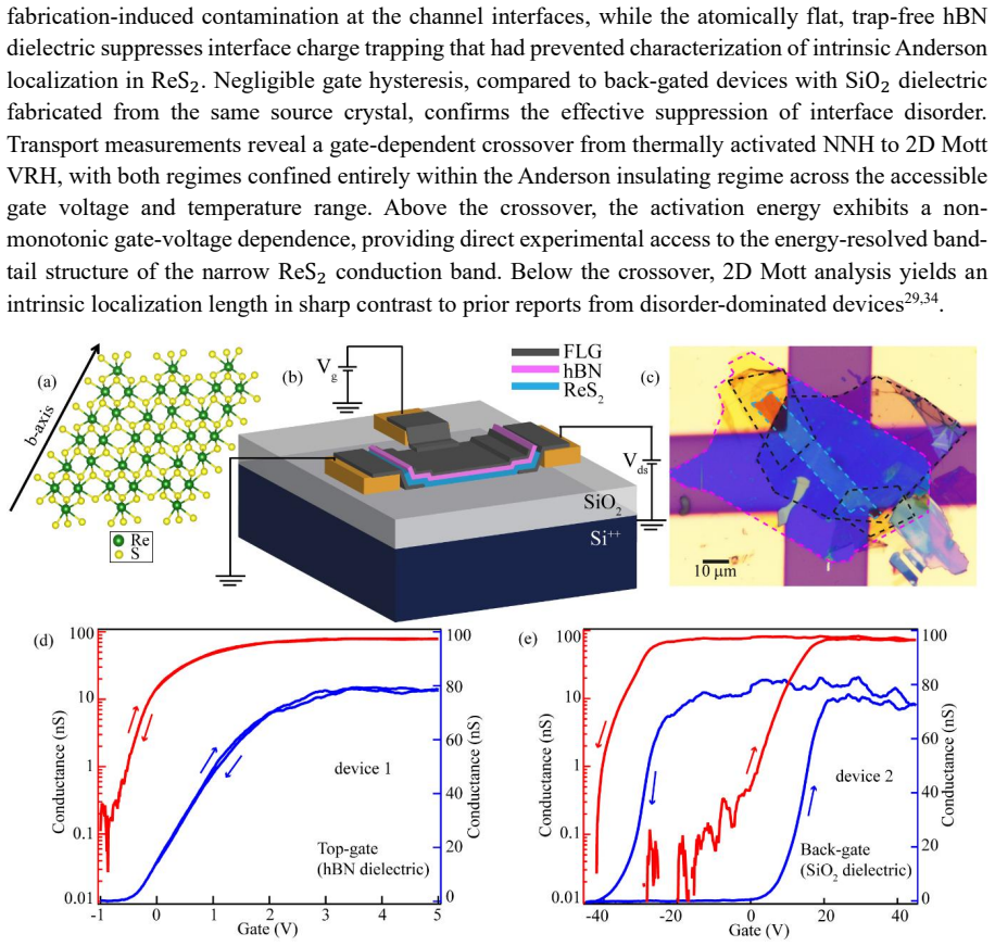
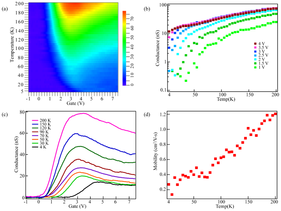
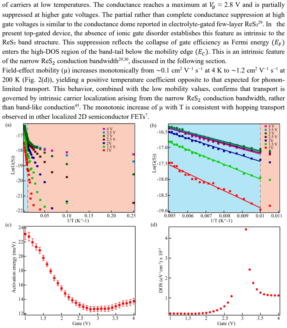
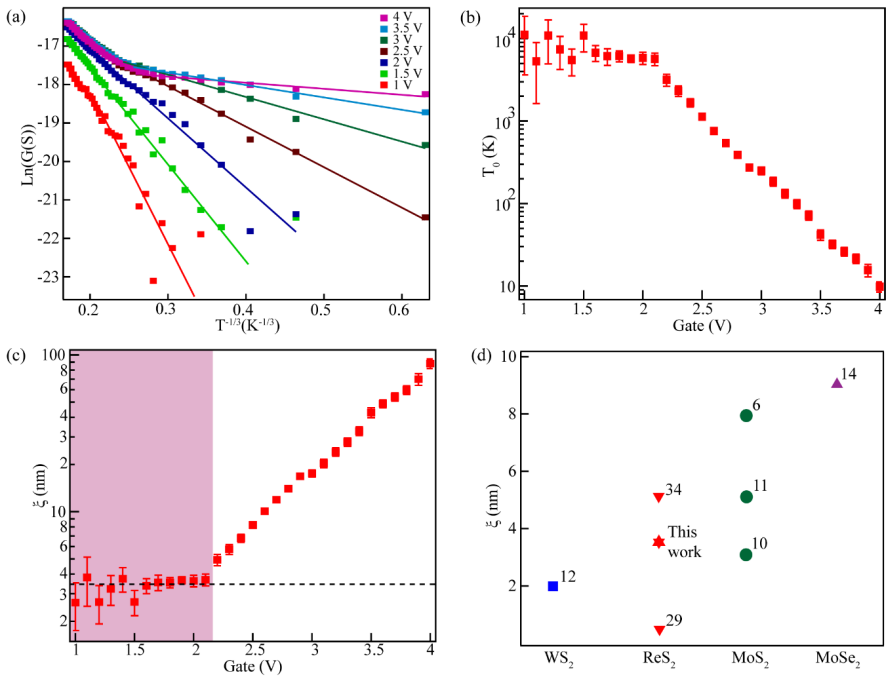
By eliminating extrinsic fabrication-induced disorder through all-dry van der Waals assembly and suppressing interface charge trapping through a hexagonal boron nitride gate dielectric, intrinsic Anderson localization is observed in few-layer ReS2. Temperature-dependent transport reveals a crossover from nearest-neighbor hopping to two-dimensional Mott variable-range hopping. The non-monotonic gate-voltage dependence of activation energy provides direct access to the energy-resolved band-tail density of states of the ReS2 conduction band. 2D Mott VRH analysis yields a localization length of (3.5 ± 0.1) nm, an order of magnitude larger than in disorder-dominated devices.
What carries the argument
2D Mott variable-range hopping arising in the ReS2 conduction band once extrinsic disorder is removed by all-dry assembly and hBN dielectric.
If this is right
- Crossover from nearest-neighbor to 2D Mott VRH occurs as temperature is lowered.
- Activation energy shows non-monotonic dependence on gate voltage that directly maps band-tail density of states.
- Localization length reaches (3.5 ± 0.1) nm, an order of magnitude larger than in disorder-dominated samples.
- Quantitative characterization of intrinsic Anderson localization becomes possible in ReS2.
Where Pith is reading between the lines
- Clean assembly techniques may isolate intrinsic localization in other narrow-bandwidth 2D materials.
- Reducing extrinsic disorder could improve low-temperature conductivity in ReS2 devices by increasing the effective localization length.
- Anderson localization may impose a fundamental low-temperature limit on transport even in the absence of fabrication defects.
Load-bearing premise
The temperature dependence and gate-voltage behavior arise purely from intrinsic Anderson localization in the ReS2 conduction band rather than any residual extrinsic disorder or interface effects.
What would settle it
If similarly fabricated devices instead exhibit temperature dependence or localization lengths matching strong extrinsic disorder, such as much smaller values or inconsistent hopping exponents, the intrinsic claim would be falsified.
Figures
read the original abstract
Electron localization phenomena are expected to play an important role in the transport properties of two-dimensional materials. Rhenium disulfide (ReS$_2$), with its narrow conduction bandwidth, is uniquely susceptible to this effect. However, extrinsic disorder caused by fabrication methods obscures inherent localization behavior arising from reduced dimensionality and degrades transport properties. We report intrinsic Anderson localization in few-layer ReS$_2$ by eliminating extrinsic fabrication-induced disorder through all-dry van der Waals assembly and suppressing interface charge trapping through a hexagonal boron nitride (hBN) gate dielectric. Temperature-dependent transport reveals a crossover from nearest-neighbor hopping to two-dimensional (2D) Mott variable-range hopping (VRH). The non-monotonic gate-voltage dependence of activation energy provides direct access to the energy-resolved band-tail density of states of the ReS$_2$ conduction band. 2D Mott VRH yields a localization length of (3.5 $\pm$ 0.1) nm, an order of magnitude larger than disorder-dominated devices, providing a quantitative characterization of intrinsic Anderson localization in ReS$_2$.
Editorial analysis
A structured set of objections, weighed in public.
Referee Report
Summary. The manuscript reports observation of intrinsic Anderson localization in few-layer ReS₂ achieved via all-dry van der Waals assembly and hBN gate dielectric to suppress extrinsic disorder. Temperature-dependent transport data show a crossover from nearest-neighbor hopping to 2D Mott variable-range hopping (VRH), while the non-monotonic gate-voltage dependence of activation energy is interpreted as direct access to the energy-resolved band-tail density of states in the ReS₂ conduction band. From the 2D Mott VRH fit the authors extract a localization length of (3.5 ± 0.1) nm, stated to be an order of magnitude larger than in disorder-dominated devices.
Significance. If the attribution to purely intrinsic Anderson localization is robust, the work supplies a quantitative benchmark for the localization length in clean few-layer ReS₂ and illustrates how fabrication-induced disorder can mask the intrinsic effects arising from the material’s narrow bandwidth and reduced dimensionality.
major comments (2)
- [temperature-dependent transport section] temperature-dependent transport section: the central extraction of the localization length from the 2D Mott VRH fit is load-bearing for the quantitative claim, yet the manuscript provides no explicit information on the temperature window used for the fit, the goodness-of-fit metric, or systematic comparison against alternative models (e.g., 3D VRH or Efros-Shklovskii VRH) that could produce comparable temperature dependence.
- [gate-voltage dependence sections] gate-voltage dependence sections: the interpretation that the non-monotonic activation-energy behavior directly maps the band-tail DOS assumes that residual interface traps and extrinsic disorder have been fully eliminated; without quantitative control experiments (e.g., comparison devices with different dielectrics or explicit trap-density estimates) this attribution remains the weakest link in the central claim.
minor comments (2)
- The statement that the localization length is “an order of magnitude larger” should be supported by explicit numerical comparison to the cited disorder-dominated devices rather than left as a qualitative claim.
- Figure captions and methods should specify the exact functional form of the VRH expression employed (including any prefactors) and the procedure used to obtain the quoted uncertainty of ±0.1 nm.
Simulated Author's Rebuttal
We thank the referee for the constructive feedback on our manuscript. We address the two major comments point by point below. Where the concerns identify missing details or insufficient justification, we will revise the manuscript accordingly.
read point-by-point responses
-
Referee: [temperature-dependent transport section] temperature-dependent transport section: the central extraction of the localization length from the 2D Mott VRH fit is load-bearing for the quantitative claim, yet the manuscript provides no explicit information on the temperature window used for the fit, the goodness-of-fit metric, or systematic comparison against alternative models (e.g., 3D VRH or Efros-Shklovskii VRH) that could produce comparable temperature dependence.
Authors: We agree that these details are essential for the robustness of the localization-length extraction. In the revised manuscript we will explicitly state the temperature window (approximately 20–80 K) over which the 2D Mott VRH fit was performed, report the goodness-of-fit metric (R² > 0.99 for the linear regime in the appropriate plot), and add a supplementary analysis comparing the data to 3D Mott VRH and Efros-Shklovskii VRH. The comparison will show that only the 2D Mott form yields a consistent localization length across the measured gate voltages while the alternative models produce unphysical parameters or poorer fits outside narrow temperature intervals. revision: yes
-
Referee: [gate-voltage dependence sections] gate-voltage dependence sections: the interpretation that the non-monotonic activation-energy behavior directly maps the band-tail DOS assumes that residual interface traps and extrinsic disorder have been fully eliminated; without quantitative control experiments (e.g., comparison devices with different dielectrics or explicit trap-density estimates) this attribution remains the weakest link in the central claim.
Authors: The all-dry van der Waals assembly combined with hBN gating is chosen precisely because prior literature has established that these techniques suppress extrinsic disorder and interface traps to levels below the intrinsic band-tail effects in narrow-bandwidth 2D materials. The observed non-monotonic activation energy versus gate voltage is a signature not reproduced in conventional SiO₂-supported devices and is consistent with the expected energy dependence of the ReS₂ conduction-band tail. Nevertheless, we acknowledge that the manuscript would benefit from a more quantitative discussion. In revision we will expand the relevant section to include (i) a comparison of extracted mobilities and localization lengths with literature values for hBN-encapsulated versus SiO₂-supported ReS₂, and (ii) an estimate of residual trap density drawn from published capacitance-voltage data on similar hBN/ReS₂ stacks. We do not have new control-device data in the present study, but the added discussion will make the assumptions explicit and cite supporting evidence from the fabrication method. revision: partial
Circularity Check
No significant circularity; experimental observation self-contained
full rationale
The paper is an experimental report of Anderson localization in ReS2 via all-dry assembly and hBN gating. Central results (crossover to 2D Mott VRH, non-monotonic activation energy, localization length 3.5 nm from standard fitting) are extracted from transport data using established models, with no derivation chain, self-definitional equations, fitted inputs renamed as predictions, or load-bearing self-citations. The work stands on external benchmarks (temperature dependence, gate-voltage sweeps) without reducing to its own inputs by construction.
Axiom & Free-Parameter Ledger
Reference graph
Works this paper leans on
-
[1]
Castellanos-Gomez, M
A. Castellanos-Gomez, M. Buscema, R. Molenaar, V. Singh, L. Janssen, H. S. J. Van Der Zant, and G. A. Steele, Deterministic transfer of two-dimensional materials by all-dry viscoelastic stamping, 2D Mater. 1, 011002 (2014)
2014
-
[2]
Zhou et al., Stacking‐Order‐Driven Optical Properties and Carrier Dynamics in ReS 2, Advanced Materials 32, 1908311 (2020)
Y. Zhou et al., Stacking‐Order‐Driven Optical Properties and Carrier Dynamics in ReS 2, Advanced Materials 32, 1908311 (2020)
2020
-
[3]
Van Der Laan et al., Stacking-Order-Dependent Excitonic Properties Reveal Interlayer Interactions in Bulk ReS2, ACS Photonics 10, 3115 (2023)
M. Van Der Laan et al., Stacking-Order-Dependent Excitonic Properties Reveal Interlayer Interactions in Bulk ReS2, ACS Photonics 10, 3115 (2023)
2023
-
[4]
Poudyal, P
S. Poudyal, P. K. Barman, R. Biswas, K. Kravtsov, B. Biswal, R. Yadav, V. Raghunathan, I. Kruglov, D. A. Ghazaryan, and A. Misra, Stacking and Layer Parity Dependent Photoluminescence in ReS 2, Advanced Optical Materials 2403265 (2025)
2025
-
[5]
Dhara, D
A. Dhara, D. Chakrabarty, P. Das, A. K. Pattanayak, S. Paul, S. Mukherjee, and S. Dhara, Additional excitonic features and momentum-dark states in ReS 2, Phys. Rev. B 102, 161404 (2020)
2020
-
[6]
Tongay et al., Monolayer behaviour in bulk ReS2 due to electronic and vibrational decoupling, Nat Commun 5, 3252 (2014)
S. Tongay et al., Monolayer behaviour in bulk ReS2 due to electronic and vibrational decoupling, Nat Commun 5, 3252 (2014)
2014
-
[7]
K. K. Kim, A. Hsu, X. Jia, S. M. Kim, Y. Shi, M. Dresselhaus, T. Palacios, and J. Kong, Synthesis and Characterization of Hexagonal Boron Nitride Film as a Dielectric Layer for Graphene Devices, ACS Nano 6, 8583 (2012)
2012
-
[8]
C. R. Dean et al., Boron nitride substrates for high-quality graphene electronics, Nature Nanotech 5, 722 (2010)
2010
-
[9]
N. F. Mott, N. F. Mott, and E. A. Davis, Electronic Processes in Non-Crystalline Materials, 2. ed (Clarendon Press, Oxford, 1979)
1979
-
[10]
A. L. Efros and B. I. Shklovskii, Coulomb gap and low temperature conductivity of disordered systems, J. Phys. C: Solid State Phys. 8, L49 (1975)
1975
-
[11]
Qiu et al., Hopping transport through defect-induced localized states in molybdenum disulphide, Nat Commun 4, 2642 (2013)
H. Qiu et al., Hopping transport through defect-induced localized states in molybdenum disulphide, Nat Commun 4, 2642 (2013)
2013
-
[12]
N. Ali, M. Lee, F. Ali, T. D. Ngo, H. Park, H. Shin, and W. J. Yoo, Percolation -Based Metal–Insulator Transition in Black Phosphorus Field Effect Transistors, ACS Appl. Mater. Interfaces 15, 13299 (2023)
2023
-
[13]
Ghatak, A
S. Ghatak, A. N. Pal, and A. Ghosh, Nature of Electronic States in Atomically Thin MoS 2 Field-Effect Transistors, ACS Nano 5, 7707 (2011)
2011
-
[14]
J. Xue, S. Huang, J.-Y. Wang, and H. Q. Xu, Mott variable-range hopping transport in a MoS2 nanoflake, RSC Adv. 9, 17885 (2019)
2019
-
[15]
Singha, A
A. Singha, A. P, A. Paul, S. K. Shetty, K. Watanabe, T. Taniguchi, A. Ghosh, and S. Mitra, Correlating Carrier Localization to Optoelectronic Behavior of Monolayer MoS 2, ACS Appl. Mater. Interfaces acsami.5c08111 (2025)
2025
-
[16]
Ovchinnikov, A
D. Ovchinnikov, A. Allain, Y.-S. Huang, D. Dumcenco, and A. Kis, Electrical Transport Properties of Single-Layer WS 2, ACS Nano 8, 8174 (2014)
2014
-
[17]
Chen et al., Highly Oriented Atomically Thin Ambipolar MoSe 2 Grown by Molecular Beam Epitaxy, ACS Nano 11, 6355 (2017)
M.-W. Chen et al., Highly Oriented Atomically Thin Ambipolar MoSe 2 Grown by Molecular Beam Epitaxy, ACS Nano 11, 6355 (2017)
2017
-
[18]
N. Ali, M. Lee, F. Ali, H. Shin, T. D. Ngo, K. Watanabe, T. Taniguchi, B. Oh, and W. J. Yoo, Gate - Controlled Metal to Insulator Transition in Black Phosphorus Nanosheet-Based Field Effect Transistors, ACS Appl. Nano Mater. 5, 18376 (2022)
2022
-
[19]
Ovchinnikov, F
D. Ovchinnikov, F. Gargiulo, A. Allain, D. J. Pasquier, D. Dumcenco, C. -H. Ho, O. V. Yazyev, and A. Kis, Disorder engineering and conductivity dome in ReS2 with electrolyte gating, Nat Commun 7, 12391 (2016)
2016
-
[20]
Zhang, Y
E. Zhang, Y. Jin, X. Yuan, W. Wang, C. Zhang, L. Tang, S. Liu, P. Zhou, W. Hu, and F. Xiu, ReS 2 ‐ Based Field‐Effect Transistors and Photodetectors, Adv Funct Materials 25, 4076 (2015)
2015
discussion (0)
Sign in with ORCID, Apple, or X to comment. Anyone can read and Pith papers without signing in.