REVIEW 2 major objections 6 minor 40 references
High yield, low disorder Si/SiGe heterostructures for spin qubit devices manufactured in a BiCMOS pilot line
T0 review · 2 major / 6 minor · reviewed 2026-08-15 · deepseek-v4-flash
Pith's one-line read This paper claims that a 200 mm BiCMOS pilot line reproducibly yields low-disorder Si/SiGe heterostructures, with peak mobility $(4.25\pm0.17)\times10^5$ cm$^2$/Vs and percolation density $(5.9\pm0.18)\times10^{10}$ cm$^{-2}$ across six…
desk verdict Useful BiCMOS Si/SiGe process benchmark with clean transport data, but the multi-wafer statistics rest on one center device per wafer and the 'high yield' title outruns the data. read the letter →
The pith
A machine-rendered reading of the paper's core claim, the machinery that carries it, and where it could break.
The reading
What carries the argument
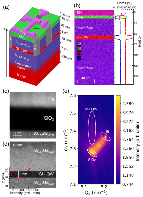
The load-bearing measurement platform is the Hall-bar field-effect transistor (HB-FET): an optically patterned Hall bar with a TiN top gate and a plasma-deposited SiO$_2$ dielectric whose stack mirrors a qubit gate stack while giving direct magnetotransport access to the two-dimensional electron gas in the 8 nm Si quantum well. Three quantitative probes carry the argument: the carrier density versus gate voltage slope yields the stack capacitance and therefore dielectric and barrier thickness; the density-dependent Hall mobility ($\sigma_{xx} = ne\mu$) separates scattering regimes through the power-law exponent $\alpha$; and a fit of low-density conductivity to the percolation law $\sigma_{xx} \propto (n - n_p)^p$ with $p = 1.31$ extracts the percolation density $n_p$, a direct low-density disorder metric. These probes convert wafer-scale uniformity and run-to-run reproducibility into numbers.
What would settle it
Measure transport on a dense map of devices across whole wafers from several runs, including edge dies and multiple radii. If a significant fraction of devices shows peak mobility below the reported distribution or percolation density above roughly $1\times10^{11}$ cm$^{-2}$, the claimed wafer-scale homogeneity and run-to-run reproducibility would be refuted.
Extended reading notes
Core claim
The central discovery is that an industry-standard 200 mm BiCMOS pilot line produces shallow undoped Si/SiGe quantum wells whose transport properties are both high and tightly distributed. Across wafers A to F the maximum Hall mobility averages $(4.25\pm0.17)\times10^5$ cm$^2$/Vs, and across one wafer it averages $(4.20\pm0.28)\times10^5$ cm$^2$/Vs; the percolation densities are $(5.9\pm0.18)\times10^{10}$ cm$^{-2}$ and $(6.24\pm0.33)\times10^{10}$ cm$^{-2}$, respectively. The authors interpret the low-density mobility rise ($\alpha\approx2.47$) as remote-impurity Coulomb scattering and the low percolation threshold as evidence of a low-disorder landscape in the quantum well, comparable to or better than state-of-the-art field-effect stacks used for quantum devices. Structural imaging supports the electrical picture: no residual Si cap, no significant Ge pile-up at the gate interface, abrupt quantum-well interfaces, and the expected $1.29\%$ tensile strain in the Si channel.
Load-bearing premise
The claim of reproducibility and uniformity rests on assuming that one device from the center of each of six wafers, plus twelve devices from one wafer, represent the full wafers; if defective or nonuniform regions fell outside those probed spots, the narrow reported distributions would overstate process stability.
Editorial extensions
If this is right
- Across multiple fabrication runs a single 200 mm line can deliver peak 2DEG mobility above $4\times10^5$ cm$^2$/Vs, matching the best field-effect stacks reported for quantum devices.
- Percolation densities near $6\times10^{10}$ cm$^{-2}$ mean the quantum well stays low-disorder at the low carrier densities where gate-defined quantum dots are operated.
- The few-percent spread in capacitance, mobility, and percolation density across a wafer means many nominally identical qubit devices can be made side by side, a prerequisite for high-yield processor fabrication.
- Because the growth chemistry is standard silane and germane reduced-pressure CVD, the same process can be applied to isotopically purified $^{28}$Si to obtain nuclear-spin-free heterostructures for long-coherence qubits.
- The gate-stack characterization shows the sacrificial Si cap is fully consumed without leaving Ge pile-up, removing a known source of disorder at the dielectric interface.
Reading between the lines
- Editorial inference: the single edge-device outlier with suppressed peak mobility hints that practical yield could be increased by excluding the wafer edge, but the sparse sampling cannot establish an edge-exclusion rule.
- Editorial inference: transport metrics are proxies; the decisive follow-up is to build quantum dots on these wafers and measure charge noise, valley splitting, and single-electron operation directly.
- Editorial inference: the observed saturation of carrier density at high gate voltage, attributed to electrons tunneling into dielectric-interface traps, may cap the usable density range for devices; whether this limits qubit operation is not addressed here.
- Editorial inference: a direct next experiment is growing the same stack with an isotopically enriched $^{28}$Si quantum well and checking that mobility and percolation density survive the isotope switch, as the authors expect from the growth chemistry.
Signed reviews
Editorial analysis
A structured set of objections, weighed in public.
Referee Report
Summary. This manuscript reports magnetotransport characterization of Hall-bar field-effect transistors fabricated on Si/SiGe heterostructures grown in a 200 mm BiCMOS pilot line. The authors measure carrier density, Hall mobility, and percolation density at 1.5 K for one center device from each of six nominally identical wafers and for 12 additional devices across one wafer (wafer A). They report an average peak mobility of (4.25±0.17)×10^5 cm^2/Vs and a percolation density of (5.9±0.18)×10^10 cm^-2 across the six wafers, with similar wafer-scale values, and conclude that the process yields low-disorder, homogeneous heterostructures suitable for scalable spin-qubit devices. Structural characterization (STEM/EDX, XRD) is used to support layer thickness, interface sharpness, and strain claims.
Significance. If the reported uniformity and reproducibility hold, the paper demonstrates that an industry-standard BiCMOS pilot line can produce Si/SiGe field-effect stacks with transport properties comparable to or better than current state-of-the-art qubit-compatible stacks, which is an important step for scalable spin qubit manufacturing. Strengths of the work include the use of standard transport formulas with an externally sourced percolation exponent (p = 1.31), cross-laboratory validation of two devices, and quantitative structural analysis (interface widths from STEM, strain from XRD). The main caveat is that the central reproducibility claim rests on a small, center-selected sample, with an acknowledged edge outlier on wafer A that is not sampled on the other wafers.
major comments (2)
- [Magnetotransport characterization and Fig. 2] The wafer-to-wafer reproducibility claim is built on one center-selected device per wafer (wafers A–F, six devices total), while the wafer-scale study of wafer A includes a near-edge device whose peak mobility and high-density exponent (alpha = -0.6) lie far outside the reported standard deviations. Because no edge or near-edge devices were measured on wafers B–F, the quoted wafer-to-wafer averages (mu = (4.25±0.17)×10^5 cm^2/Vs, n_p = (5.9±0.18)×10^10 cm^-2) may systematically exclude the kind of degradation that the edge outlier reveals. The conclusion of 'homogeneous' wafer-scale performance is therefore stronger than the data support; the authors should either present edge-location measurements from multiple wafers or explicitly restrict the uniformity claim to the central wafer area.
- [Title, abstract, and conclusion] The title and concluding section claim 'high yield,' but the manuscript contains no yield statistics: no definition of a working device, no pass/fail criterion, and no fraction of devices meeting a performance specification. The reported averages are computed from a small, selected set of devices (one center device per wafer for six wafers, plus 12 devices on one wafer). To support the 'high yield' claim, the authors need to provide yield data or at least a clear statement of the selection procedure; otherwise the claim should be removed or qualified.
minor comments (6)
- [Fig. 2c paragraph] The text contains a duplicated word: 'If if we consider local-field corrections' should read 'If we consider local-field corrections.'
- [Fig. 1 caption] The abbreviation 'HADDF' in the Fig. 1 caption should be 'HAADF' to match the high-angle annular dark-field terminology used in the main text.
- [Quantum well interface width, Fig. 1d] The top interface width is reported as 4*tau_top = 0.79 nm while the bottom is reported as tau_bot = 1.04 nm; please clarify whether the 4*tau parameter was applied consistently and state the definition for each interface.
- [Transport extraction methods] Please specify the magnetic-field range and the B->0 extrapolation procedure used to extract mobility from rho_xx and rho_xy, and define n_min in the percolation fitting range (n_min <= n_range <= 1.2×10^11 cm^-2).
- [Figure 2b and capacitance statistics] The caption states that the red dashed line is a linear fit to the mean trend; please clarify whether the reported capacitance statistics come from fits to individual devices or from fits to the mean curve.
- [Affiliation and references] There are minor typographical issues: 'F orschungszentrum' should be 'Forschungszentrum', the license should be identified accurately as CC BY-NC-SA 4.0, and reference groupings such as '192' and '23171926' should be formatted as separate citations.
Circularity Check
No circularity: transport parameters are extracted with standard formulas and external percolation exponents, with self-citations used only as baseline and process references.
full rationale
The derivation chain is self-contained. Carrier density n is obtained from the standard Hall relation ρxy = B⊥/(e n) and mobility from σxx = n e μ (section on magnetotransport characterization and Fig. 2c), with no target transport quantity used as an input. The percolation density is extracted by fitting σxx ∝ (n − np)^p with p = 1.31 taken from Tracy et al. [35], an external literature value, so the fit parameter np is not preset by the paper's own claims. Capacitance is checked against a geometric estimate from STEM thicknesses with standard dielectric constants, agreeing to within 1%, which is an independent consistency check rather than a circular reuse of the result. Comparisons of mobility and percolation density are made against external benchmarks (e.g., refs. 17, 19, 26). Self-citations appear only as process-description references ([20], [18]) and as a baseline for improvement ('substantial improvement to our previous work [20]'); none of these citations is used to forbid alternatives or to define the target quantities. The reader-identified sampling limitation—one center device per wafer for wafers B–F and one edge outlier in wafer A—is a statistical representativeness concern, not a circularity: it affects how broadly the wafer-to-wafer uniformity claim generalizes but does not make any extracted value depend on the conclusion. No fitted parameter is renamed as a prediction, and no result is assumed in its own derivation. The title's 'high yield' wording is unsupported by yield statistics, but that is a correctness or evidence concern, not circularity.
Assumptions & free parameters
free parameters (3)
- Low-density power-law exponent alpha =
2.47 (median)
- High-density power-law exponent alpha =
-0.12 (median)
- STEM interface-width sigmoid parameters =
4 tau_top = 0.79 nm, tau_bot = 1.04 nm
assumptions (5)
- standard math 2DEG transport formulas rho_xy = B/(e n) and sigma_xx = n e mu
- domain assumption Percolation conductivity model sigma_xx proportional to (n - np)^p with p = 1.31
- domain assumption Parallel-plate capacitor model for gate-induced density
- domain assumption Hall bar 2DEG transport is a proxy for disorder relevant to spin qubit devices
- domain assumption Single 2DEG channel with negligible parallel conduction
Cite this review
Pith. "Pith review of High yield, low disorder Si/SiGe heterostructures for spin qubit devices manufactured in a BiCMOS pilot line." pith.science (2026). https://pith.science/paper/KX6XLMLE
@misc{pith2026250614660,
  author       = {Pith},
  title        = {Pith review of: High yield, low disorder Si/SiGe heterostructures for spin qubit devices manufactured in a BiCMOS pilot line},
  year         = {2026},
  howpublished = {\url{https://pith.science/paper/KX6XLMLE}},
  note         = {Machine review of arXiv:2506.14660}
}
abstract
The prospect of achieving fault-tolerant quantum computing with semiconductor spin qubits in Si/SiGe heterostructures relies on the integration of a large number of identical devices, a feat achievable through a scalable (Bi)CMOS manufacturing approach. To this end, both the gate stack and the Si/SiGe heterostructure must be of high quality, exhibiting uniformity across the wafer and consistent performance across multiple fabrication runs. Here, we report a comprehensive investigation of Si/SiGe heterostructures and gate stacks, fabricated in an industry-standard 200 mm BiCMOS pilot line. We evaluate the homogeneity and reproducibility by probing the properties of the two-dimensional electron gas (2DEG) in the shallow silicon quantum well through magnetotransport characterization of Hall bar-shaped field-effect transistors at 1.5 K. Across all the probed wafers, we observe minimal variation of the 2DEG properties, with an average maximum mobility of $(4.25\pm0.17)\times 10^{5}$ cm$^{2}$/Vs and low percolation carrier density of $(5.9\pm0.18)\times 10^{10}$ cm$^{-2}$ evidencing low disorder potential in the quantum well. The observed narrow statistical distribution of the transport properties highlights the reproducibility and the stability of the fabrication process. Furthermore, wafer-scale characterization of a selected individual wafer evidenced the homogeneity of the device performances across the wafer area. Based on these findings, we conclude that our material and processes provide a suitable platform for the development of scalable, Si/SiGe-based quantum devices.
Figures

Reference graph
Works this paper leans on
-
[1]
merlin.mbs aapmrev4-1.bst 2010-07-25 4.21a (PWD, AO, DPC) hacked
FUNCTION id.bst "merlin.mbs aapmrev4-1.bst 2010-07-25 4.21a (PWD, AO, DPC) hacked" ENTRY address archive archivePrefix author bookaddress booktitle chapter collaboration doi edition editor eid eprint howpublished institution isbn issn journal key language month note number organization pages primaryClass publisher school SLACcitation series title translat...
2010
-
[2]
merlin.mbs aipauth4-1.bst 2010-07-25 4.21a (PWD, AO, DPC) hacked
FUNCTION id.bst "merlin.mbs aipauth4-1.bst 2010-07-25 4.21a (PWD, AO, DPC) hacked" ENTRY address archive archivePrefix author bookaddress booktitle chapter collaboration doi edition editor eid eprint howpublished institution isbn issn journal key language month note number organization pages primaryClass publisher school SLACcitation series title translat...
2010
-
[3]
merlin.mbs aipnum4-1.bst 2010-07-25 4.21a (PWD, AO, DPC) hacked
FUNCTION id.bst "merlin.mbs aipnum4-1.bst 2010-07-25 4.21a (PWD, AO, DPC) hacked" ENTRY address archive archivePrefix author bookaddress booktitle chapter collaboration doi edition editor eid eprint howpublished institution isbn issn journal key language month note number organization pages primaryClass publisher school SLACcitation series title translati...
2010
-
[4]
merlin.mbs apsrev4-1.bst 2010-07-25 4.21a (PWD, AO, DPC) hacked
FUNCTION id.bst "merlin.mbs apsrev4-1.bst 2010-07-25 4.21a (PWD, AO, DPC) hacked" ENTRY address archive archivePrefix author bookaddress booktitle chapter collaboration doi edition editor eid eprint howpublished institution isbn issn journal key language month note number organization pages primaryClass publisher school SLACcitation series title translati...
2010
-
[5]
merlin.mbs apsrmp4-1.bst 2010-07-25 4.21a (PWD, AO, DPC) hacked
FUNCTION id.bst "merlin.mbs apsrmp4-1.bst 2010-07-25 4.21a (PWD, AO, DPC) hacked" ENTRY address archive archivePrefix author bookaddress booktitle chapter collaboration doi edition editor eid eprint howpublished institution isbn issn journal key language month note number organization pages primaryClass publisher school SLACcitation series title translati...
2010
-
[6]
author author G. Hu , author W. W. \ Huang , author R. Cai , author L. Wang , author C. H. \ Yang , author G. Cao , author X. Xue , author P. Huang , \ and\ author Y. He ,\ title title Single-electron spin qubits in silicon for quantum computing , \ @noop journal journal Intelligent Computing \ volume 4 ,\ pages 0115 ( year 2025 ) NoStop
work page 2025
-
[7]
author author S. Neyensa , author O. K. \ Zietz , author T. F. \ Watson , author F. Luthi , author A. Nethwewala , author H. C. \ George , author E. Henry , author M. Islam , author A. J. \ Wagner , author F. Borjans , author E. J. \ Connors , author J. Corrigan , author D. K. \ Matthew J. Curry , author R. Kotlyar , author L. F. \ Lampert , author M. T. ...
work page 2024
-
[8]
author author H. C. \ George , author M. T. \ Mądzik , author E. M. \ Henry , author A. J. \ Wagner , author M. M. \ Islam , author F. Borjans , author E. J. \ Connors , author J. Corrigan , author M. Curry , author M. K. \ Harper , author D. Keith , author L. Lampert , author F. Luthi , author F. A. \ Mohiyaddin , author S. Murcia , author R. Nair , auth...
work page 2025
Show all 40 references
-
[9]
author author F. K. \ Unseld , author M. Meyer , author M. T. \ Mądzik , author F. Borsoi , author S. L. \ de Snoo , author S. V. \ Amitonov , author A. Sammak , author G. Scappucci , author M. Veldhorst , \ and\ author L. M. K. \ Vandersypen ,\ title title A 2 D quantum dot a...
2023
-
[10]
Harvey ,\ title title Quantum dots / spin qubits , \ @noop journal journal Oxford Research Encyclopedia of Physics \ ( year 2022 ) NoStop
author author S. Harvey ,\ title title Quantum dots / spin qubits , \ @noop journal journal Oxford Research Encyclopedia of Physics \ ( year 2022 ) NoStop
2022
-
[11]
Wang , author S.-M
author author N. Wang , author S.-M. \ Wang , author R.-Z. \ Zhang , author J.-M. \ Kang , author W.-L. \ Lu , author H.-O. \ Li , author G. Cao , author B.-C. \ Wang , \ and\ author G.-P. \ Guo ,\ title title Pursuing high-fidelity control of spin qubits in natural Si / SiGe ...
2024
-
[12]
author author A. R. \ Mills , author C. R. \ Guinn , author M. J. \ Gullans , author A. J. \ Sigillito , author M. M. \ Feldman , author E. Nielsen , \ and\ author J. R. \ Petta ,\ title title Two-qubit silicon quantum processor with operation fidelity exceeding 99\
-
[13]
Kobayashi , author J
author author T. Kobayashi , author J. Salfi , author C. Chua , author J. van der Heijden , author M. G. \ House , author D. Culcer , author W. D. \ Hutchison , author B. C. \ Johnson , author J. C. \ McCallum , author H. Riemann , author N. V. \ Abrosimov , author P. Becker ,...
2021
-
[14]
Struck , author A
author author T. Struck , author A. Hollmann , author F. Schauer , author O. Fedorets , author A. Schmidbauer , author K. Sawano , author H. Riemann , author N. V. \ Abrosimov , author Łukasz Cywiński , author D. Bougeard , \ and\ author L. R. \ Schreiber ,\ title title Low-fr...
2020
-
[15]
author author S. G. J. \ Philips , author M. T. \ Mądzik , author S. V. \ Amitonov , author S. L. \ de Snoo , author M. Russ , author N. Kalhor , author C. Volk , author W. I. L. \ Lawrie , author D. Brousse , author L. Tryputen , author B. Paquelet Wuetz , author A. Sammak , ...
2022
-
[16]
author author Huckemann , author Till , author Muster , author Pascal , author Langheinrich , author Wolfram , author Brackmann , author Varvara , author Friedrich , author Michael , author Komerički , author N. D. , author Diebel , author L. K. , author Stieß , author Verena ...
2025
-
[17]
author author L. M. K. \ Vandersypen , author H. Bluhm , author J. S. \ Clarke , author A. S. \ Dzurak , author R. Ishihara , author A. Morello , author D. J. \ Reilly , author L. R. \ Schreiber , \ and\ author M. Veldhorst ,\ title title Interfacing spin qubits in quantum dot...
2017
-
[18]
Künne , author A
author author M. Künne , author A. Willmes , author M. Oberländer , author C. Gorjaew , author J. D. \ Teske , author H. Bhardwaj , author M. Beer , author E. Kammerloher , author R. Otten , author I. Seidler , author R. Xue , author L. R. \ Schreiber , \ and\ author H. Bluhm ...
2024
-
[19]
Xue , author M
author author R. Xue , author M. Beer , author I. Seidler , author S. Humpohl , author J.-S. \ Tu , author S. Trellenkamp , author T. Struck , author H. Bluhm , \ and\ author L. R. \ Schreiber ,\ title title Si/SiGe QuBus for single electron information-processing devices with...
2024
-
[20]
Li , author L
author author R. Li , author L. Petit , author D. P. \ Franke , author J. P. \ Dehollain , author J. Helsen , author M. Steudtner , author N. K. \ Thomas , author Z. R. \ Yoscovits , author K. J. \ Singh , author S. Wehner , author L. M. K. \ Vandersypen , author J. S. \ Clark...
2018
-
[21]
Scappucci , author P
author author G. Scappucci , author P. J. \ Taylor , author J. R. \ Williams , author T. Ginley , \ and\ author S. Law ,\ title title Crystalline materials for quantum computing: Semiconductor heterostructures and topological insulators exemplars , \ @noop journal journal MRS ...
2021
-
[22]
author author D. D. \ Esposti , author L. E. A. \ Stehouwer , author Önder Gül , author N. Samkharadze , author C. Déprez , author M. Meyer , author I. N. \ Meijer , author L. Tryputen , author S. Karwal , author M. Botifoll , author J. Arbiol , author S. V. \ Amitonov , autho...
2024
-
[23]
author author L. K. \ Diebel , author L. G. \ Zinkl , author A. Hötzinger , author F. Reichmann , author M. Lisker , author Y. Yamamoto , \ and\ author D. Bougeard ,\ title title Impact of biased cooling on the operation of undoped silicon quantum well field-effect devices , \...
2025
-
[24]
Paquelet Wuetz , author P
author author B. Paquelet Wuetz , author P. L. \ Bavdaz , author L. A. \ Yeoh , author R. Schouten , author H. van der Does , author M. Tiggelman , author D. Sabbagh , author A. Sammak , author C. G. \ Almudever , author F. Sebastiano , author J. S. \ Clarke , author M. Veldho...
2020
-
[25]
Reichmann , author A
author author F. Reichmann , author A. Mistroni , author Y. Yamamoto , author P. Kulse , author S. Marschmeyer , author D. Wolansky , author O. Fursenko , author M. H. \ Zöllner , author G. Capellini , author L. Diebel , author D. Bougeard , \ and\ author M. Lisker ,\ title ti...
2024
-
[26]
Wild , author J
author author A. Wild , author J. Kierig , author J. Sailer , author J. W. \ Ager , author E. E. \ Haller , author G. Abstreiter , author S. Ludwig , \ and\ author D. Bougeard ,\ title title Few electron double quantum dot in an isotopically purified ^ 28 Si quantum well , \ @...
2012
-
[27]
Sailer , author V
author author J. Sailer , author V. Lang , author G. Abstreiter , author G. Tsuchiya , author K. M. \ Itoh , author J. W. A. \ III , author E. E. \ Haller , author D. Kupidura , author D. Harbusch , author S. Ludwig , \ and\ author D. Bougeard ,\ title title A Schottky top-gat...
2009
-
[28]
author author Rovaris , author Fabrizio , author Zoellner , author M. H. , author Zaumseil , author Peter , author Marzegalli , author Anna , author D. Gaspare , author Luciana , author D. Seta , author Monica , author Schroeder , author Thomas , author Storck , author Peter ,...
2019
-
[29]
author author H. K. \ Liou , author P. Mei , author U. Gennser , \ and\ author E. S. \ Yang ,\ title title Effects of Ge concentration on SiGe oxidation behavior , \ @noop journal journal Applied Physics Letters \ volume 59 ,\ pages 1200 ( year 1991 ) NoStop
1991
-
[30]
author author H. K. \ Liou , author P. Mei , author U. Gennser , \ and\ author E. S. \ Yang ,\ title title Oxidation studies of SiGe , \ @noop journal journal Journal of Applied Physics \ volume 65 ,\ pages 1724 ( year 1989 ) NoStop
1989
-
[31]
author author D. D. \ Esposti , author B. Paquelet Wuetz , author V. Fezzi , author M. Lodari , author A. Sammak , \ and\ author G. Scappucci ,\ title title Wafer-scale low-disorder 2DEG in ^ 28 Si / SiGe without an epitaxial Si cap , \ @noop journal journal Appl. Phys. Lett. ...
2022
-
[32]
Dyck , author D
author author O. Dyck , author D. N. \ Leonard , author L. F. \ Edge , author C. A. \ Jackson , author E. J. \ Pritchett , author P. W. \ Deelman , \ and\ author J. D. \ Poplawsky ,\ title title Accurate quantification of Si / SiGe interface profiles via atom probe tomography....
2017
-
[33]
Klos , author J
author author J. Klos , author J. Tröger , author J. Keutgen , author M. P. \ Losert , author N. V. \ Abrosimov , author J. Knoch , author H. Bracht , author S. N. \ Coppersmith , author M. Friesen , author O. Cojocaru-Mirédin , author L. R. \ Schreiber , \ and\ author D. Boug...
2024
-
[34]
author author T. M. \ Lu , author C.-H. \ Lee , author S.-H. \ Huang , author D. C. \ Tsui , \ and\ author C. W. \ Liu ,\ title title Upper limit of two-dimensional electron density in enhancement-mode Si / SiGe heterostructure field-effect transistors , \ @noop journal journa...
2011
-
[35]
\ Su , author Y
author author Y.-H. \ Su , author Y. Chuang , author C.-Y. \ Liu , author J.-Y. \ Li , \ and\ author T.-M. \ Lu ,\ title title Effects of surface tunneling of two-dimensional hole gases in undoped Ge / GeSi heterostructures , \ @noop journal journal Phys. Rev. Mater. \ volume ...
2017
-
[36]
Laroche , author S.-H
author author D. Laroche , author S.-H. \ Huang , author E. Nielsen , author Y. Chuang , author J.-Y. \ Li , author C. W. \ Liu , \ and\ author T. M. \ Lu ,\ title title Scattering mechanisms in shallow undoped Si / SiGe quantum wells , \ @noop journal journal AIP Advances \ v...
2015
-
[37]
Monroe , author Y
author author D. Monroe , author Y. H. \ Xie , author E. A. \ Fitzgerald , author S. P. \ J. , \ and\ author G. P. \ Watson ,\ title title Comparison of mobility‐limiting mechanisms in high‐mobility Si _ 1-x Ge _ x heterostructures , \ @noop journal journal J. Vac. Sci. Techno...
1993
-
[38]
Huang \ and\ author S
author author Y. Huang \ and\ author S. Das Sarma ,\ title title Understanding disorder in silicon quantum computing platforms: Scattering mechanisms in Si/SiGe quantum wells , \ @noop journal journal Phys. Rev. B \ volume 109 ,\ pages 125405 ( year 2024 ) NoStop
2024
-
[39]
Huang \ and\ author S
author author Y. Huang \ and\ author S. D. \ Sarma ,\ title title Bound state continuum resonance transition in a shallow quantum well , \ @noop journal journal Phys. Rev. B \ volume 110 ,\ pages 155425 ( year 2024 ) NoStop
2024
-
[40]
author author L. A. \ Tracy , author E. H. \ Hwang , author K. Eng , author G. A. \ Ten Eyck , author E. P. \ Nordberg , author K. Childs , author M. S. \ Carroll , author M. P. \ Lilly , \ and\ author S. Das Sarma ,\ title title Observation of percolation-induced two-dimensio...
2009
Reviewed August 15, 2026 · model on record in the stance chip above.
Discussion (0). Continue with ORCID to comment.