REVIEW 3 major objections 5 minor 63 references
Highly Sensitive, Fast Graphene Photodetector with Responsivity $>10^6$ A/W Using Floating Quantum Well Gate
T0 review · 3 major / 5 minor · reviewed 2026-08-14 · deepseek-v4-flash
Pith's one-line read A graphene photodetector reaches 4.4 million A/W sensitivity
desk verdict A genuinely new photogating device that could be important, but the headline responsivity depends on an uncalibrated 30 fW power, so the central number is not yet trustworthy. read the letter →
The pith
A machine-rendered reading of the paper's core claim, the machinery that carries it, and where it could break.
The reading
What carries the argument
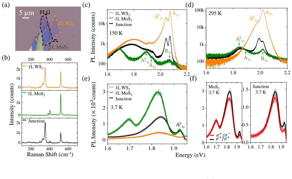
The load-bearing object is the vertical van der Waals heterojunction few-layer graphene / bilayer WS2 / monolayer MoS2, where the monolayer MoS2 acts as a floating quantum well gate for the graphene channel. The mechanism is quantum-confined photogating: ultrafast interlayer electron transfer from graphene into the MoS2 quantum well builds a stored electron population that shifts the graphene Dirac point and changes its conductance, giving high photoconductive gain. The thin WS2 layer controls both the injection rate into the well and the tunnel-back rate to graphene, and the conduction-band offset between MoS2 and graphene provides a built-in field that swiftly empties the well when light is turned off. The argument is carried by a coupled rate-equation model for the photoinduced carrier density in graphene, the electron density in the MoS2 conduction band, and the trapped-carrier density in MoS2, with parameters fitted to reproduce the responsivity-versus-power curve.
What would settle it
Measure the actual optical power at the junction using a calibrated power meter and a beam spot that is fully mapped relative to the 6 $\mu$m$^2$ active area, then recompute the responsivity; if the true power is ten times higher, the headline $4.4\times 10^6$ A/W drops to about $4\times 10^5$ A/W. Independent reproduction of the FLG/WS2/MoS2 stack with the same measurements would also decide whether the device performs as claimed.
Extended reading notes
Core claim
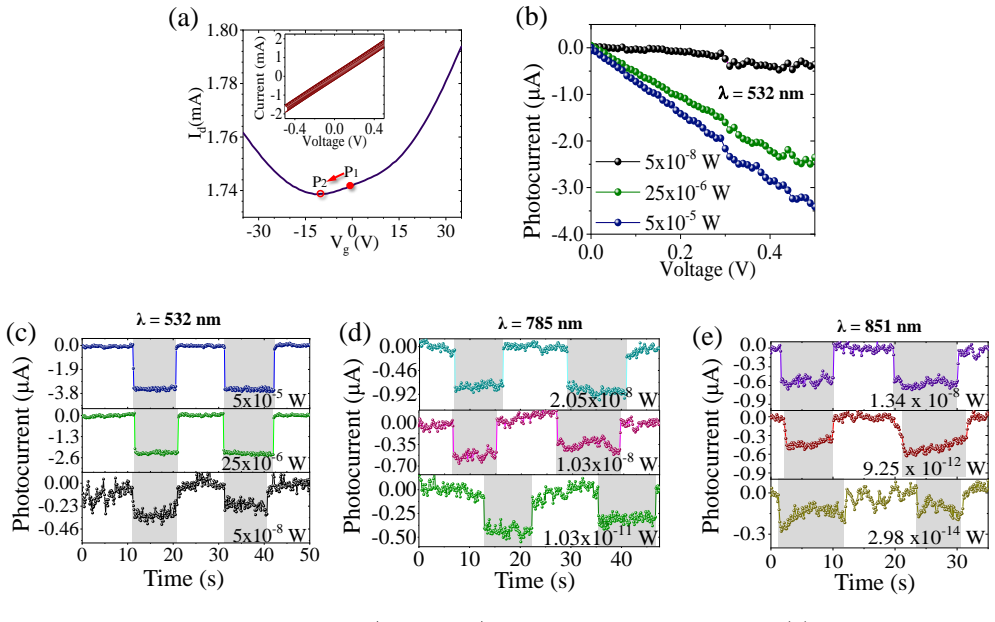
The central discovery is that a floating monolayer MoS2 quantum well, coupled to a few-layer graphene channel through an ultrathin WS2 spacer, produces a quantum-confined photogating effect strong enough to give a measured responsivity of $4.4\times 10^6$ A/W at 30 fW incident power (851 nm) and a noise equivalent power below 4 fW/$\sqrt{\mathrm{Hz}}$, while the built-in band offset discharges the MoS2 rapidly when illumination stops, giving response times under 10 ms with zero reminiscent photocurrent. The paper frames this as the first time a graphene-absorption detector simultaneously achieves ultra-high responsivity, low noise, and fast, self-restoring response at room temperature. A coupled rate-equation model with density-dependent recombination in graphene, interlayer transfer in both directions, and trapping in MoS2 reproduces the measured responsivity over 11 orders of magnitude of incident power density.
Load-bearing premise
The claim depends on the accuracy of the optical power stated as falling on the 6 $\mu$m$^2$ junction; the paper does not report power-meter calibration, beam spot size relative to the junction, or measurement uncertainty, so if the true power at the junction is larger than stated, the responsivity is proportionally lower.
Editorial extensions
If this is right
- Graphene-absorption photodetectors can reach sensitivities that rival detectors with separate absorbing layers, while preserving graphene's broadband absorption from the visible to the near-infrared.
- The automatic discharge mechanism removes the need for the gate-voltage refresh pulses used in earlier photogating detectors, simplifying the system.
- With NEP below 4 fW/$\sqrt{\mathrm{Hz}}$ and response times under 10 ms, the device is practical for room-temperature low-light sensing in the near-infrared.
- Because the responsivity follows a single trend line across 532 to 1050 nm, the photogating mechanism should extend across the full graphene absorption band.
Reading between the lines
- The fitted model's slow de-trapping time ($\tau_{TM} \gg \tau_{MG}$) implies that MoS2 defect states dominate the gain at low power, so engineering the defect density in MoS2 should tune the responsivity; this is a testable prediction.
- At 30 fW with SNR near 10, the device is approaching the few-hundred-photon-per-second regime; whether it can be pushed toward single-photon detection depends on reducing the dark current noise further and on the exact optical power calibration.
- The same floating-quantum-well architecture could be transferred to other transition-metal-dichalcogenide pairs with suitable band offsets, and if graphene remains the absorber, the principle should hold at longer wavelengths than the TMD bandgaps.
- The absolute responsivity values should be read as upper bounds until the optical power at the junction is independently calibrated; the relative comparison across wavelengths is less sensitive to that uncertainty.
Signed reviews
Editorial analysis
A structured set of objections, weighed in public.
Referee Report
Summary. The manuscript reports a vertical FLG/2L-WS2/1L-MoS2 heterojunction photodetector in which photoexcited electrons in few-layer graphene transfer to a monolayer MoS2 quantum well, producing a photogating effect. The authors report a responsivity of 4.4×10^6 A/W at 30 fW incident power at 851 nm, an NEP < 4 fW/√Hz, response times below 10 ms, and no persistent photocurrent. They support the mechanism with temperature-dependent PL quenching measurements and a rate-equation model with fitted parameters.
Significance. If the performance figures are reproducible, the detector would represent a substantial advance over graphene-absorption photodetectors, combining high gain with millisecond-scale response. The PL experiments provide direct evidence of carrier storage in MoS2, and the fabrication of two devices (D1, D2) with consistent behavior is a strength. The principal issue is that the headline responsivity and NEP rest on an uncalibrated optical power value at the junction; until that is documented, the magnitude of the claimed improvement is not verifiable.
major comments (3)
- [§2.4, Fig. 5a and Eq. (6)] The paper does not describe how the 30 fW optical power falling on the 6 µm² junction was determined. The text states only that this is the smallest power 'incident on the junction' during the experiment, with no details of the calibration chain (e.g., attenuator accuracy, beam spot size relative to the junction, power meter traceability). Because R = Iph/Pop and NEP = NRMS/R, any error in Pop propagates linearly into both headline figures; a factor-of-10 underestimate would reduce R to 4.4×10^5 A/W. The authors must provide a complete optical calibration description and an uncertainty estimate.
- [§2.4, Eqs. (1)-(4) and Fig. 5a] The 'model predicted' responsivity curve is obtained by fitting three free parameters (τMG/τGM=10, τMT/τTM=5×10^-4, NT=5×10^10 cm^-2), and the internal quantum efficiency η is not assigned a value. The agreement over 11 orders of magnitude is therefore a demonstration of the model's flexibility, not an independent prediction. The manuscript should either determine these parameters independently or clearly label the curve as a fit and discuss the sensitivity of the conclusion to the fitted values.
- [Fig. 5a and Fig. 5c] None of the measured responsivity or SNR data points carry error bars, and the NEP of <4 fW/√Hz is derived from a single SNR measurement (SNR≈10 at 30 fW). The authors should provide repeated measurements or a statistical uncertainty analysis to support the stated performance margins.
minor comments (5)
- [Throughout] The term 'reminiscent photocurrent' is used; the standard term is 'persistent photocurrent'.
- [§2.4, Eq. (4)] The text says 'Plank constant'; it should be 'Planck constant'.
- [Fig. 5a and Fig. 5c] The x-axis of Fig. 5a is 'Power Density (W/m^2)' while Fig. 5c and the text use 'Power (W)'; the conversion between the two, based on the 6 µm² junction area, should be stated explicitly.
- [§2.3] The exclusion of direct sub-bandgap absorption in MoS2/WS2 is argued from noise and transient response; a direct measurement such as photocurrent excitation spectroscopy below the bandgap would strengthen this conclusion.
- [§2.3, Fig. 4c-e] The rise and fall times are reported as <10 ms and stated to be limited by the measurement equipment; the bandwidth of the measurement setup should be specified to make this bound meaningful.
Circularity Check
Partial circularity: the rate-equation 'model predicted' responsivity in Fig. 5a is a three-parameter fit to the same measured R(Pop) curve; the headline 4.4e6 A/W responsivity is a direct measurement and remains independent, though its optical-power calibration is undocumented.
-
fitted input called prediction
[Section 2.4 'Performance evaluation, modeling, and benchmarking', Eqs. (1)-(4) and Fig. 5a caption]
"The orange curve is the simulated responsivity with fitting parameters τMG/τGM = 10, τMT/τTM = 5×10⁻⁴, and NT = 5×10^10 cm-2. ... The simulated results follow the experimentally obtained R remarkably well over 11 orders of magnitude of incident optical power density."
The three parameters (τMG/τGM, τMT/τTM, NT) are the fitting knobs of Eq. (4). Once they are tuned to the measured R-versus-power data, evaluating Eq. (4) on the same power axis and calling the result 'model predicted responsivity' (Fig. 5a caption) presents a fit as a prediction. The 11-order agreement is a statement about the fit quality, not about an independent forecast. This does not affect the direct experimental R = Iph/Pop, which is measured rather than derived, so the circularity is confined to the model-validation narrative.
full rationale
The central empirical claims—4.4×10^6 A/W responsivity at 30 fW, NEP < 4 fW/√Hz, and millisecond response—are direct measurements of photocurrent and quoted optical power, not outputs of the rate-equation model. The only load-bearing reduction-by-construction is in Section 2.4: the model described by Eqs. (1)-(4) uses fitted ratios τMG/τGM = 10, τMT/τTM = 5×10⁻⁴, and NT = 5×10^10 cm−2, and the resulting orange curve is labeled 'model predicted.' Since the parameters were chosen to reproduce the measured R(Pop), the claimed 11-order-of-magnitude agreement is a fit-quality statement, not a prediction. There is no significant self-citation load-bearing chain: the cited prior Majumdar-group work (Ref. 53) is used for exciton binding energy modulation and is not central to the photodetector claim. A separate concern is the undocumented optical power calibration at the junction: because R and NEP are inversely proportional to Pop, a factor-of-10 error in the stated 30 fW would collapse the headline responsivity. This is an experimental correctness risk, not a circularity of the derivation chain. Overall score reflects the partial circularity of the model-validation claim while the empirical device result remains independent.
Assumptions & free parameters
free parameters (4)
- τMG/τGM =
10
- τMT/τTM =
5×10^-4
- NT =
5×10^10 cm^-2
- η =
not stated (likely assumed 1)
assumptions (4)
- domain assumption Rate equations in Eq. (1)-(3) with linear transfer and a single trap level capture the device physics.
- domain assumption Ultrafast inter-layer electron transfer from graphene to MoS2 occurs before recombination in graphene.
- domain assumption In steady state, there is no net charge flow between graphene and MoS2 because MoS2 is a floating gate.
- ad hoc to paper Sub-bandgap excitation does not directly excite defects in MoS2/WS2, and the low noise and fast response rule out such absorption.
Cite this review
Pith. "Pith review of Highly Sensitive, Fast Graphene Photodetector with Responsivity $>10^6$ A/W Using Floating Quantum Well Gate." pith.science (2026). https://pith.science/paper/NTGZ4E7G
@misc{pith2026190806924,
  author       = {Pith},
  title        = {Pith review of: Highly Sensitive, Fast Graphene Photodetector with Responsivity $>10^6$ A/W Using Floating Quantum Well Gate},
  year         = {2026},
  howpublished = {\url{https://pith.science/paper/NTGZ4E7G}},
  note         = {Machine review of arXiv:1908.06924}
}
abstract
Graphene, owing to its zero bandgap electronic structure, is promising as an absorption material for ultra-wideband photodetection applications. However, graphene-absorption based detectors inherently suffer from poor responsivity due to weak absorption and fast photocarrier recombination, limiting their viability for low intensity light detection. Here we use a graphene/WS$_2$/MoS$_2$ vertical heterojunction to demonstrate a highly sensitive photodetector, where the graphene layer serves dual purpose, namely as the light absorption layer, and also as the carrier conduction channel, thus maintaining the broadband nature of the photodetector. A fraction of the photoelectrons in graphene encounter ultra-fast inter-layer transfer to a floating monolayer MoS$_2$ quantum well providing strong quantum confined photogating effect. The photodetector shows a responsivity of $4.4\times 10^6$ A/W at 30 fW incident power, outperforming photodetectors reported till date where graphene is used as light absorption material by several orders. In addition, the proposed photodetector exhibits an extremely low noise equivalent power ($N\!E\!P$) of $<4$ fW/$\sqrt{Hz}$ and a fast response ($\sim$ milliseconds) with zero reminiscent photocurrent. The findings are attractive towards the demonstration of graphene-based highly sensitive, fast, broadband photodetection technology.
Figures


Figures from the paper (2 more)

Reference graph
Works this paper leans on
-
[1]
Tan, C. L.; Mohseni, H. Emerging Technologies for High Performance Infrared Detectors. Nanophotonics 2018, 7, 169--197
work page 2018
-
[2]
New Concepts in Infrared Photodetector Designs
Martyniuk, P.; Antoszewski, J.; Martyniuk, M.; Faraone, L.; Rogalski, A. New Concepts in Infrared Photodetector Designs. Applied Physics Reviews 2014, 1, 041102
work page 2014
-
[3]
Downs, C.; Vandervelde, T. E. Progress in Infrared Photodetectors Since 2000. Sensors 2013, 13, 5054--5098
work page 2000
-
[4]
Potter, R. F.; Eisenman, W. L. Infrared Photodetectors: A Review of Operational Detectors. Applied Optics 1962, 1, 567--574
work page 1962
-
[5]
Recent Progress in Infrared Detector Technologies
Rogalski, A. Recent Progress in Infrared Detector Technologies. Infrared Physics and Technology 2011, 54, 136--154
work page 2011
-
[6]
Craig, A. P.; Thompson, M. D.; Tian, Z. B.; Krishna, S.; Krier, A.; Marshall, A. R. InAsSb-Based nBn Photodetectors: Lattice Mismatched Growth on GaAs and Low-Frequency Noise Performance. Semiconductor Science and Technology 2015, 30, 105011(7pp)
work page 2015
-
[7]
Gu, Y.; Zhou, L.; Zhang, Y.; Chen, X.; Ma, Y.; Xi, S.; Li, H. Dark Current Suppression in Metamorphic In _ 0.83 Ga _ 0.17 As Photodetectors with In _ 0.66 Ga _ 0.34 As/InAs Superlattice Electron Barrier. Applied Physics Express 2015, 8, 022202
work page 2015
-
[8]
PbS Colloidal Quantum Dot Photodetectors Operating in the Near Infrared
De Iacovo , A.; Venettacci, C.; Colace, L.; Scopa, L.; Foglia, S. PbS Colloidal Quantum Dot Photodetectors Operating in the Near Infrared. Scientific Reports 2016, 6, 37913
work page 2016
Show all 63 references
-
[9]
Y.; Paradee, G.; Lewis, B
Cui, D.; Xu, J.; Xu, S. Y.; Paradee, G.; Lewis, B. A.; Gerhold, M. D. Infrared Photodiode Based on Colloidal PbSe Nanocrystal Quantum Dots. IEEE Transactions on Nanotechnology 2006, 5, 362--367
2006
-
[10]
J.; Buckle, L.; Gordon, N
Hall, D. J.; Buckle, L.; Gordon, N. T.; Giess, J.; Hails, J. E.; Cairns, J. W.; Lawrence, R. M.; Graham, A.; Hall, R. S.; Maltby, C.; Ashley, T. High-Performance Long-Wavelength HgCdTe Infrared Detectors Grown on Silicon Substrates. Applied Physics Letters 2004, 85, 2113--2115
2004
-
[11]
Progress, Challenges, and Opportunities for HgCdTe Infrared Materials and Detectors
Lei, W.; Antoszewski, J.; Faraone, L. Progress, Challenges, and Opportunities for HgCdTe Infrared Materials and Detectors. Applied Physics Reviews 2015, 2, 041303
2015
-
[12]
F.; Ju, L.; Wang, F.; Heinz, T
Mak, K. F.; Ju, L.; Wang, F.; Heinz, T. F. Optical Spectroscopy of Graphene: From the Far Infrared to the Ultraviolet. Solid State Communications 2012, 152, 1341--1349
2012
-
[13]
M.; Valdes-Garcia, A.; Avouris, P
Xia, F.; Mueller, T.; Lin, Y. M.; Valdes-Garcia, A.; Avouris, P. Ultrafast Graphene Photodetector. Nature Nanotechnology 2009, 4, 839--843
2009
-
[14]
Imaging of Photocurrent Generation and Collection in Single-Layer Graphene 2009
Park, J.; Ruiz-vargas, C. Imaging of Photocurrent Generation and Collection in Single-Layer Graphene 2009. Nano Letters 2009, 9, 1742--1746
2009
-
[15]
M.; Song, J
Gabor, N. M.; Song, J. C. W.; Ma, Q.; Nair, N. L.; Taychatanapat, T.; Watanabe, K.; Taniguchi, T.; Levitov, L. S.; Jarillo-Herrero, P. Hot Carrier–Assisted Intrinsic Photoresponse in Graphene. Science 2011, 334, 648--653
2011
-
[16]
M.; Schrenk, W.; Strasser, G.; Mueller, T
Furchi, M.; Urich, A.; Pospischil, A.; Lilley, G.; Unterrainer, K.; Detz, H.; Klang, P.; Andrews, A. M.; Schrenk, W.; Strasser, G.; Mueller, T. Microcavity-Integrated Graphene Photodetector. Nano Letters 2012, 12, 2773--2777
2012
-
[17]
R.; Blake, P.; Grigorenko, A
Nair, R. R.; Blake, P.; Grigorenko, A. N.; Novoselov, K. S.; Booth, T.; Stauber, T.; Peres, N.; Geim, A. K. Fine Structure Constant Defines Visual Transparency of Graphene. Science 2008, 320, 1308
2008
-
[18]
George, P.; Strait, J.; Dawlaty, J.; Shivaraman, S.; Chandrashekhar, M.; Rana, F.; Spencer, M. G. Ultrafast Optical-Pump Terahertz-Probe Spectroscopy of the Carrier Relaxation and Recombination Dynamics in Epitaxial Graphene. Nano Lett 2008, 8, 4248--4251
2008
-
[19]
A.; Strait, J
Rana, F.; George, P. A.; Strait, J. H.; Dawlaty, J.; Shivaraman, S.; Chandrashekhar, M.; Spencer, M. G. Carrier Recombination and Generation Rates for Intravalley and Intervalley Phonon Scattering in Graphene. Physical Review B 2009, 79, 115447
2009
-
[20]
Graphene Photodetectors for High-Speed Optical Communications
Mueller, T.; Xia, F.; Avouris, P. Graphene Photodetectors for High-Speed Optical Communications. Nature Photonics 2010, 4, 297--301
2010
-
[21]
J.; Kim, Y
Yoo, T. J.; Kim, Y. J.; Lee, S. K.; Kang, C. G.; Chang, K. E.; Hwang, H. J.; Revannath, N.; Lee, B. H. Zero-Bias Operation of CVD Graphene Photodetector with Asymmetric Metal Contacts. ACS Photonics 2018, 5, 365--370
2018
-
[22]
H.; Ferrari, A
Sassi, U.; Parret, R.; Nanot, S.; Bruna, M.; Borini, S.; De Fazio , D.; Zhao, Z.; Lidorikis, E.; Koppens, F. H.; Ferrari, A. C.; Colli, A. Graphene-Based Mid-Infrared Room-Temperature Pyroelectric Bolometers with Ultrahigh Temperature Coefficient of Resistance. Nature Communic...
2017
-
[23]
Increased Responsivity of Suspended Graphene Photodetectors
Freitag, M.; Low, T.; Avouris, P. Increased Responsivity of Suspended Graphene Photodetectors. Nano Letters 2013, 13, 1644--1648
2013
-
[24]
L.; Lombardo, A.; Bruna, M.; Ferrari, A
Spirito, D.; Coquillat, D.; De Bonis , S. L.; Lombardo, A.; Bruna, M.; Ferrari, A. C.; Pellegrini, V.; Tredicucci, A.; Knap, W.; Vitiello, M. S. High Performance Bilayer-Graphene Terahertz Detectors. Applied Physics Letters 2014, 104, 061111
2014
-
[25]
K.; Ho, H
Chen, Z.; Cheng, Z.; Wang, J.; Wan, X.; Shu, C.; Tsang, H. K.; Ho, H. P.; Xu, J. B. High Responsivity, Broadband, and Fast Graphene/Silicon Photodetector in Photoconductor Mode. Advanced Optical Materials 2015, 3, 1207--1214
2015
-
[26]
E.; Yoo, T
Chang, K. E.; Yoo, T. J.; Kim, C.; Kim, Y. J.; Lee, S. K.; Kim, S. Y.; Heo, S.; Kwon, M. G.; Lee, B. H. Gate-Controlled Graphene–Silicon Schottky Junction Photodetector. Small 2018, 14, 1801182
2018
-
[27]
J.; Liu, Y.; Zhou, H.; Yin, A.; Li, Z.; Huang, Y.; Duan, X
Yu, W. J.; Liu, Y.; Zhou, H.; Yin, A.; Li, Z.; Huang, Y.; Duan, X. Highly Efficient Gate-Tunable Photocurrent Generation in Vertical Heterostructures of Layered Materials. Nature Nanotechnology 2013, 8, 952--958
2013
-
[28]
Wan, X. et al. A Self-Powered High-Performance Graphene/Silicon Ultraviolet Photodetector with Ultra-Shallow Junction: Breaking the Limit of Silicon? npj 2D Materials and Applications 2017, 1, 4
2017
-
[29]
Hybrid Graphene Tunneling Photoconductor with Interface Engineering Towards Fast Photoresponse and High Responsivity
Tao, L.; Chen, Z.; Li, X.; Yan, K.; Xu, J.-B. Hybrid Graphene Tunneling Photoconductor with Interface Engineering Towards Fast Photoresponse and High Responsivity. npj 2D Materials and Applications 2017, 1, 19
2017
-
[30]
H.; Chang, Y
Liu, C. H.; Chang, Y. C.; Norris, T. B.; Zhong, Z. Graphene Photodetectors with Ultra-Broadband and High Responsivity at Room Temperature. Nature Nanotechnology 2014, 9, 273--278
2014
-
[31]
Konstantatos, G.; Badioli, M.; Gaudreau, L.; Osmond, J.; Bernechea, M.; De Arquer , F. P. G.; Gatti, F.; Koppens, F. H. Hybrid Graphene-Quantum Dot Phototransistors with Ultrahigh Gain. Nature Nanotechnology 2012, 7, 363--368
2012
-
[32]
P.; Ramalingam, G.; Raghavan, S.; Ghosh, A
Roy, K.; Padmanabhan, M.; Goswami, S.; Sai, T. P.; Ramalingam, G.; Raghavan, S.; Ghosh, A. Graphene-MoS _2 Hybrid Structures for Multifunctional Photoresponsive Memory Devices. Nature nanotechnology 2013, 8, 826--830
2013
-
[33]
Near-Infrared Photodetectors Based on MoTe _2 /Graphene Heterostructure with High Responsivity and Flexibility
Yu, W.; Li, S.; Zhang, Y.; Ma, W.; Sun, T.; Yuan, J.; Fu, K.; Bao, Q. Near-Infrared Photodetectors Based on MoTe _2 /Graphene Heterostructure with High Responsivity and Flexibility. Small 2017, 13, 1700268
2017
-
[34]
Highly Responsive and Broadband Photodetectors Based on WS _2 -Graphene Van der Waals Epitaxial Heterostructures
Lan, C.; Li, C.; Wang, S.; He, T.; Zhou, Z.; Wei, D. Highly Responsive and Broadband Photodetectors Based on WS _2 -Graphene Van der Waals Epitaxial Heterostructures. Journal of Materials Chemistry C 2017, 5, 1494--1500
2017
-
[35]
T.; Li, S.; Zhang, T.; Wang, J
Wu, J.-y.; Chun, Y. T.; Li, S.; Zhang, T.; Wang, J. Broadband MoS _2 Field-Effect Phototransistors : Ultrasensitive Visible-Light Photoresponse and Negative Infrared Photoresponse. Advanced Materials 2018,
2018
-
[36]
Broadband Optical-Fiber-Compatible Photodetector with a Synergetic Photogenerating Mechanism
Xiong, Y.-f.; Chen, J.-h.; Lu, Y.-q.; Xu, F. Broadband Optical-Fiber-Compatible Photodetector with a Synergetic Photogenerating Mechanism. Advanced Electronic Materials 2019,
2019
-
[37]
MoS _2 –HgTe Quantum Dot Hybrid Photodetectors beyond 2 µm
Huo, N.; Gupta, S.; Konstantatos, G. MoS _2 –HgTe Quantum Dot Hybrid Photodetectors beyond 2 µm. Advanced Materials 2017, 29, 1606576
2017
-
[38]
D.; Iodice, M.; Coppola, G
Casalino, M.; Russo, R.; Russo, C.; Ciajolo, A.; Gennaro, E. D.; Iodice, M.; Coppola, G. Free-Space Schottky Graphene/Silicon Photodetectors Operating at 2 m. ACS Photonics 2018, 5, 4577--4585
2018
-
[39]
P.; Huang, J
Zhang, W.; Chuu, C. P.; Huang, J. K.; Chen, C. H.; Tsai, M. L.; Chang, Y. H.; Liang, C. T.; Chen, Y. Z.; Chueh, Y. L.; He, J. H.; Chou, M. Y.; Li, L. J. Ultrahigh-Gain Photodetectors Based on Atomically Thin Graphene-MoS _2 Heterostructures. Scientific Reports 2015, 4, 3826
2015
-
[40]
A.; Sinha, R.; Karabiyik, M.; Das, S.; Choi, W.; Pala, N
Vabbina, P.; Choudhary, N.; Chowdhury, A. A.; Sinha, R.; Karabiyik, M.; Das, S.; Choi, W.; Pala, N. Highly Sensitive Wide Bandwidth Photodetector Based on Internal Photoemission in CVD Grown p-Type MoS _2 /Graphene Schottky Junction. ACS Applied Materials and Interfaces 2015, ...
2015
-
[41]
A.; Lau, S
Sun, Z.; Liu, Z.; Li, J.; Tai, G. A.; Lau, S. P.; Yan, F. Infrared Photodetectors Based on CVD-Grown Graphene and PbS Quantum Dots with Ultrahigh Responsivity. Advanced Materials 2012, 24, 5878--5883
2012
-
[42]
High-Responsivity Photodetectors Based on Formamidinium Lead Halide Perovskite Quantum Dot-Graphene Hybrid
Pan, R.; Li, H.; Wang, J.; Jin, X.; Li, Q.; Wu, Z.; Gou, J.; Jiang, Y.; Song, Y. High-Responsivity Photodetectors Based on Formamidinium Lead Halide Perovskite Quantum Dot-Graphene Hybrid. Particle and Particle Systems Characterization 2018, 35, 1700304
2018
-
[43]
H.; Liu, S
Chang, P. H.; Liu, S. Y.; Lan, Y. B.; Tsai, Y. C.; You, X. Q.; Li, C. S.; Huang, K. Y.; Chou, A. S.; Cheng, T. C.; Wang, J. K.; Wu, C. I. Ultrahigh Responsivity and Detectivity Graphene-Perovskite Hybrid Phototransistors by Sequential Vapor Deposition. Scientific Reports 2017,...
2017
-
[44]
F.; Liu, Z.; Gao, F.; Yan, F
Li, J.; Yuan, S.; Tang, G.; Li, G.; Liu, D.; Li, J.; Hu, X.; Liu, Y.; Li, J.; Yang, Z.; Liu, S. F.; Liu, Z.; Gao, F.; Yan, F. High-Performance, Self-Powered Photodetectors Based on Perovskite and Graphene. ACS Applied Materials and Interfaces 2017, 9, 42779--42787
2017
-
[45]
Y.; Liu, T.; Meng, B.; Li, X.; Liang, G.; Hu, X.; Wang, Q
Zhang, B. Y.; Liu, T.; Meng, B.; Li, X.; Liang, G.; Hu, X.; Wang, Q. J. Broadband High Photoresponse from Pure Monolayer Graphene Photodetector. Nature Communications 2013, 4, 1811
2013
-
[46]
S.; Fan, Y.; Chen, Q.; Tweedie, M.; Wang, X.; Zhou, Y.; Warner, J
Tan, H.; Xu, W.; Sheng, Y.; Lau, C. S.; Fan, Y.; Chen, Q.; Tweedie, M.; Wang, X.; Zhou, Y.; Warner, J. H. Lateral Graphene-Contacted Vertically Stacked WS _2 /MoS _2 Hybrid Photodetectors with Large Gain. Advanced Materials 2019, 1702917, 1--8
2019
-
[47]
G.; Reserbat-Plantey, A.; Watanabe, K.; Taniguchi, T.; Tielrooij, K
Massicotte, M.; Schmidt, P.; Vialla, F.; Sch \" a dler, K. G.; Reserbat-Plantey, A.; Watanabe, K.; Taniguchi, T.; Tielrooij, K. J.; Koppens, F. H. Picosecond Photoresponse in Van der Waals Heterostructures. Nature Nanotechnology 2016, 11, 42--46
2016
-
[48]
Ultrafast Charge Transfer in Atomically Thin MoS _2 /WS _2 Heterostructures
Hong, X.; Kim, J.; Shi, S.-F.; Zhang, Y.; Jin, C.; Sun, Y.; Tongay, S.; Wu, J.; Zhang, Y.; Wang, F. Ultrafast Charge Transfer in Atomically Thin MoS _2 /WS _2 Heterostructures. Nature Nanotechnology 2014, 9, 682--686
2014
-
[49]
M.; Zhuang, W.; Zhang, G.; Zheng, J
Chen, H.; Wen, X.; Zhang, J.; Wu, T.; Gong, Y.; Zhang, X.; Yuan, J.; Yi, C.; Lou, J.; Ajayan, P. M.; Zhuang, W.; Zhang, G.; Zheng, J. Ultrafast Formation of Interlayer Hot Excitons in Atomically Thin MoS _2 /WS _2 Heterostructures. Nature Communications 2016, 7, 12512
2016
-
[50]
A.; Raja, A.; Chernikov, A.; Roquelet, C.; Heinz, T
Hill, M.; F., R. A.; Raja, A.; Chernikov, A.; Roquelet, C.; Heinz, T. F. Exciton Broadening in WS _2 Graphene Heterostructures. Physical Review B 2017, 96, 205401
2017
-
[51]
Strong Photoluminescence Enhancement of MoS _2 through Defect Engineering and Oxygen Bonding
Nan, H.; Wang, Z.; Wang, W.; Liang, Z.; Lu, Y.; Chen, Q.; He, D.; Tan, P.; Miao, F.; Wang, X.; Wang, J.; Ni, Z. Strong Photoluminescence Enhancement of MoS _2 through Defect Engineering and Oxygen Bonding. ACS Nano 2014, 8, 5738--5745
2014
-
[52]
M.; Bradley, A
Ugeda, M. M.; Bradley, A. J.; Shi, S.-F.; da Jornada, F. H.; Zhang, Y.; Qiu, D. Y.; Ruan, W.; Mo, S.-K.; Hussain, Z.; Shen, Z.-X.; Wang, F.; Louie, S. G.; Crommie, M. F. Giant Bandgap Renormalization and Excitonic Effects in a Monolayer Transition Metal Dichalcogenide Semicond...
2014
-
[53]
Direct Observation of Giant Binding Energy Modulation of Exciton Complexes in Monolayer MoSe _2
Gupta, G.; Kallatt, S.; Majumdar, K. Direct Observation of Giant Binding Energy Modulation of Exciton Complexes in Monolayer MoSe _2 . Physical Review B 2017, 96, 081403
2017
-
[54]
R.; Arora, A.; Nogajewski, K.; Slobodeniuk, A
Koperski, M.; Molas, M. R.; Arora, A.; Nogajewski, K.; Slobodeniuk, A. O.; Faugeras, C.; Potemski, M. Optical Properties of Atomically Thin Transition Metal Dichalcogenides: Observations and Puzzles. Nanophotonics 2017, 6, 1289--1308
2017
-
[55]
G.; Christianen, P
Plechinger, G.; Nagler, P.; Arora, A.; Schmidt, R.; Chernikov, A.; del \' A guila, A. G.; Christianen, P. C.; Bratschitsch, R.; Sch \" u ller, C.; Korn, T. Trion Fine Structure and Coupled Spin–Valley Dynamics in Monolayer Tungsten Disulfide. Nature Communications 2016, 7, 12715
2016
-
[56]
V.; Mitioglu, A
Nagler, P.; Ballottin, M. V.; Mitioglu, A. A.; Durnev, M. V.; Taniguchi, T.; Watanabe, K.; Chernikov, A.; Sch \" u ller, C.; Glazov, M. M.; Christianen, P. C. M.; Korn, T. Zeeman Splitting and Inverted Polarization of Biexciton Emission in Monolayer WS _2 . Physical Review Let...
2018
-
[57]
O.; Faugeras, C.; Potemski, M.; Molas, M
Vaclavkova, D.; Wyzula, J.; Nogajewski, K.; Bartos, M.; Slobodeniuk, A. O.; Faugeras, C.; Potemski, M.; Molas, M. R. Singlet and Triplet Trions in WS _2 Monolayer Encapsulated in Hexagonal Boron Nitride. Nanotechnology 2018, 29, 325705
2018
-
[58]
Electron-Hole Generation and Recombination Rates for Coulomb Scattering in Graphene
Rana, F. Electron-Hole Generation and Recombination Rates for Coulomb Scattering in Graphene. Physical Review B 2007, 76, 155431
2007
-
[59]
Y.; Waltl, M.; Schanovsky, F.; Stampfer, B.; Furchi, M
Knobloch, T.; Rzepa, G.; Illarionov, Y. Y.; Waltl, M.; Schanovsky, F.; Stampfer, B.; Furchi, M. M.; Mueller, T.; Grasser, T. A Physical Model for the Hysteresis in MoS _2 Transistors. IEEE Journal of the Electron Devices Society 2018, 6, 972--978
2018
-
[60]
M.; Polyushkin, D
Furchi, M. M.; Polyushkin, D. K.; Pospischil, A.; Mueller, T. Mechanisms of Photoconductivity in Atomically Thin MoS _2 . Nano Letters 2014, 14, 6165--6170
2014
-
[61]
https://www.thorlabs.com/images/TabImages/Noise \_ Equivalent \_ Power \_ White \_ Paper.pdf NEP – Noise Equivalent Power
Mackowiak, V.; Jens, P.; Ma, Y.; Gorges, A. https://www.thorlabs.com/images/TabImages/Noise \_ Equivalent \_ Power \_ White \_ Paper.pdf NEP – Noise Equivalent Power . 2007; https://www.thorlabs.com/images/TabImages/Noise \_ Equivalent \_ Power \_ White \_ Paper.pdf
2007
-
[62]
Plasmonically Enhanced Graphene Photodetector Featuring 100 GBd , High-Responsivity and Compact Size
Ma, P.; Salamin, Y.; Baeuerle, B.; Josten, A.; Heni, W. Plasmonically Enhanced Graphene Photodetector Featuring 100 GBd , High-Responsivity and Compact Size. ACS Photonics 2018,
2018
-
[63]
QcQ[r ^ܸD' 1'\\/6'KQ 1B=ᅦB 5-lv[ 4
Freitag, M.; Low, T.; Xia, F.; Avouris, P. Photoconductivity of Biased Graphene. Nature Photonics 2013, 7, 53--59 mcitethebibliography manuscript.tex0000664000000000000000000012470513526550301012476 0ustar rootroot [journal=aamick,manuscript=article] achemso chemformula [T1] f...
2013
Reviewed August 14, 2026 · model on record in the stance chip above.
Discussion (0). Continue with ORCID to comment.