Near-Field Characterisation of Guided Modes in WS2 Nanobeams and Quasi-Bulk Crystals
Pith reviewed 2026-07-02 07:16 UTC · model grok-4.3
The pith
Hyperspectral cavity-enhanced imaging sets bounds on WS2 extinction while s-SNOM maps mode-specific dispersion and loss in its waveguides from 800-1400 nm.
A machine-rendered reading of the paper's core claim, the machinery that carries it, and where it could break.
Core claim
Hyperspectral cavity-enhanced imaging determines high-resolution upper and lower bounds on the extinction coefficient of WS2 within the visible-NIR edge, while s-SNOM measurements of TE0, TM0 and higher-order modes in quasi-bulk and nanobeam WS2 waveguides across 800-1400 nm identify mode-specific trends in wavevector dispersion and loss; s-SNOM supplies upper bounds on propagation loss and relative modal trends despite geometry dependence, and nanobeam data contain artefacts from transverse interference that can shift extracted effective indices by up to 0.25.
What carries the argument
scattering-type scanning near-field optical microscopy (s-SNOM) together with hyperspectral cavity-enhanced imaging to isolate material extinction from waveguide loss channels.
If this is right
- Tighter extinction bounds narrow the predicted range of modal decay lengths for WS2-based integrated circuits.
- Mode-specific dispersion and loss trends guide selection of TE versus TM operation in anisotropic WS2 waveguides.
- s-SNOM can be used as a diagnostic that supplies upper bounds on loss and relative modal trends for other anisotropic van der Waals waveguides.
- Artefacts from transverse interference must be corrected when extracting effective indices from nanobeams whose width approaches the excitation wavelength.
Where Pith is reading between the lines
- The reported bounds could reduce uncertainty in wafer-scale yield estimates when WS2 is integrated with silicon photonic circuits.
- Similar s-SNOM surveys on other transition-metal dichalcogenides might expose common trends in mode confinement versus layer thickness.
- Accounting for spatial sampling effects could extend accurate effective-index extraction to sub-wavelength nanobeam devices.
Load-bearing premise
Cavity-enhanced imaging and s-SNOM geometry can separate intrinsic material extinction from other loss channels, interference and sampling effects sufficiently to yield reliable bounds.
What would settle it
A direct cut-back measurement of propagation loss in a long, straight WS2 waveguide whose value lies outside the extinction-derived upper and lower limits reported from the cavity data.
Figures
read the original abstract
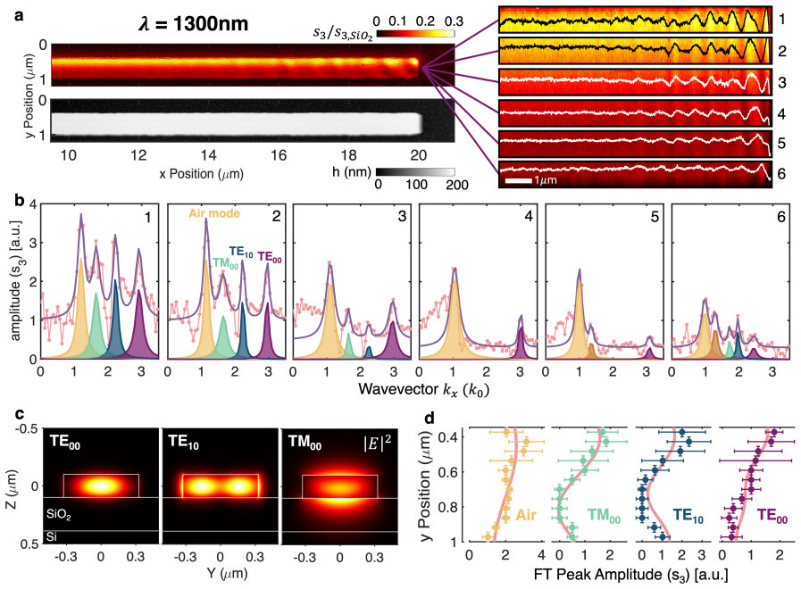
The exceptionally high in-plane refractive index, low sub-bandgap absorption, and strong optical anisotropy of WS2 make it a promising material platform for next-generation integrated circuits for nanophotonics. Its layered van der Waals structure further enables heterogeneous integration with silicon photonics and emerging two-dimensional optoelectronic materials. However, despite increasing interest in the waveguiding properties of WS2, experimental studies of wavelength-dependent modal confinement and attenuation remain limited. Additionally, though the extinction coefficient of WS2 is expected to be near-negligible beneath the bandgap, reported values span orders of magnitude, leading to large uncertainty in predicted modal decay lengths and wafer-scale integration feasibility. To resolve these ambiguities we perform hyperspectral cavity-enhanced imaging, determining high-resolution upper and lower bounds on the extinction coefficient of WS2 within the visible-NIR edge. We further employ scattering-type scanning near-field optical microscopy (s-SNOM) to probe TE0, TM0, and higher-order modes in both quasi-bulk and nanobeam WS2 waveguides across the 800-1400 nm spectral range, enabling identification of mode-specific trends in wavevector dispersion and loss. This work simultaneously assesses s-SNOM as a probe of waveguide performance, and we find that while absolute loss values depend on measurement geometry, s-SNOM reliably captures relative modal trends and provides upper bounds on propagation loss, supporting its use as a diagnostic tool for anisotropic waveguides. We further identify significant artefacts in nanobeam measurements arising from transverse interference and spatial sampling effects when the structure size approaches the excitation wavelength, which can shift extracted effective indices by up to 0.25.
Editorial analysis
A structured set of objections, weighed in public.
Referee Report
Summary. The paper reports experimental measurements on WS2 nanobeams and quasi-bulk crystals using hyperspectral cavity-enhanced imaging to establish high-resolution upper and lower bounds on the sub-bandgap extinction coefficient in the visible-NIR range, combined with s-SNOM characterization of TE0, TM0 and higher-order guided modes across 800-1400 nm to extract wavevector dispersion and loss trends, while explicitly noting geometry-dependent artefacts that can shift effective indices by up to 0.25 and framing absolute loss values as geometry-specific rather than intrinsic material constants.
Significance. If the extinction bounds and relative modal trends hold after improved quantification, the work would reduce uncertainty in WS2 waveguide design for nanophotonics integration, provide a practical diagnostic role for s-SNOM on anisotropic structures, and supply falsifiable experimental constraints on sub-bandgap absorption that are currently reported over orders of magnitude in the literature.
major comments (3)
- [Methods/Results] Methods and Results sections: the central claim of high-resolution upper/lower bounds on the extinction coefficient via cavity-enhanced imaging lacks accompanying sample-thickness metrology, full error propagation, or raw hyperspectral data traces, making independent verification of the separation between material extinction and cavity/interface losses impossible from the presented information.
- [s-SNOM results] s-SNOM analysis (800-1400 nm range): the statement that absolute loss values depend on geometry while relative trends remain reliable is load-bearing for the diagnostic-tool conclusion, yet the manuscript provides no quantitative comparison (e.g., cross-geometry loss ratios or simulated vs. measured dispersion shifts) to substantiate that the 0.25 effective-index artefact does not also affect the reported mode-specific loss trends.
- [Abstract/Discussion] Abstract and discussion: the weakest assumption—that cavity-enhanced imaging and s-SNOM geometries sufficiently isolate material extinction from interference and scattering channels—is not tested with a control experiment or sensitivity analysis, which directly limits in the reported bounds.
minor comments (3)
- [Figures] Figure captions and axis labels should explicitly state the number of independent samples or spatial locations averaged for each dispersion/loss datum.
- [Notation] Notation for effective index and propagation loss should be introduced consistently in the text before first use in figures.
- [Discussion] A brief comparison table of the new extinction bounds against the range of literature values would improve readability.
Simulated Author's Rebuttal
We thank the referee for their constructive and detailed comments, which highlight important areas for strengthening the manuscript's rigor and verifiability. We address each major comment point-by-point below. Where the comments identify gaps in supporting information or analysis, we have incorporated revisions to address them directly.
read point-by-point responses
-
Referee: [Methods/Results] Methods and Results sections: the central claim of high-resolution upper/lower bounds on the extinction coefficient via cavity-enhanced imaging lacks accompanying sample-thickness metrology, full error propagation, or raw hyperspectral data traces, making independent verification of the separation between material extinction and cavity/interface losses impossible from the presented information.
Authors: We agree that these details are necessary for independent verification. In the revised manuscript, we have added AFM-based sample thickness metrology to the Methods section, included a complete error propagation analysis (accounting for cavity losses, interface effects, and measurement uncertainties) in the Supplementary Information, and provided raw hyperspectral data traces as new supplementary figures. These additions enable readers to assess the separation of material extinction from other loss channels. revision: yes
-
Referee: [s-SNOM results] s-SNOM analysis (800-1400 nm range): the statement that absolute loss values depend on geometry while relative trends remain reliable is load-bearing for the diagnostic-tool conclusion, yet the manuscript provides no quantitative comparison (e.g., cross-geometry loss ratios or simulated vs. measured dispersion shifts) to substantiate that the 0.25 effective-index artefact does not also affect the reported mode-specific loss trends.
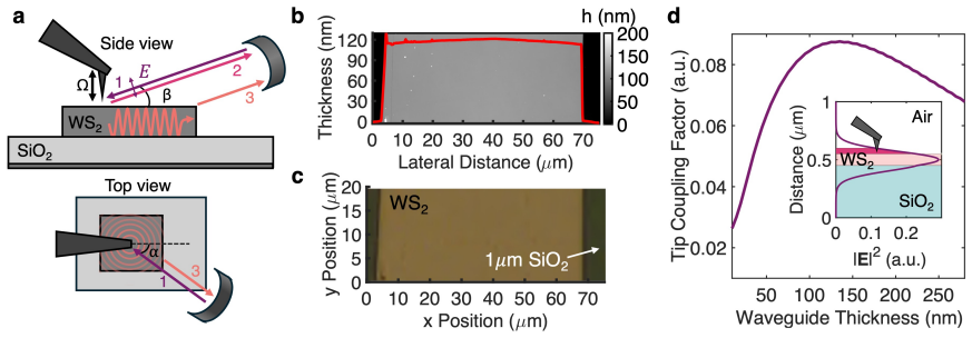
Authors: We acknowledge the need for quantitative substantiation of the relative trends. The revised manuscript includes a new subsection with cross-geometry loss ratios derived from both experimental data and finite-element simulations, along with direct comparisons of simulated versus measured dispersion shifts. These demonstrate that the 0.25 effective-index artefact impacts absolute values but preserves the relative ordering and trends in mode-specific losses, supporting the diagnostic utility of s-SNOM. revision: yes
-
Referee: [Abstract/Discussion] Abstract and discussion: the weakest assumption—that cavity-enhanced imaging and s-SNOM geometries sufficiently isolate material extinction from interference and scattering channels—is not tested with a control experiment or sensitivity analysis, which directly limits in the reported bounds.
Authors: This is a fair critique of the isolation assumption. A dedicated control experiment would require additional sample sets not available within the current study scope. However, we have added a sensitivity analysis in the revised Discussion quantifying the impact of interference and scattering channels on the extracted bounds. We have also revised the Abstract and Discussion to more explicitly qualify the bounds as geometry-constrained and to note the sensitivity results, thereby tempering the claims appropriately. revision: partial
Circularity Check
No significant circularity
full rationale
The paper is a purely experimental study reporting direct measurements via hyperspectral cavity-enhanced imaging for extinction bounds and s-SNOM for waveguide modes. No derivation chain, fitted parameters presented as predictions, self-citations as load-bearing uniqueness theorems, or ansatzes exist. All claims reduce to observed data without internal reduction to inputs by construction.
Axiom & Free-Parameter Ledger
Reference graph
Works this paper leans on
-
[1]
Davis, Daniel E
Timothy J. Davis, Daniel E. G´ omez, and Ann Roberts. Plasmonic circuits for manipulating optical informa- tion.Nanophotonics, 6(3):543–559, 2017
2017
-
[2]
M.A. Butt, B. Janaszek, and R. Piramidowicz. Lighting the way forward: The bright future of photonic integrated circuits.Sensors International, 6:100326, 2025
2025
-
[3]
Bowers, Alexis Bjorlin, Robert Blum, and John E
Near Margalit, Chao Xiang, Steven M. Bowers, Alexis Bjorlin, Robert Blum, and John E. Bowers. Perspective on the future of silicon photonics and electronics.Applied Physics Letters, 118(22):220501, 06 2021
2021
-
[4]
Electricity demand and grid impacts of AI data centers: Challenges and prospects, 2025
Xin Chen, Xiaoyang Wang, Ana Colacelli, Matt Lee, and Le Xie. Electricity demand and grid impacts of AI data centers: Challenges and prospects, 2025
2025
-
[5]
Y. Yuan, Y. Peng, S. Cheung, X. Xiao, W. V. Sorin, Z. Huang, D. Liang, A. Kumar, R. Liu, Y. Hu, S. Hooten, S. Palermo, M. Fiorentino, and R. G. Beausoleil. The perspective of all-silicon photonics and systems.APL Photonics, 10(6):060901, 06 2025
2025
-
[6]
Jacob B. Khurgin. Expanding the photonic palette: Exploring high index materials.ACS Photonics, 9(3):743– 751, 03 2022
2022
-
[7]
Hyungki Shim, Zeyu Kuang, and Owen D. Miller. Optical materials for maximal nanophotonic response [invited].Opt. Mater. Express, 10(7):1561–1585, Jul 2020
2020
-
[8]
Sacher, Xianshu Luo, Yisu Yang, Fu-Der Chen, Thomas Lordello, Jason C
Wesley D. Sacher, Xianshu Luo, Yisu Yang, Fu-Der Chen, Thomas Lordello, Jason C. C. Mak, Xinyu Liu, Ting Hu, Tianyuan Xue, Patrick Guo-Qiang Lo, Michael L. Roukes, and Joyce K. S. Poon. Visible-light silicon nitride waveguide devices and implantable neurophotonic probes on thinned 200 mm silicon wafers. Opt. Express, 27(26):37400–37418, Dec 2019
2019
-
[9]
D. E. Aspnes and A. A. Studna. Dielectric functions and optical parameters of Si, Ge, GaP, GaAs, GaSb, InP, InAs, and InSb from 1.5 to 6.0 eV.Phys. Rev. B, 27:985–1009, Jan 1983
1983
-
[10]
Leonid Tsybeskov, D. J. Lockwood, and Masato Ichikawa. Silicon photonics: Cmos going optical [scanning the issue]. 2009
2009
-
[11]
Vlasov and Sharee J
Yurii A. Vlasov and Sharee J. McNab. Losses in single-mode silicon-on-insulator strip waveguides and bends. Opt. Express, 12(8):1622–1631, Apr 2004
2004
-
[12]
Fabrication, characterization and loss analysis of silicon nanowaveguides.J
Chao Qiu, Zhen Sheng, Hao Li, Wei Liu, Le Li, Albert Pang, Aimin Wu, Xi Wang, Shichang Zou, and Fuwan Gan. Fabrication, characterization and loss analysis of silicon nanowaveguides.J. Lightwave Technol., 32(13):2303–2307, Jul 2014
2014
-
[13]
Reboud, A
V. Reboud, A. Gassenq, J.M. Hartmann, J. Widiez, L. Virot, J. Aubin, K. Guilloy, S. Tardif, J.M. F´ ed´ eli, N. Pauc, A. Chelnokov, and V. Calvo. Germanium based photonic components toward a full sil- icon/germanium photonic platform.Progress in Crystal Growth and Characterization of Materials, 63(2):1– 24, June 2017
2017
-
[14]
Kaustubh Vyas, Daniel H. G. Espinosa, Daniel Hutama, Shubhendra Kumar Jain, Rania Mahjoub, Ehsan Mobini, Kashif M. Awan, Jeff Lundeen, and Ksenia Dolgaleva. Group III-V semiconductors as promising nonlinear integrated photonic platforms.Advances in Physics: X, 7(1):2097020, 2022. 15
2022
-
[15]
Kimerling
Jurgen Michel, Jifeng Liu, and Lionel C. Kimerling. High-performance Ge-on-Si photodetectors.Nature Photonics, 4(8):527–534, 2010
2010
-
[16]
Yu. B. Bolkhovityanov and O. P. Pchelyakov. GaAs epitaxy on Si substrates: modern status of research and engineering.Physics-Uspekhi, 51:437 – 456, 2008
2008
-
[17]
Integration of 2D materials on a silicon photonics platform for optoelectronics applications.Nanophotonics, 6(6):1205–1218, 2017
Nathan Youngblood and Mo Li. Integration of 2D materials on a silicon photonics platform for optoelectronics applications.Nanophotonics, 6(6):1205–1218, 2017
2017
-
[18]
Glazov, Tony F
Gang Wang, Alexey Chernikov, Mikhail M. Glazov, Tony F. Heinz, Xavier Marie, Thierry Amand, and Bernhard Urbaszek. Colloquium: Excitons in atomically thin transition metal dichalcogenides.Rev. Mod. Phys., 90:021001, Apr 2018
2018
-
[19]
Yazyev, and Andras Kis
Sajedeh Manzeli, Dmitry Ovchinnikov, Diego Pasquier, Oleg V. Yazyev, and Andras Kis. 2D transition metal dichalcogenides.Nature Reviews Materials, 2(8):17033, 2017
2017
-
[20]
Recent advances in the carrier mobility of two-dimensional materials: A theoretical perspective.ACS Omega, 5(24):14203–14211, 06 2020
Showkat Hassan Mir, Vivek Kumar Yadav, and Jayant Kumar Singh. Recent advances in the carrier mobility of two-dimensional materials: A theoretical perspective.ACS Omega, 5(24):14203–14211, 06 2020
2020
-
[21]
Photo- luminescence from chemically exfoliated MoS2.Nano Letters, 11(12):5111–5116, 12 2011
Goki Eda, Hisato Yamaguchi, Damien Voiry, Takeshi Fujita, Mingwei Chen, and Manish Chhowalla. Photo- luminescence from chemically exfoliated MoS2.Nano Letters, 11(12):5111–5116, 12 2011
2011
-
[22]
Chaves, J
A. Chaves, J. G. Azadani, Hussain Alsalman, D. R. da Costa, R. Frisenda, A. J. Chaves, Seung Hyun Song, Y. D. Kim, Daowei He, Jiadong Zhou, A. Castellanos-Gomez, F. M. Peeters, Zheng Liu, C. L. Hinkle, Sang-Hyun Oh, Peide D. Ye, Steven J. Koester, Young Hee Lee, Ph. Avouris, Xinran Wang, and Tony Low. Bandgap engineering of two-dimensional semiconductor m...
2020
-
[23]
Polyakov, Maria Bancerek, Tomasz J
George Zograf, Alexander Yu. Polyakov, Maria Bancerek, Tomasz J. Antosiewicz, Bet¨ ul K¨ u¸ c¨ uk¨ oz, and Timur O. Shegai. Combining ultrahigh index with exceptional nonlinearity in resonant transition metal dichalcogenide nanodisks.Nature Photonics, 18(7):751–757, 2024
2024
-
[24]
2D materials for optical modulation: Challenges and opportunities.Advanced Materials, 29(14):1606128, 2017
Shaoliang Yu, Xiaoqin Wu, Yipei Wang, Xin Guo, and Limin Tong. 2D materials for optical modulation: Challenges and opportunities.Advanced Materials, 29(14):1606128, 2017
2017
-
[25]
Recent advances in 2D materials for photodetectors.Advanced Electronic Materials, 7(7):2001125, 2021
Jian Jiang, Yao Wen, Hao Wang, Lei Yin, Ruiqing Cheng, Chuansheng Liu, Liping Feng, and Jun He. Recent advances in 2D materials for photodetectors.Advanced Electronic Materials, 7(7):2001125, 2021
2021
-
[26]
Bright and efficient light-emitting devices based on 2D transition metal dichalcogenides.Advanced Materials, 35(31):2208054, 2023
Tanveer Ahmed, Jiajia Zha, Kris KH Lin, Hao-Chung Kuo, Chaoliang Tan, and Der-Hsien Lien. Bright and efficient light-emitting devices based on 2D transition metal dichalcogenides.Advanced Materials, 35(31):2208054, 2023
2023
-
[27]
Teresa L´ opez-Carrasco and Marcos H. D. Guimar˜ aes. Atomically thin transition metal dichalcogenide nanolasers: Challenges and opportunities.Applied Physics Letters, 126(22), June 2025
2025
-
[28]
Ermolaev, Dmitry I
Georgy A. Ermolaev, Dmitry I. Yakubovsky, Yury V. Stebunov, Aleksey V. Arsenin, and Valentyn S. Volkov. Spectral ellipsometry of monolayer transition metal dichalcogenides: Analysis of excitonic peaks in dispersion. Journal of Vacuum Science & Technology B, 38(1):014002, 12 2019
2019
-
[29]
Panaiot G. Zotev, Yue Wang, Daniel Andres-Penares, Toby Severs-Millard, Sam Randerson, Xuerong Hu, Luca Sortino, Charalambos Louca, Mauro Brotons-Gisbert, Tahiyat Huq, Stefano Vezzoli, Riccardo Sapienza, Thomas F. Krauss, Brian D. Gerardot, and Alexander I. Tartakovskii. Van der waals materials for applica- tions in nanophotonics.Laser and Photonics Revie...
2023
-
[30]
Antosiewicz, and Timur O
Battulga Munkhbat, Piotr Wr´ obel, Tomasz J. Antosiewicz, and Timur O. Shegai. Optical constants of several multilayer transition metal dichalcogenides measured by spectroscopic ellipsometry in the 300–1700 nm range: High index, anisotropy, and hyperbolicity.ACS Photonics, 9(7):2398–2407, 07 2022
2022
-
[31]
Giant opti- cal anisotropy of WS2 flakes in the visible region characterized by au substrate assisted near-field optical microscopy.Nanotechnology, 33(34):345201, 2022
Nan Deng, Hua Long, Kun Wang, Xiaobo Han, Bing Wang, Kai Wang, and Peixiang Lu. Giant opti- cal anisotropy of WS2 flakes in the visible region characterized by au substrate assisted near-field optical microscopy.Nanotechnology, 33(34):345201, 2022
2022
-
[32]
Ultrathin WS2 polariton waveguide for efficient light guiding.Advanced Optical Materials, 11(16):2300069, 2023
Seong Won Lee, Jong Seok Lee, Woo Hun Choi, and Su-Hyun Gong. Ultrathin WS2 polariton waveguide for efficient light guiding.Advanced Optical Materials, 11(16):2300069, 2023
2023
-
[33]
Anisotropic slot waveguides with bulk transition metal dichalcogenides for crosstalk reduction and high-efficiency mode conversion.Optics Express, 30(17):30219–30232, 2022
Chia-Chien Huang. Anisotropic slot waveguides with bulk transition metal dichalcogenides for crosstalk reduction and high-efficiency mode conversion.Optics Express, 30(17):30219–30232, 2022
2022
-
[34]
Vyshnevyy, Georgy A
Andrey A. Vyshnevyy, Georgy A. Ermolaev, Dmitriy V. Grudinin, Kirill V. Voronin, Ivan Kharichkin, Arslan Mazitov, Ivan A. Kruglov, Dmitry I. Yakubovsky, Prabhash Mishra, Roman V. Kirtaev, Aleksey V. Arsenin, Kostya S. Novoselov, Luis Martin-Moreno, and Valentyn S. Volkov. van der waals materials for overcoming fundamental limitations in photonic integrate...
2023
-
[35]
Reduction in crosstalk between integrated anisotropic optical waveguides.Photonics, 10(1):59, 2023
Dmitriy Grudinin, Olga Matveeva, Georgy Ermolaev, Andrey Vyshnevyy, Aleksey Arsenin, and Valentyn Volkov. Reduction in crosstalk between integrated anisotropic optical waveguides.Photonics, 10(1):59, 2023
2023
-
[36]
Broadband angular dispersion compensation for digital micromirror devices.Optics Letters, 47(3):457–460, 2022
Dihan Chen, Bingxu Chen, Qi Shao, and Shih-Chi Chen. Broadband angular dispersion compensation for digital micromirror devices.Optics Letters, 47(3):457–460, 2022
2022
-
[37]
IntechOpen, London, 2015
David S´ anchez Montero, Carmen V´ azquez Garc´ ıa, Plinio Jes´ us Pinz´ on Castillo, Alberto Tapetado Moraleda, Pedro Contreras Lallana, and Isabel P´ erez Garcil´ opez.Recent Advances in Wavelength-Division-Multiplexing Plastic Optical Fiber Technologies. IntechOpen, London, 2015
2015
-
[38]
Nonvolatile photonic switch with magnetic materials on a silicon photonic platform [invited].Optical Materials Express, 13(9):2489–2496, 2023
Yuya Shoji, Shohei Taniguchi, and Shun Yajima. Nonvolatile photonic switch with magnetic materials on a silicon photonic platform [invited].Optical Materials Express, 13(9):2489–2496, 2023
2023
-
[39]
Coupling strategies for silicon photonics integrated chips [invited].Photonics Research, 7(2):201–239, 2019
Riccardo Marchetti, Cosimo Lacava, Lee Carroll, Kamil Gradkowski, and Paolo Minzioni. Coupling strategies for silicon photonics integrated chips [invited].Photonics Research, 7(2):201–239, 2019
2019
-
[40]
Temperature-dependent dispersion model of float zone crystalline silicon.Applied Surface Science, 421:405– 419, 2017
Daniel Franta, Adam Dubroka, Chennan Wang, Angelo Giglia, Jir´ ı Voh´ anka, Pavel Franta, and Ivan Ohl´ ıdal. Temperature-dependent dispersion model of float zone crystalline silicon.Applied Surface Science, 421:405– 419, 2017
2017
-
[41]
Sternbach, Daniel J
Fabian Mooshammer, Sanghoon Chae, Shuai Zhang, Yinming Shao, Siyuan Qiu, Anjaly Rajendran, Aaron J. Sternbach, Daniel J. Rizzo, Xiaoyang Zhu, P. James Schuck, James C. Hone, and D. N. Basov. In-plane anisotropy in biaxial res2 crystals probed by nano-optical imaging of waveguide modes.ACS Photonics, 9(2):443–451, 02 2022
2022
-
[42]
Visible to mid-infrared giant in-plane optical anisotropy in ternary van der waals crystals
Yanze Feng, Runkun Chen, Junbo He, Liujian Qi, Yanan Zhang, Tian Sun, Xudan Zhu, Weiming Liu, Weiliang Ma, Wanfu Shen, Chunguang Hu, Xiaojuan Sun, Dabing Li, Rongjun Zhang, Peining Li, and Shaojuan Li. Visible to mid-infrared giant in-plane optical anisotropy in ternary van der waals crystals. Nature Communications, 14(1):6739, 2023
2023
-
[43]
G. A. Ermolaev, D. V. Grudinin, Y. V. Stebunov, K. V. Voronin, V. G. Kravets, J. Duan, A. B. Mazitov, G. I. Tselikov, A. Bylinkin, D. I. Yakubovsky, S. M. Novikov, D. G. Baranov, A. Y. Nikitin, I. A. Kruglov, 17 T. Shegai, P. Alonso-Gonz´ alez, A. N. Grigorenko, A. V. Arsenin, K. S. Novoselov, and V. S. Volkov. Giant optical anisotropy in transition metal...
2021
-
[44]
Gilbert Corder, Jianing Chen, Zhipei Sun, Mengkun Liu, and Qing Dai
Debo Hu, Xiaoxia Yang, Chi Li, Ruina Liu, Ziheng Yao, Hai Hu, Stephanie N. Gilbert Corder, Jianing Chen, Zhipei Sun, Mengkun Liu, and Qing Dai. Probing optical anisotropy of nanometer-thin van der waals microcrystals by near-field imaging.Nature Communications, 8(1):1471, 2017
2017
-
[45]
I. H. Malitson. Interspecimen comparison of the refractive index of fused silica*,†.Journal of the Optical Society of America, 55(10):1205–1209, 1965
1965
-
[46]
Roughness induced backscattering in optical silicon waveguides.Phys
Francesco Morichetti, Antonio Canciamilla, Carlo Ferrari, Matteo Torregiani, Andrea Melloni, and Mario Martinelli. Roughness induced backscattering in optical silicon waveguides.Phys. Rev. Lett., 104:033902, Jan 2010. 18 Supplementary Notes iCEAS Imaging Cavity-Enhanced Absorption Spectroscopy (iCEAS) is applied to produce hyperspectral extinction maps of...
2010
-
[47]
An additional global loss of 150 ppm is applied within calculation of these finesse values to account for scattering due to residue left behind during the TMD exfoliation process
are used to isolate crystal absorption. An additional global loss of 150 ppm is applied within calculation of these finesse values to account for scattering due to residue left behind during the TMD exfoliation process. With Asp thus extracted, this can be related to extinctionκvia the Beer-Lambert law, wherein intensity loss due to crystal absorption is ...
discussion (0)
Sign in with ORCID, Apple, or X to comment. Anyone can read and Pith papers without signing in.