Vanadium superconducting microwave resonators on silicon wafers
Pith reviewed 2026-07-02 10:02 UTC · model grok-4.3
The pith
Losses in vanadium superconducting resonators are dominated by non-TLS mechanisms at the surface that a tantalum capping layer can reduce.
A machine-rendered reading of the paper's core claim, the machinery that carries it, and where it could break.
Core claim
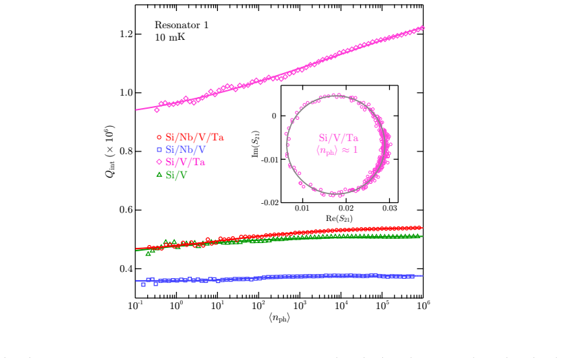
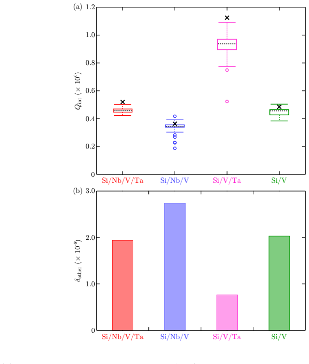
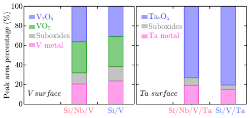
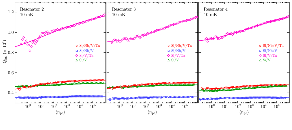
Loss at the V surface is dominated by ⟨n_ph⟩-independent non-two-level-system (non-TLS) losses, which can be mitigated by introducing the Ta capping layer. The V films on the Nb buffer layers exhibit lower Q_int and higher non-TLS loss than that directly grown on Si wafers, even though the former has higher lattice-orientation uniformity. Origins of these trends might be relevant to V oxides and/or V hydrides at surfaces and grain boundaries.
What carries the argument
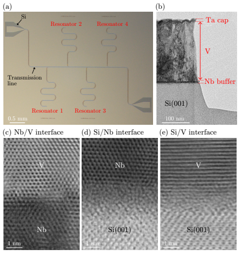
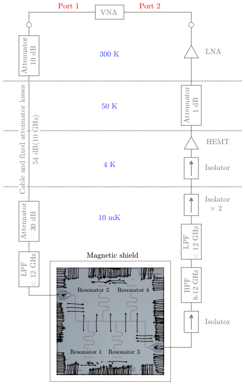
The photon-number dependence of internal quality factor Q_int in resonators made from four different V-film stacks (Nb/V/Ta, Nb/V, V/Ta, V), used to separate TLS and non-TLS loss contributions.
If this is right
- Introducing a Ta capping layer mitigates non-TLS losses in V resonators.
- Nb buffer layers increase non-TLS loss in V films compared to direct growth on Si.
- Better lattice orientation uniformity does not guarantee lower losses in these V films.
- V oxides or hydrides at surfaces and grain boundaries are likely sources of the non-TLS losses.
- Mitigation strategies should target surface chemistry rather than just improving crystallinity.
Where Pith is reading between the lines
- Vanadium could serve as an alternative material for quantum circuits if surface losses are controlled.
- Similar capping strategies might apply to other superconducting films prone to oxide formation.
- Direct growth without buffers may be preferable for V on Si to minimize additional loss channels.
- Further studies could test hydride formation by varying processing conditions.
Load-bearing premise
The performance differences between film stacks are caused by V oxides or hydrides at surfaces and grain boundaries rather than by differences in interface quality or measurement artifacts.
What would settle it
Measuring resonators from V films where EDX and XPS show no oxides or hydrides but still finding the same differences in Q_int and non-TLS loss between Nb-buffered and direct-growth samples would falsify the proposed origin.
Figures
read the original abstract
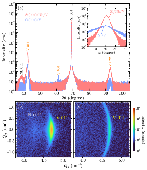
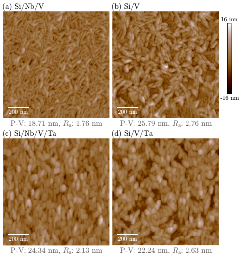
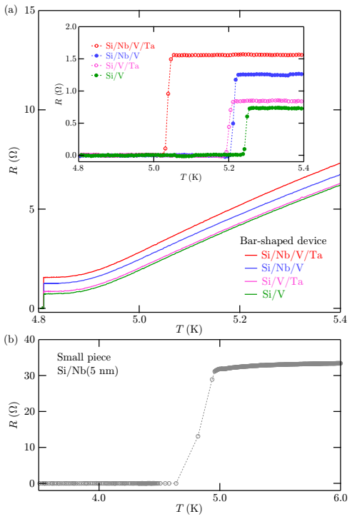
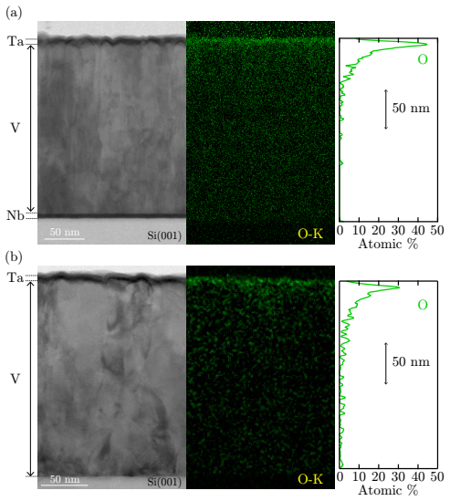
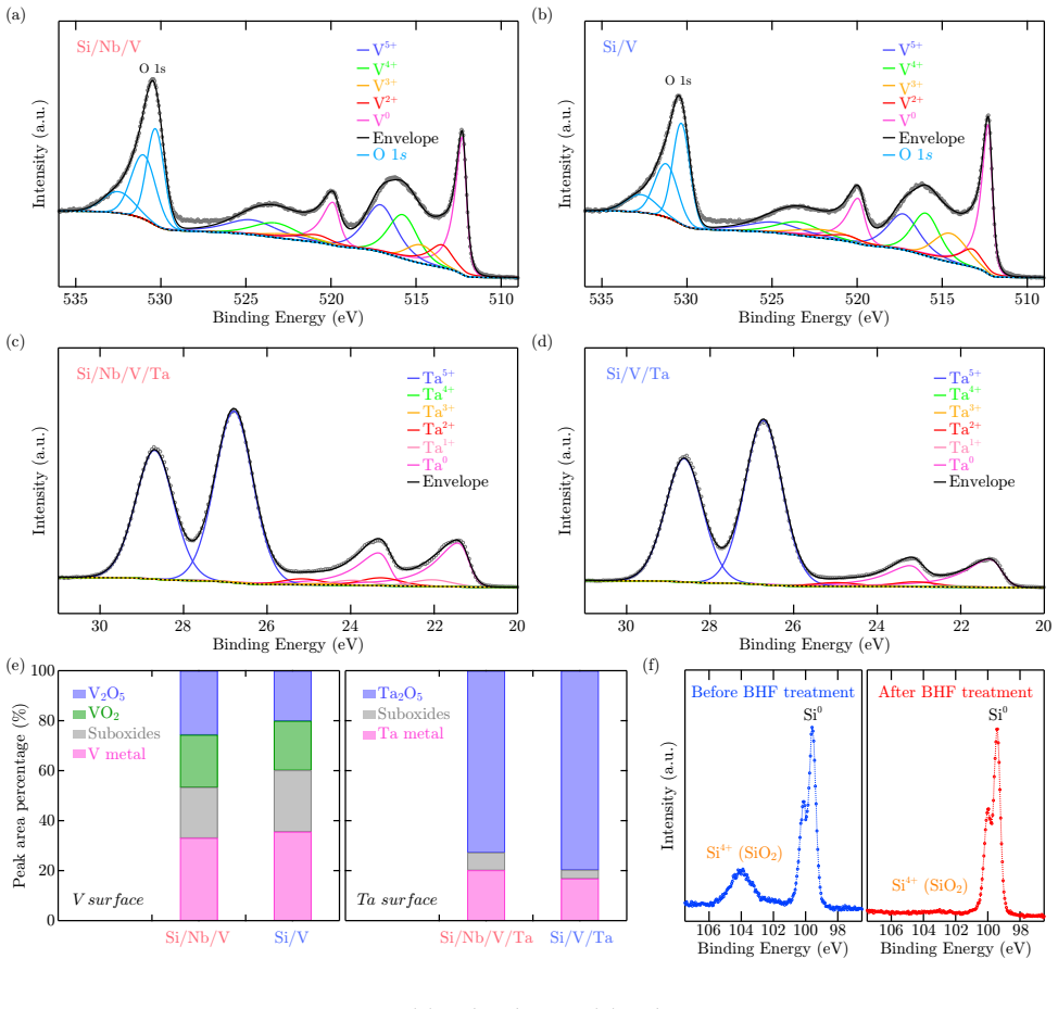
Understanding the correlation between material properties and microwave losses in superconducting films is a crucial subject for developing low-loss materials for quantum circuits. We focus on vanadium (V) as a novel material for superconducting quantum devices and discuss loss in V films in relation to their structural properties. Using a sputtering method, we grow four V-film structures on (001)-oriented Si wafers, employing Nb and Ta as the buffer and capping layer materials, respectively: Nb/V/Ta, Nb/V, V/Ta, and V. X-ray diffraction and atomic force microscopy reveal that the V films grown on the Nb buffer layers have higher uniformity of lattice orientation and smaller grain size than that directly grown on the Si wafer. Coplanar waveguide resonators are fabricated from the four V-film structures, and averaged photon number ($\langle n_{\rm ph} \rangle$) dependences of internal quality factor ($Q_{\rm int}$) are obtained by performing microwave measurements. By analyzing the obtained $Q_{\rm int}$ vs $\langle n_{\rm ph} \rangle$, it is found that loss at the V surface is dominated by $\langle n_{\rm ph} \rangle$-independent non-two-level-system (non-TLS) losses, which can be mitigated by introducing the Ta capping layer. Furthermore, the V films on the Nb buffer layers exhibit lower $Q_{\rm int}$ in the $\langle n_{\rm ph} \rangle$ range from 10$^{0}$ to 10$^{6}$ and higher non-TLS loss than that directly grown on Si wafers, even though the former has higher lattice-orientation uniformity than the latter. Origins of these trends might be relevant to V oxides, of which presence at surfaces and grain boundaries in bulk regions in the V resonators is suggested by energy dispersive X-ray spectroscopy and X-ray photoelectron spectroscopy, and/or V hydrides.
Editorial analysis
A structured set of objections, weighed in public.
Referee Report
Summary. The manuscript reports fabrication and microwave characterization of coplanar waveguide resonators from four vanadium film structures (Nb/V/Ta, Nb/V, V/Ta, V) sputtered on Si(001). XRD and AFM show Nb-buffered films have superior lattice-orientation uniformity and smaller grains. Q_int versus <n_ph> measurements indicate that V-surface losses are dominated by <n_ph>-independent non-TLS mechanisms that are reduced by Ta capping; Nb-buffered films nevertheless show lower Q_int (10^0 to 10^6 photons) and higher non-TLS loss than direct V/Si films, with EDX/XPS suggesting V oxides or hydrides at surfaces and grain boundaries as a possible origin.
Significance. If the non-TLS dominance and Ta-mitigation claims are confirmed with quantitative controls, the work would supply concrete guidance on surface-chemistry engineering for low-loss vanadium resonators in quantum circuits, separating structural uniformity from chemical-loss contributions.
major comments (3)
- [Abstract / Q_int vs <n_ph> analysis] Abstract and results on Q_int(<n_ph>) analysis: the claim that non-TLS losses dominate and are higher in Nb-buffered films rests on post-measurement fitting whose details (functional form, error bars, number of resonators per structure, exclusion criteria for outlier devices) are not supplied, preventing independent evaluation of the extracted non-TLS loss coefficients.
- [Discussion of origins of trends] Discussion of Nb-buffer versus direct-growth contrast: the inference that elevated non-TLS loss originates from V oxides/hydrides (detected by EDX/XPS) lacks any quantitative correlation between oxide/hydride areal density or depth profile and the reported non-TLS loss rates; no controls isolating this from Nb/V interface scattering, film stress, or post-etch contamination are described.
- [Results / loss-parameter table] Table or figure presenting Q_int and non-TLS loss values: without tabulated values, uncertainties, or statistical tests for the four structures, the statement that Nb/V films exhibit “higher non-TLS loss” cannot be assessed for magnitude or significance.
minor comments (2)
- Notation for average photon number is inconsistent between <n_ph> and ⟨n_ph⟩; standardize throughout.
- EDX and XPS spectra or depth profiles should be shown with quantitative elemental percentages rather than qualitative “presence suggested.”
Simulated Author's Rebuttal
We thank the referee for the careful reading and constructive comments. We address each major point below. Where details were omitted, we will add them in revision; where inferences are suggestive rather than quantitative, we will clarify the limitations of the data.
read point-by-point responses
-
Referee: [Abstract / Q_int vs <n_ph> analysis] Abstract and results on Q_int(<n_ph>) analysis: the claim that non-TLS losses dominate and are higher in Nb-buffered films rests on post-measurement fitting whose details (functional form, error bars, number of resonators per structure, exclusion criteria for outlier devices) are not supplied, preventing independent evaluation of the extracted non-TLS loss coefficients.
Authors: We agree that the fitting procedure and supporting statistics were not described in sufficient detail. In the revised manuscript we will specify the functional form used to separate TLS and non-TLS contributions, include error bars on all Q_int data points, state the number of resonators measured for each film structure, and document the criteria applied to exclude outlier devices. These additions will enable independent assessment of the extracted non-TLS coefficients. revision: yes
-
Referee: [Discussion of origins of trends] Discussion of Nb-buffer versus direct-growth contrast: the inference that elevated non-TLS loss originates from V oxides/hydrides (detected by EDX/XPS) lacks any quantitative correlation between oxide/hydride areal density or depth profile and the reported non-TLS loss rates; no controls isolating this from Nb/V interface scattering, film stress, or post-etch contamination are described.
Authors: The manuscript already qualifies the link as suggestive (“might be relevant … suggested by”). We will revise the discussion to state explicitly that no quantitative correlation between oxide/hydride density and loss rates has been established, and that other possible contributions (interface scattering, stress, contamination) have not been isolated by dedicated controls. This change will prevent over-interpretation while retaining the EDX/XPS observations as one plausible origin. revision: yes
-
Referee: [Results / loss-parameter table] Table or figure presenting Q_int and non-TLS loss values: without tabulated values, uncertainties, or statistical tests for the four structures, the statement that Nb/V films exhibit “higher non-TLS loss” cannot be assessed for magnitude or significance.
Authors: We will add a table (or expanded figure caption) that reports representative Q_int values at selected photon numbers, the fitted non-TLS loss coefficients with uncertainties, and basic statistical information (mean and standard deviation across devices) for each of the four film structures. This will allow direct evaluation of the magnitude and significance of the reported differences. revision: yes
- We do not possess additional EDX/XPS data that would allow quantitative areal-density or depth-profile correlations with the measured non-TLS loss rates; the existing spectra were acquired for qualitative identification only.
Circularity Check
No circularity: experimental measurements and post-hoc interpretation
full rationale
The paper reports fabrication of four V-film structures, XRD/AFM characterization, resonator fabrication, and direct microwave measurements of Q_int vs ⟨n_ph⟩. Loss analysis separates TLS and non-TLS contributions via standard fitting to measured curves; attributions to oxides/hydrides rest on qualitative EDX/XPS observations rather than any equation that reduces the reported loss rates to fitted inputs by construction. No self-citations, uniqueness theorems, or ansatzes are invoked to force the central claims. The chain consists of independent experimental data and standard loss modeling, making the result self-contained.
Axiom & Free-Parameter Ledger
free parameters (1)
- non-TLS loss coefficient
axioms (1)
- domain assumption The standard model form for two-level-system loss in resonators (power-law or saturating dependence on photon number) applies to these vanadium devices.
Reference graph
Works this paper leans on
-
[1]
M. H. Devoret and R. J. Schoelkopf, Superconducting circuits for quantum information: An outlook, Science339, 1169 (2013)
2013
-
[2]
Kjaergaard, M
M. Kjaergaard, M. E. Schwartz, J. Braum¨ uller, P. Krantz, J. I.-J. Wang, S. Gustavsson, and W. D. Oliver, Superconducting qubits: Current state of play, Annu. Rev. Condens. Matter. Phys.11, 369 (2020)
2020
-
[3]
J. M. Sage, V. Bolkhovsky, W. D. Oliver, B. Turek, and P. B. Welander, Study of loss in superconducting coplanar waveguide resonators, J. Appl. Phys.109, 063915 (2011)
2011
-
[4]
W. D. Oliver and P. B. Welander, Materials in superconducting quantum bits, MRS Bull.38, 816 (2013)
2013
-
[5]
C. R. H. McRae, H. Wang, J. Gao, M. R. Vissers, T. Brecht, A. Dunsworth, D. P. Pappas, and J. Mutus, Materials loss measurements using superconducting microwave resonators, Rev. Sci. Instrum.91, 091101 (2020)
2020
-
[6]
N. P. de Leon, K. M. Itoh, D. Kim, K. K. Mehta, T. E. Northup, H. Paik, B. S. Palmer, N. Samarth, S. Sangtawesin, and D. W. Steuerman, Materials challenges and opportunities for quantum computing hardware, Science372, 253 (2021)
2021
-
[7]
Siddiqi, Engineering high-coherence superconducting qubits, Nat
I. Siddiqi, Engineering high-coherence superconducting qubits, Nat. Rev. Mater.6, 875 (2021)
2021
-
[8]
A. D. O’Connell, M. Ansmann, R. C. Bialczak, M. Hofheinz, N. Katz, E. Lucero, C. McKenney, M. Neeley, H. Wang, E. M. Weig, A. N. Cleland, and J. M. Martinis, Microwave dielectric loss at single photon energies and millikelvin temperatures, Appl. Phys. Lett.92, 112903 (2008)
2008
-
[10]
Megrant, C
A. Megrant, C. Neill, R. Barends, B. Chiaro, Y. Chen, L. Feigl, J. Kelly, E. Lucero, M. Mariantoni, P. J. J. O’Malley, D. Sank, A. Vainsencher, J. Wenner, T. C. White, Y. Yin, J. Zhao, C. J. Palmstrøm, J. M. Martinis, and A. N. Cleland, Planar superconducting res- onators with internal quality factors above one million, Appl. Phys. Lett.100, 113510 (2012)
2012
-
[11]
C. J. K. Richardson, N. P. Siwak, J. Hackley, Z. K. Keane, J. E. Robinson, B. Arey, I. Arslan, and B. S. Palmer, Fabrication artifacts and parallel loss channels in metamorphic epitaxial 28 aluminum superconducting resonators, Supercond. Sci. Technol.29, 064003 (2016)
2016
-
[12]
Dunsworth, A
A. Dunsworth, A. Megrant, C. Quintana, Z. Chen, R. Barends, B. Burkett, B. Foxen, Y. Chen, B. Chiaro, A. Fowler, R. Graff, E. Jeffrey, J. Kelly, E. Lucero, J. Y. Mutus, M. Neeley, C. Neill, P. Roushan, D. Sank, A. Vainsencher,et al., Characterization and reduction of capacitive loss induced by sub-micron Josephson junction fabrication in superconducting q...
2017
-
[13]
Gr¨ unhaupt, N
L. Gr¨ unhaupt, N. Maleeva, S. T. Skacel, M. Calvo, F. Levy-Bertrand, A. V. Ustinov, H. Rotzinger, A. Monfardini, G. Catelani, and I. M. Pop, Loss mechanisms and quasiparti- cle dynamics in superconducting microwave resonators made of thin-film granular aluminum, Phys. Rev. Lett.121, 117001 (2018)
2018
-
[14]
C. T. Earnest, J. H. B´ ejanin, T. G. McConkey, E. A. Peters, A. Korinek, H. Yuan, and M. Mariantoni, Substrate surface engineering for high-quality silicon/aluminum supercon- ducting resonators, Supercond. Sci. Technol.31, 125013 (2018)
2018
-
[15]
S. Un, S. de Graaf, P. Bertet, S. Kubatkin, and A. Danilov, On the nature of decoherence in quantum circuits: Revealing the structural motif of the surface radicals inα-Al 2O3, Sci. Adv. 8, eabm6169 (2022)
2022
-
[16]
Kumar, J
S. Kumar, J. Gao, J. Zmuidzinas, B. A. Mazin, H. G. LeDuc, and P. K. Day, Temperature dependence of the frequency and noise of superconducting coplanar waveguide resonators, Appl. Phys. Lett.92, 123503 (2008)
2008
-
[17]
Macha, S
P. Macha, S. H. W. van der Ploeg, G. Oelsner, E. Il’ichev, H.-G. Meyer, S. W¨ unsch, and M. Siegel, Losses in coplanar waveguide resonators at millikelvin temperatures, Appl. Phys. Lett.96, 062503 (2010)
2010
-
[18]
Burnett, L
J. Burnett, L. Faoro, and T. Lindstr¨ om, Analysis of high quality superconducting resonators: consequences for TLS properties in amorphous oxides, Supercond. Sci. Technol.29, 044008 (2016)
2016
-
[19]
J. M. Gambetta, C. E. Murray, Y.-K.-K. Fung, D. T. McClure, O. Dial, W. Shanks, J. W. Sleight, and M. Steffen, Investigating surface loss effects in superconducting transmon qubits, IEEE Trans. Appl. Supercond.27, 1700205 (2016)
2016
-
[20]
Verjauw, A
J. Verjauw, A. Potoˇ cnik, M. Mongillo, R. Acharya, F. Mohiyaddin, G. Simion, A. Pacco, T. Ivanov, D. Wan, A. Vanleenhove, L. Souriau, J. Jussot, A. Thiam, J. Swerts, X. Piao, S. Couet, M. Heyns, B. Govoreanu, and I. Radu, Investigation of microwave loss induced by 29 oxide regrowth in high-Qniobium resonators, Phys. Rev. Applied16, 014018 (2021)
2021
-
[21]
M. V. P. Alto´ e, A. Banerjee, C. Berk, A. Hajr, A. Schwartzberg, C. Song, M. Alghadeer, S. Aloni, M. J. Elowson, J. M. Kreikebaum, E. K. Wong, S. M. Griffin, S. Rao, A. Weber- Bargioni, A. M. Minor, D. I. Santiago, S. Cabrini, I. Siddiqi, and D. F. Ogletree, Localization and mitigation of loss in niobium superconducting circuits, PRX Quantum3, 020312 (2022)
2022
-
[22]
C. G. Torres-Castanedo, D. P. Goronzy, T. Pham, A. McFadden, N. Materise, P. M. Das, M. Cheng, D. Lebedev, S. M. Ribet, M. J. Walker,et al., Formation and microwave losses of hydrides in superconducting niobium thin films resulting from fluoride chemical processing, Adv. Funct. Mater.34, 2401365 (2024)
2024
-
[23]
Z. Sung, D. Bafia, A. Cano, A. Murthy, J. Lee, M. J. Reagor, J. Rubio-Zuazo, A. Grassellino, and A. Romanenko, Formation of niobium hydride precipitates in superconducting qubits, Phys. Rev. Materials10, 016201 (2026)
2026
-
[24]
A. P. M. Place, L. V. H. Rodgers, P. Mundada, B. M. Smitham, M. Fitzpatrick, Z. Leng, A. Premkumar, J. Bryon, A. Vrajitoarea, S. Sussman,et al., New material platform for super- conducting transmon qubits with coherence times exceeding 0.3 milliseconds, Nat. Commun. 12, 1779 (2021)
2021
-
[25]
C. Wang, X. Li, H. Xu, Z. Li, J. Wang, Z. Yang, Z. Mi, X. Liang, T. Su, C. Yang,et al., Towards practical quantum computers: Transmon qubit with a lifetime approaching 0.5 milliseconds, npj Quantum Inf.8, 3 (2022)
2022
-
[26]
K. D. Crowley, R. A. McLellan, A. Dutta, N. Shumiya, A. P. M. Place, X. H. Le, Y. Gang, T. Madhavan, M. P. Bland, R. Chang,et al., Disentangling losses in tantalum superconducting circuits, Phys. Rev. X13, 041005 (2023)
2023
-
[27]
Urade, K
Y. Urade, K. Yakushiji, M. Tsujimoto, T. Yamada, K. Makise, W. Mizubayashi, and K. Ino- mata, Microwave characterization of tantalum superconducting resonators on silicon substrate with niobium buffer layer, APL Mater.12, 021132 (2024)
2024
-
[28]
D. P. Lozano, M. Mongillo, X. Piao, S. Couet, D. Wan, Y. Canvel, A. M. Vadiraj, T. Ivanov, J. Verjauw, R. Acharya,et al., Low-lossα-tantalum coplanar waveguide resonators on silicon wafers: Fabrication, characterization and surface modification, Mater. Quantum Technol.4, 025801 (2024)
2024
-
[29]
D. P. Lozano, M. Mongillo, B. Raes, Y. Canvel, S. Massar, A. M. Vadiraj, T. Ivanov, R. Acharya, J. V. Damme, J. V. de Vondel,et al., Reversing hydrogen-related loss inα-Ta 30 thin films for quantum device fabrication, Adv. Sci.12, e09244 (2025)
2025
-
[30]
M. R. Vissers, J. Gao, D. S. Wisbey, D. A. Hite, C. C. Tsuei, A. D. Corcoles, M. Steffen, and D. P. Pappas, Low loss superconducting titanium nitride coplanar waveguide resonators, Appl. Phys. Lett.97, 232509 (2010)
2010
-
[31]
S. Ohya, B. Chiaro, A. Megrant, C. Neill, R. Barends, Y. Chen, J. Kelly, D. Low, J. Mutus, P. J. J. O’Malley,et al., Room temperature deposition of sputtered TiN films for supercon- ducting coplanar waveguide resonators, Supercond. Sci. Technol.27, 082602 (2013)
2013
-
[32]
Bruno, G
A. Bruno, G. de Lange, S. Asaad, K. L. van der Enden, N. K. Langford, and L. DiCarlo, Reducing intrinsic loss in superconducting resonators by surface treatment and deep etching of silicon substrates, Appl. Phys. Lett.106, 182601 (2015)
2015
-
[33]
S. E. de Graaf, L. Faoro, J. Burnett, A. A. Adamyan, A. Y. Tzalenchuk, S. E. Kubatkin, T. Lindstr¨ om, and A. V. Danilov, Suppression of low-frequency charge noise in superconduct- ing resonators by surface spin desorption, Nat. Commun.9, 1143 (2018)
2018
-
[34]
S. Kim, H. Terai, T. Yamashita, W. Qiu, T. Fuse, F. Yoshihara, S. Ashhab, K. Inomata, and K. Semba, Enhanced coherence of all-nitride superconducting qubits epitaxially grown on silicon substrate, Commun. Mater.2, 98 (2021)
2021
-
[35]
Premkumar, C
A. Premkumar, C. Weiland, S. Hwang, B. J¨ ack, A. P. M. Place, I. Waluyo, A. Hunt, V. Bisogni, J. Pelliciari, A. Barbour, M. S. Miller, P. Russo, F. Camino, K. Kisslinger, X. Tong, M. S. Hybertsen, A. A. Houck, and I. Jarrige, Microscopic relaxation channels in materials for superconducting qubits, Commun. Mater.2, 72 (2021)
2021
-
[36]
L. D. Alegria, D. M. Tennant, K. R. Chaves, J. R. I. Lee, S. R. O’Kelley, Y. J. Rosen, and J. L. DuBois, Two-level systems in nucleated and non-nucleated epitaxial alpha-tantalum films, Appl. Phys. Lett.123, 062601 (2024)
2024
-
[37]
S. G. Jones, N. Materise, K. W. Leung, J. C. Weber, B. D. Isakov, X. Chen, J. Zheng, A. Gyenis, B. Jaeck, and C. R. H. McRae, Grain size in low loss superconducting Ta thin films on c axis sapphire, J. Appl. Phys.134, 144402 (2023)
2023
-
[38]
M. P. Bland, F. Bahrami, J. G. C. Martinez, P. H. Prestegaard, B. M. Smitham, A. Joshi, E. Hedrick, S. Kumar, A. Yang, A. C. Pakpour-Tabrizi, A. Jindal, R. D. Chang, G. Cheng, N. Yao, R. J. Cava, N. P. de Leon, and A. A. Houck, Millisecond lifetimes and coherence times in 2D transmon qubits, Nature647, 343 (2025)
2025
-
[39]
R. Gao, W. Yu, H. Deng, H.-S. Ku, Z. Li, M. Wang, X. Miao, Y. Lin, and C. Deng, Epi- 31 taxial titanium nitride microwave resonators: structural, chemical, electrical, and microwave properties, Phys. Rev. Materials6, 036202 (2022)
2022
-
[40]
Singer, B
M. Singer, B. Schoof, H. Gupta, D. Zahn, J. Weber, and M. Tornow, Tantalum thin films sput- tered on silicon and on different seed layers: Material characterization and coplanar waveguide resonator performance, in2024 IEEE International Conference on Quantum Computing and Engineering (QCE), Montreal, QC, Canada(2024) p. 1197
2024
-
[41]
T. A. J. van Schijndel, A. P. McFadden, A. N. Engel, J. T. Dong, W. J. Y.-Parre˜ no, M. Parthasarathy, R. W. Simmonds, and C. J. Palmstrøm, Cryogenic growth of tantalum thin films for low-loss superconducting circuits, Phys. Rev. Applied23, 034025 (2025)
2025
-
[42]
Marcaud, D
G. Marcaud, D. Perello, C. Chen, E. Umbarkar, C. Weiland, J. Gao, S. Diez, V. Ly, N. Mahuli, N. D’Souza, Y. He, S. Aghaeimeibodi, R. Resnick, C. Jaye, A. K. Rumaiz, D. A. Fischer, M. Hunt, O. Painter, and I. Jarrige, Low-loss superconducting resonators fabricated from tantalum films grown at room temperature, Commun. Mater.6, 182 (2025)
2025
-
[43]
Dhundhwal, H
R. Dhundhwal, H. Duan, L. Brauch, S. Arabi, D. Fuchs, A.-A. Haghighirad, A. Welle, F. Schar- waechter, S. Pal, M. Scheffler, J. Palomo, Z. Leghtas, A. Murani, H. Hahn, J. Aghassi- Hagmann, C. K¨ ubel, W. Wulfhekel, I. M. Pop, and T. Reisinger, High-quality superconducting tantalum resonators with beta phase defects, Appl. Phys. Lett.127, 214005 (2025)
2025
-
[44]
F. Ando, D. Kan, Y. Shiota, T. Moriyama, Y. Shimakawa, and T. Ono, Fabrication of non- centrosymmetric Nb/V/Ta superlattice and its superconductivity, J. Magn. Soc. Jpn.43, 17 (2019)
2019
-
[45]
F. Ando, Y. Miyasaka, T. Li, J. Ishizuka, T. Arakawa, Y. Shiota, T. Moriyama, Y. Yanase, and T. Ono, Observation of superconducting diode effect, Nature584, 373 (2020)
2020
-
[46]
Radebaugh and P
R. Radebaugh and P. H. Keesom, Low-temperature thermodynamic properties of vanadium. I. superconducting and normal states, Phys. Rev.209, 149 (1966)
1966
-
[47]
Gutsche, H
M. Gutsche, H. Kraus, J. Jochum, B. Kemmather, and G. Gutekunst, Growth and character- ization of epitaxial vanadium films, Thin Solid Films248, 18 (1994)
1994
-
[48]
N. R. Werthamer, Theory of the superconducting transition temperature and energy gap function of superposed metal films, Phys. Rev.132, 2440 (1963)
1963
-
[49]
P. G. de Gennes, Boundary effects in superconductors, Rev. Mod. Phys.36, 225 (1964)
1964
-
[50]
Gonzalez-Arrabal, A
R. Gonzalez-Arrabal, A. Cam´ on, M. Parra-Border´ ıas, L. Fabrega, J. Anguita, J. Ses´ e, and F. Briones, Mo/Au bilayers deposited by sputtering at room temperature for transition edge 32 sensors fabrication, J. Low. Temp. Phys.151, 239 (2008)
2008
-
[51]
J. C. Weber, K. M. Morgan, D. Yan, C. G. Pappas, A. L. Wessels, G. C. O’Neil, D. A. Bennett, G. C. Hilton, D. S. Swetz, J. N. Ullom, and D. R. Schmidt, Development of a transition-edge sensor bilayer process providing new modalities for critical temperature control, Supercond. Sci. Technol.33, 115002 (2020)
2020
-
[52]
D. K. Finnemore, T. F. Stromberg, and C. A. Swenson, Superconducting properties of high- purity niobium, Phys. Rev.149, 231 (1966)
1966
-
[53]
A. F. Mayadas, R. B. Laibowitz, and J. J. Cuomo, Electrical characteristics of rf-sputtered single-crystal niobium films, J. Appl. Phys.43, 1287 (1972)
1972
-
[54]
S. A. Wolf, J. J. Kennedy, and M. Nisenoff, Properties of superconducting rf sputtered ultra- thin films of nb, J. Vac. Sci. Technol.13, 145 (1976)
1976
-
[55]
Kodama, M
J. Kodama, M. Itoh, and H. Hirai, Superconducting transition temperature versus thickness of Nb film on various substrates, J. Appl. Phys.54, 4050 (1983)
1983
-
[56]
M. S. M. Minhaj, S. Meepagala, J. T. Chen, and L. E. Wenger, Thickness dependence on the superconducting properties of thin Nb films, Phys. Rev. B49, 15235 (1994)
1994
-
[57]
M. H. Read and C. Altman, A new structure in tantalum thin films, Appl. Phys. Lett.7, 51 (1965)
1965
-
[58]
Silversmit, D
G. Silversmit, D. Depla, H. Poelman, G. B. Marin, and R. De Gryse, Determination of the V2pXPS binding energies for different vanadium oxidation states (V 5+ to V0+), J. Electron Spectrosc. Relat. Phenom.135, 167 (2004)
2004
-
[59]
M. C. Biesinger, L. W. M. Lau, A. R. Gerson, and R. S. Smart, Resolving surface chemical states in XPS analysis of first row transition metals, oxides and hydroxides: Sc, Ti, V, Cu and Zn, Appl. Surf. Sci.257, 887 (2010)
2010
-
[60]
M. T. Brumbach, P. R. Mickel, A. J. Lohn, A. J. Mirabal, M. A. Kalan, J. E. Stevens, and M. J. Marinella, Evaluating tantalum oxide stoichiometry and oxidation states for optimal memristor performance, J. Vac. Sci. Technol. A32, 051403 (2014)
2014
-
[61]
R. A. McLellan, A. Dutta, C. Zhou, Y. Jia, C. Weiland, X. Gui, A. P. M. Place, K. D. Crowley, X. H. Le, T. Madhavan,et al., Chemical profiles of the oxides on tantalum in state of the art superconducting circuits, Adv. Sci.10, 2300921 (2023)
2023
-
[62]
Bruno, G
A. Bruno, G. de Lange, S. Asaad, K. L. van der Enden, N. K. Langford, and L. DiCarlo, Reducing intrinsic loss in superconducting resonators by surface treatment and deep etching 33 of silicon substrates, Appl. Phys. Lett.106, 182601 (2015)
2015
-
[63]
M. S. Khalil, M. J. A. Stoutimore, F. C. Wellstood, and K. D. Osborn, An analysis method for asymmetric resonator transmission applied to superconducting devices, J. Appl. Phys.111, 054510 (2012)
2012
-
[64]
Geerlings, S
K. Geerlings, S. Shankar, E. Edwards, L. Frunzio, R. J. Schoelkopf, and M. H. Devoret, Improving the quality factor of microwave compact resonators by optimizing their geometrical parameters, Appl. Phys. Lett.100, 192601 (2012)
2012
-
[65]
H. Wang, M. Hofheinz, J. Wenner, M. Ansmann, R. C. Bialczak, M. Lenander, E. Lucero, M. Neeley, A. D. O’Connell, D. Sank, M. Weides, A. N. Cleland, and J. M. Martinis, Improving the coherence time of superconducting coplanar resonators, Appl. Phys. Lett.95, 233508 (2009)
2009
-
[66]
S. S. N. Bharadwaja, C. Venkatasubramanian, N. Fieldhouse, S. Ashok, M. W. Horn, and T. N. Jackson, Low temperature charge carrier hopping transport mechanism in vanadium oxide thin films grown using pulsed dc sputtering, Appl. Phys. Lett.94, 222110 (2009)
2009
-
[67]
A. K. Singh, S. Kumari, H. K. Singh, and P. K. Siwach, Substrate-induced modulation of metal-insulator transition and low-temperature charge transport in radio frequency sputtered VO2 films, Thin Solid Films826, 140773 (2025)
2025
-
[68]
Suzuki, H
T. Suzuki, H. Namazue, S. Koike, and H. Hayakawa, Superdiffusion of 4T-hydrogen in vana- dium, Phys. Rev. Lett.51, 798 (1983)
1983
-
[69]
Luo, H.-B
J. Luo, H.-B. Zhou, Y.-L. Liu, L.-J. Gui, S. Jin, Y. Zhang, and G.-H. Lu, Dissolution, diffusion and permeation behavior of hydrogen in vanadium: a first-principles investigation, J. Phys.: Condens. Matter23, 135501 (2011)
2011
-
[70]
D. R. Courtney,Thermal conductivity of hydrogen doped high purity vanadium, M.S. thesis, Iowa State University, Ames, Iowa, USA (1977)
1977
-
[71]
Li and F
X. Li and F. Peng, Superconductivity of pressure-stabilized vanadium hydrides, Inorg. Chem. 56, 13759 (2017)
2017
-
[72]
Pan and E
Y. Pan and E. Yu, Theoretical prediction of structure, electronic and optical properties of VH2 hydrogen storage material, Int. J. Hydrogen Energy47, 27608 (2022). 34
2022
discussion (0)
Sign in with ORCID, Apple, or X to comment. Anyone can read and Pith papers without signing in.