Phase Stable Integrated Delay Line Asymmetric Mach Zehnder Interferometers Enabled by High Efficiency 3 dB Couplers for Chip Scale QKD
Pith reviewed 2026-06-26 13:18 UTC · model grok-4.3
The pith
A silicon nitride asymmetric Mach-Zehnder interferometer delivers 500 ps delays with visibility above 0.99 for chip-scale QKD receivers.
A machine-rendered reading of the paper's core claim, the machinery that carries it, and where it could break.
Core claim
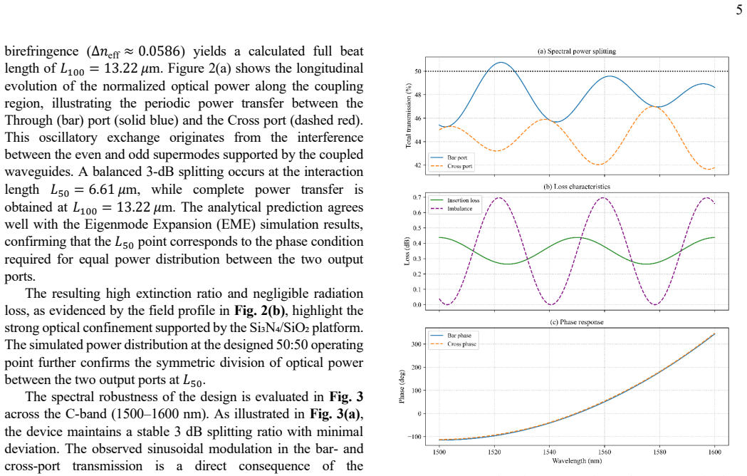
An optimized Si3N4/SiO2 aMZI architecture with high-efficiency 3 dB couplers provides a 500 ps optical delay corresponding to a 2 GHz free spectral range. The structure maintains nearly constant group delay with sub-10 ps variation over 190-200 THz, a smooth near-linear phase response, and stable 3 dB power splitting with insertion loss below 0.5 dB. This enables interference visibility above 0.99 and an estimated QBER below 0.5 percent for gigahertz-rate time-bin QKD while remaining compatible with WDM architectures.
What carries the argument
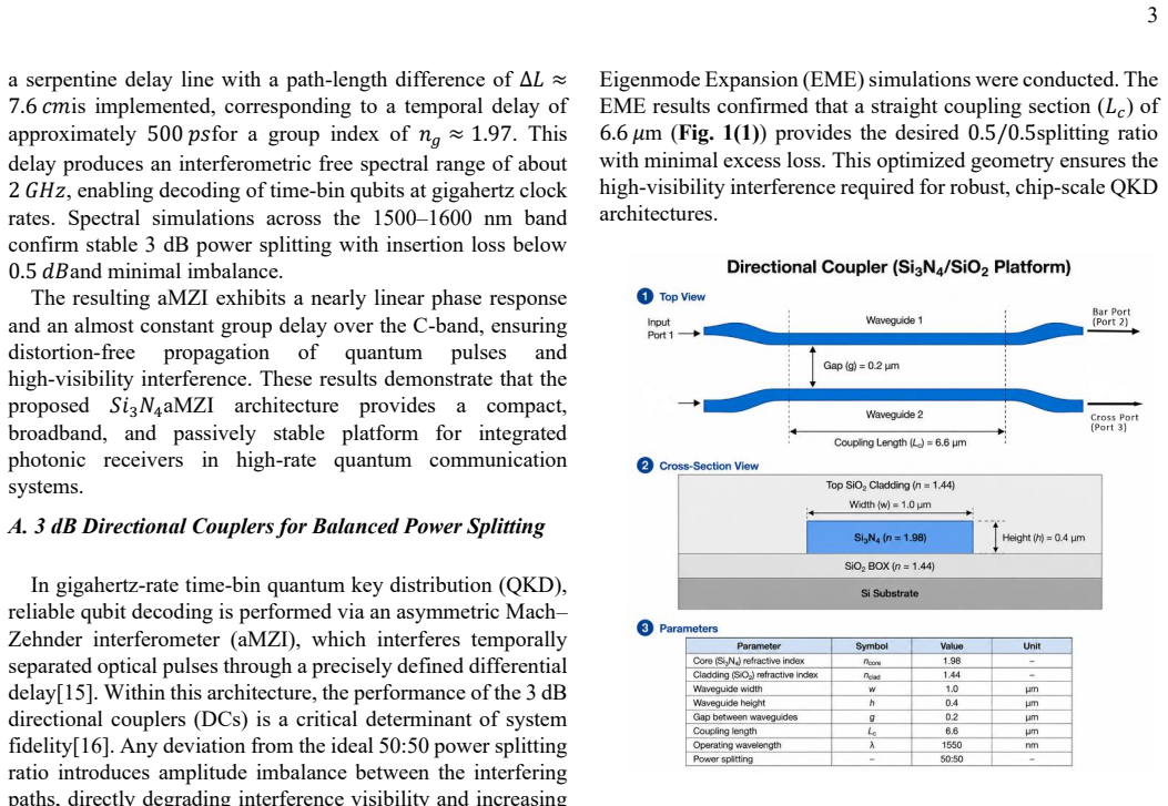
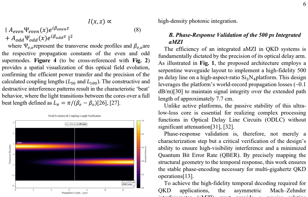
The 3 dB directional coupler whose coupling length is estimated from the effective index difference between even and odd supermodes and refined by three-dimensional eigenmode expansion simulations, paired with single-mode Si3N4 waveguides of 1 um x 0.4 um cross section.
If this is right
- The aMZI supports gigahertz-rate time-bin QKD with QBER below 0.5 percent.
- Wideband linear phase response allows compatibility with wavelength division multiplexed QKD systems.
- Insertion loss below 0.5 dB and stable splitting across the C-band enable low-loss integrated receivers.
- The 500 ps delay with sub-10 ps variation provides spectrally stable operation suitable for scalable chip-scale quantum photonic receivers.
Where Pith is reading between the lines
- The same waveguide platform could support multiple aMZIs on one chip for parallel QKD channels.
- The design approach may extend to other quantum protocols that require precise, stable timing references.
- Actual fabricated devices could be tested for tolerance to process variations by comparing measured visibility against the simulated 0.99 target.
Load-bearing premise
The 3D EME simulations and effective index calculations accurately capture the behavior of the actual fabricated device.
What would settle it
Fabricate the device and measure the actual interference visibility at 1550 nm; visibility below 0.99 would falsify the performance claim.
Figures
read the original abstract
Precise temporal delay generation is a key requirement for asymmetric Mach-Zehnder interferometers (aMZIs) used in high-speed quantum key distribution (QKD) receivers. In this work, a compact integrated aMZI architecture based on a silicon nitride on silicon dioxide (Si3N4/SiO2) photonic platform is presented. A 3-dB directional coupler enabling accurate 50:50 power splitting at the 1550 nm telecommunication wavelength is designed and optimized. The coupling length is initially estimated from the effective index difference between the even and odd supermodes and subsequently refined using three-dimensional eigenmode expansion (EME) simulations. The optimized structure employs single-mode Si3N4 waveguides with a cross section of 1 um x 0.4 um, providing a group index close to 2 and enabling accurate delay engineering. Spectral analysis demonstrates stable 3-dB power splitting across the C-band with insertion loss below 0.5 dB and negligible power imbalance, indicating high transmission efficiency and structural symmetry. An integrated Si3N4 aMZI delay line providing a 500 ps optical delay, corresponding to a 2 GHz free spectral range (FSR), is further demonstrated. Simulations show nearly constant group delay across the 190-200 THz frequency range with sub-10 ps variation and a smooth, near-linear phase response. These characteristics enable interference visibility above 0.99, corresponding to an estimated quantum bit error rate (QBER) below 0.5 percent for gigahertz-rate time-bin QKD systems. The wideband linear phase behavior also indicates compatibility with wavelength division multiplexed (WDM) QKD architectures. The results confirm that the proposed Si3N4 integrated aMZI provides a low-loss, dispersion-controlled, and spectrally stable delay solution suitable for scalable chip-scale quantum photonic receivers.
Editorial analysis
A structured set of objections, weighed in public.
Referee Report
Summary. The manuscript presents a simulated design for a compact Si3N4/SiO2 integrated asymmetric Mach-Zehnder interferometer (aMZI) using optimized 3 dB directional couplers for precise temporal delay generation in chip-scale QKD receivers. Based on effective-index calculations and 3D eigenmode expansion (EME) simulations of 1 µm × 0.4 µm single-mode waveguides, it reports a 500 ps delay line (2 GHz FSR) with stable 50:50 splitting (<0.5 dB insertion loss), sub-10 ps group-delay variation over 190–200 THz, near-linear phase response, interference visibility >0.99, and estimated QBER <0.5 %, concluding that the structure provides a low-loss, dispersion-controlled solution suitable for scalable quantum photonic receivers and WDM QKD.
Significance. If the simulated performance translates to fabricated devices, the design would address a practical need for compact, low-dispersion delay lines in gigahertz-rate time-bin QKD receivers on a standard low-loss photonic platform, with potential for WDM compatibility.
major comments (2)
- [Abstract / simulation results] Abstract and simulation results: The headline claims (visibility >0.99, QBER <0.5 %, suitability for scalable chip-scale receivers) rest entirely on idealized 3D EME simulations of group-delay flatness and coupler balance with no reported Monte-Carlo tolerance analysis or sensitivity study to fabrication variations in waveguide width, height, or etch depth. These variations directly affect the effective-index difference, coupling length, and resulting phase stability, making the mapping from simulation to device performance untested and load-bearing for the central claim.
- [Abstract] Abstract: No experimental validation, measured insertion loss, phase data, or comparison against fabricated reference devices is provided, so the assertion that the aMZI is “suitable for scalable chip-scale quantum photonic receivers” cannot be assessed beyond the idealized model.
Simulated Author's Rebuttal
We thank the referee for the constructive comments on our simulation-based design manuscript. We address each major comment below.
read point-by-point responses
-
Referee: [Abstract / simulation results] Abstract and simulation results: The headline claims (visibility >0.99, QBER <0.5 %, suitability for scalable chip-scale receivers) rest entirely on idealized 3D EME simulations of group-delay flatness and coupler balance with no reported Monte-Carlo tolerance analysis or sensitivity study to fabrication variations in waveguide width, height, or etch depth. These variations directly affect the effective-index difference, coupling length, and resulting phase stability, making the mapping from simulation to device performance untested and load-bearing for the central claim.
Authors: We agree that the absence of a Monte-Carlo tolerance or sensitivity analysis leaves the robustness against fabrication variations unquantified. In the revised manuscript we will add a sensitivity study that varies waveguide width (±10 nm), height (±5 nm), and etch depth around the nominal 1 µm × 0.4 µm cross-section and reports the resulting spreads in group-delay variation, coupler imbalance, and visibility. This will be presented alongside the idealized EME results to clarify the design margins. revision: yes
-
Referee: [Abstract] Abstract: No experimental validation, measured insertion loss, phase data, or comparison against fabricated reference devices is provided, so the assertion that the aMZI is “suitable for scalable chip-scale quantum photonic receivers” cannot be assessed beyond the idealized model.
Authors: The manuscript is explicitly a design and simulation study whose purpose is to propose and optimize the aMZI geometry using effective-index and 3D EME methods. Experimental fabrication, loss measurements, and phase characterization lie outside its scope; we have revised the abstract and conclusions to state that the simulated metrics indicate suitability for subsequent fabrication and testing rather than claiming demonstrated device performance. revision: no
- Experimental validation and measured data cannot be supplied because the work is a simulation-only design study.
Circularity Check
No circularity; performance metrics are direct outputs of standard EME and effective-index simulations
full rationale
The derivation chain begins with standard waveguide cross-section selection (1 µm × 0.4 µm) yielding group index ≈2, followed by effective-index estimation of coupling length that is then refined via independent 3D EME simulations. Spectral flatness, group-delay variation (<10 ps), and phase linearity are computed outputs of those simulations; visibility >0.99 and QBER <0.5 % are then inferred from the simulated phase stability using the conventional relation between visibility and error rate. No parameter is fitted to a target result, no self-citation supplies a uniqueness theorem or ansatz, and no quantity is redefined in terms of itself. The workflow is therefore self-contained against external simulation tools and does not reduce to its inputs by construction.
Axiom & Free-Parameter Ledger
free parameters (2)
- waveguide cross-section =
1 um x 0.4 um
- coupling length
axioms (2)
- domain assumption Effective index difference between even and odd supermodes determines the coupling length for 50:50 splitting
- domain assumption Group index remains close to 2 across the C-band for the chosen waveguide geometry
Reference graph
Works this paper leans on
-
[1]
Quantum cryptography
N. Gisin, G. Goire Ribordy, W. Tittel, and H. Zbinden, “Quantum cryptography.”
-
[2]
The security of practical quantum key distribution,
V. Scarani, H. Bechmann -Pasquinucci, N. J. Cerf, M. Dušek, N. Lütkenhaus, and M. Peev, “The security of practical quantum key distribution,” Rev. Mod. Phys. , vol. 81, no. 3, pp. 1301 –1350, Sep. 2009, doi: 10.1103/RevModPhys.81.1301
-
[3]
Secure quantum key distribution with realistic devices,
F. Xu, X. Ma, Q. Zhang, H. -K. Lo, and J. -W. Pan, “Secure quantum key distribution with realistic devices,” Rev. Mod. Phys. , vol. 92, no. 2, p. 025002, May 2020, doi: 10.1103/RevModPhys.92.025002
-
[4]
Distribution of Time -Bin Entangled Qubits over 50 km of Optical Fiber,
I. Marcikic, H. de Riedmatten, W. Tittel, H. Zbinden, M. Legré, and N. Gisin, “Distribution of Time -Bin Entangled Qubits over 50 km of Optical Fiber,” Phys. Rev. Lett., vol. 93, no. 18, p. 180502, Oct. 2004, doi: 10.1103/PhysRevLett.93.180502
-
[5]
M. Ren, L. Zhou, and Z. Yuan, “Low -loss, dual - polarization asymmetric Mach-Zehnder interferometer chips for quantum key distribution,” Science China Information Sciences, vol. 66, no. 8, p. 180503, Aug. 2023, doi: 10.1007/s11432-022-3641-x
-
[6]
Chip -based quantum key distribution,
P. Sibson et al. , “Chip -based quantum key distribution,” Nat. Commun. , vol. 8, Feb. 2017, doi: 10.1038/ncomms13984
-
[7]
Real-time operation of a multi-rate, multi-protocol quantum key distribution transmitter,
I. De Marco et al., “Real-time operation of a multi-rate, multi-protocol quantum key distribution transmitter,” Optica, vol. 8, no. 6, p. 911, Jun. 2021, doi: 10.1364/OPTICA.423517
-
[8]
Advances in Chip-Based Quantum Key Distribution,
Q. Liu et al., “Advances in Chip-Based Quantum Key Distribution,” Oct. 01, 2022, MDPI. doi: 10.3390/e24101334
-
[9]
Integrated photonic quantum technologies,
J. Wang, F. Sciarrino, A. Laing, and M. G. Thompson, “Integrated photonic quantum technologies,” Nat. Photonics, vol. 14, no. 5, pp. 273–284, May 2020, doi: 10.1038/s41566-019-0532-1
-
[10]
Real - time free spectral range measurement based on a correlated resonance -tracking technology,
C. Feng, X. Wang, B. Miao, Z. Gu, and J. Li, “Real - time free spectral range measurement based on a correlated resonance -tracking technology,” Opt. Express, vol. 31, no. 19, p. 30604, Sep. 2023, doi: 10.1364/OE.500573
-
[11]
Ultra-compact and robust mode division multiplexer based on a subwavelength grating structure,
Z. Liu, F. Xia, P. Wang, R. Yan, L. Chen, and M. Yuan, “Ultra-compact and robust mode division multiplexer based on a subwavelength grating structure,” Optics Continuum, vol. 5, no. 3, p. 840, Mar. 2026, doi: 10.1364/OPTCON.589039
-
[12]
K. Yoshino, T. Ochi, M. Fujiwara, M. Sasaki, and A. Tajima, “Maintenance -free operation of WDM quantum key distribution system through a field fiber 15 over 30 days,” Opt. Express, vol. 21, no. 25, p. 31395, Dec. 2013, doi: 10.1364/OE.21.031395
-
[13]
Integrated silicon photonics for high -speed quantum key distribution,
P. Sibson, J. E. Kennard, S. Stanisic, C. Erven, J. L. O’Brien, and M. G. Thompson, “Integrated silicon photonics for high -speed quantum key distribution,” Optica, vol. 4, no. 2, p. 172, Feb. 2017, doi: 10.1364/optica.4.000172
-
[14]
Elsevier,
Theory of Dielectric Optical Waveguides . Elsevier,
-
[15]
doi: 10.1016/B978-0-12-470951-5.X5001-X
-
[17]
Asymmetric, non -uniform 3 -dB directional coupler with 300-nm bandwidth and a small footprint,
H. Nikbakht et al. , “Asymmetric, non -uniform 3 -dB directional coupler with 300-nm bandwidth and a small footprint,” Opt. Lett., vol. 48, no. 2, p. 207, Jan. 2023, doi: 10.1364/OL.476537
-
[18]
Design of a large bandwidth 2 × 2 interferometric switching cell based on a sub-wavelength grating,
G. Brunetti, G. Marocco, A. Di Benedetto, A. Giorgio, M. N. Armenise, and C. Ciminelli, “Design of a large bandwidth 2 × 2 interferometric switching cell based on a sub-wavelength grating,” Journal of Optics, vol. 23, no. 8, p. 085801, Sep. 2021, doi: 10.1088/2040 - 8986/ac0a8c
-
[20]
Development of high quality silicon nitride chips for integrated nonlinear photonics,
Houssein el Dirani, “Development of high quality silicon nitride chips for integrated nonlinear photonics,” Université de Lyon, 2019
2019
-
[21]
A photonic integrated quantum secure communication system,
T. K. Paraïso et al. , “A photonic integrated quantum secure communication system,” Nat. Photonics , vol. 15, no. 11, pp. 850 –856, Nov. 2021, doi: 10.1038/s41566-021-00873-0
-
[22]
H. A. . Haus, Waves and fields in optoelectronics . Prentice-Hall, 1984
1984
-
[23]
Silicon nitride Mach -Zehnder interferometer for on -chip quantum random number generation,
A. Prokhodtsov et al., “Silicon nitride Mach -Zehnder interferometer for on -chip quantum random number generation,” J. Phys. Conf. Ser. , vol. 1695, no. 1, p. 012118, Dec. 2020, doi: 10.1088/1742 - 6596/1695/1/012118
-
[24]
New CMOS -compatible platforms based on silicon nitride and Hydex for nonlinear optics,
D. J. Moss, R. Morandotti, A. L. Gaeta, and M. Lipson, “New CMOS -compatible platforms based on silicon nitride and Hydex for nonlinear optics,” Nat. Photonics, vol. 7, no. 8, pp. 597 –607, Aug. 2013, doi: 10.1038/nphoton.2013.183
-
[25]
R. S. El Shamy, A. E. Afifi, M. M. Badr, and M. A. Swillam, “Modelling, characterization, and applications of silicon on insulator loop terminated asymmetric Mach Zehnder interferometer,” Sci. Rep., vol. 12, no. 1, p. 3598, Mar. 2022, doi: 10.1038/s41598- 022-07449-0
-
[26]
L. Chrostowski and M. Hochberg, Silicon Photonics Design. Cambridge University Press, 2015. doi: 10.1017/CBO9781316084168
-
[27]
Universal relations for coupling of optical powerbetweenmicroresonators and dielectric waveguides,
A. Yariv, “Universal relations for coupling of optical powerbetweenmicroresonators and dielectric waveguides,” Electron. Lett., vol. 36, no. 4, pp. 321 – 322, Feb. 2000, doi: 10.1049/el:20000340
-
[28]
Theory of Dielectric Waveguides,
H. Kogelnik, “Theory of Dielectric Waveguides,” 1975, pp. 13–81. doi: 10.1007/978-3-662-43208-2_2
-
[29]
A. W. Snyder and J. D. Love, Optical Waveguide Theory. Boston, MA: Springer US, 1984. doi: 10.1007/978-1-4613-2813-1
-
[30]
Silicon Nitride in Silicon Photonics,
D. J. Blumenthal, R. Heideman, D. Geuzebroek, A. Leinse, and C. Roeloffzen, “Silicon Nitride in Silicon Photonics,” Dec. 01, 2018, Institute of Electrical and Electronics Engineers Inc. doi: 10.1109/JPROC.2018.2861576
-
[31]
Silicon nitride passive and active photonic integrated circuits: trends and prospects,
C. Xiang, W. Jin, and J. E. Bowers, “Silicon nitride passive and active photonic integrated circuits: trends and prospects,” Photonics Res., vol. 10, no. 6, p. A82, Jun. 2022, doi: 10.1364/PRJ.452936
-
[32]
Ultra -low loss optical delay lines based on silicon nitride SWG technology,
M. Tosi, M. C. Bustillos, H. Sun, L. A. Bulus -Rossini, J. Azaña, and P. A. Costanzo -Caso, “Ultra -low loss optical delay lines based on silicon nitride SWG technology,” Opt. Express, vol. 33, no. 16, p. 33351, Aug. 2025, doi: 10.1364/OE.561965
-
[33]
Ultra-low-loss optical delay line on a silicon chip,
H. Lee, T. Chen, J. Li, O. Painter, and K. J. Vahala, “Ultra-low-loss optical delay line on a silicon chip,” Nat. Commun., vol. 3, no. 1, p. 867, May 2012, doi: 10.1038/ncomms1876
-
[34]
Metropolitan Quantum Key Distribution with Silicon Photonics,
D. Bunandar et al. , “Metropolitan Quantum Key Distribution with Silicon Photonics,” Phys. Rev. X, vol. 8, no. 2, p. 021009, Apr. 2018, doi: 10.1103/PhysRevX.8.021009
-
[35]
TriPleX: a versatile dielectric photonic platform,
K. Wörhoff, R. G. Heideman, A. Leinse, and M. Hoekman, “TriPleX: a versatile dielectric photonic platform,” Advanced Optical Technologies, vol. 4, no. 2, pp. 189 –207, Apr. 2015, doi: 10.1515/aot -2015- 0016
work page doi:10.1515/aot 2015
-
[36]
Integrated Optical Tunable Delay Line and Microwave Photonic Beamforming Chip: A Review,
S. Shi et al., “Integrated Optical Tunable Delay Line and Microwave Photonic Beamforming Chip: A Review,” Laser Photon. Rev., vol. 19, no. 7, Apr. 2025, doi: 10.1002/lpor.202400663
-
[37]
Stable quantum key distribution using a silicon photonic transceiver,
W. Geng, C. Zhang, Y. Zheng, J. He, C. Zhou, and Y. Kong, “Stable quantum key distribution using a silicon photonic transceiver,” Opt. Express, vol. 27, no. 20, p. 29045, Sep. 2019, doi: 10.1364/OE.27.029045
-
[38]
I. Essadeq, S. Nafiri, S. Benjelloun, and A. E. Fettouh, “Stability and convergence of modal approximations in coupled thermoelastic systems: Theory and simulation,” Discrete and Continuous Dynamical Systems - S, vol. 0, no. 0, pp. 0 –0, 2026, doi: 10.3934/dcdss.2026070
-
[39]
G. F. R. Chen, J. R. Ong, T. Y. L. Ang, S. T. Lim, C. E. Png, and D. T. H. Tan, “Broadband Silicon -On- Insulator directional couplers using a combination of straight and curved waveguide sections,” Sci. Rep., vol. 7, no. 1, p. 7246, Aug. 2017, doi: 10.1038/s41598-017- 07618-6
-
[40]
Broadband Directional Coupler Based on Deformed Circular Waveguide for High -Power Application,
M. Wang, X. Liao, P. Liu, Z. Li, and W. Li, “Broadband Directional Coupler Based on Deformed Circular Waveguide for High -Power Application,” Electronics (Basel)., vol. 14, no. 13, p. 2652, Jun. 2025, doi: 10.3390/electronics14132652
-
[41]
Broadband integrated directional 16 coupler for heralded single -photon characterization,
F. Castro -Simanca, F. A. Domínguez -Serna, M. Gómez-Robles, R. Salas-Montiel, W. De La Cruz, and K. Garay -Palmett, “Broadband integrated directional 16 coupler for heralded single -photon characterization,” Journal of the Optical Society of America B , vol. 42, no. 11, p. B58, Nov. 2025, doi: 10.1364/JOSAB.572117
-
[42]
Supermode -based second harmonic generation in a nonlinear interferometer,
D. Barral et al. , “Supermode -based second harmonic generation in a nonlinear interferometer,” Opt. Express, vol. 29, no. 23, p. 37175, Nov. 2021, doi: 10.1364/OE.435281
-
[43]
Advances in Chip -Scale Quantum Photonic Technologies,
L. Lu, X. Zheng, Y. Lu, S. Zhu, and X. S. Ma, “Advances in Chip -Scale Quantum Photonic Technologies,” Dec. 01, 2021, John Wiley and Sons Inc. doi: 10.1002/qute.202100068
discussion (0)
Sign in with ORCID, Apple, or X to comment. Anyone can read and Pith papers without signing in.