REVIEW 4 major objections 6 minor 2 references
Improving Performance of Tin-Doped-Zinc-Oxide Thin-Film Transistors by Optimized Multi-Stacked Active-Layer Structures
T0 review · 4 major / 6 minor · reviewed 2026-08-14 · deepseek-v4-flash
Pith's one-line read Sandwiching a conductive ITO film between two TZO layers gives oxide transistors both low leakage and high mobility.
desk verdict Useful incremental device work with a new TZO/ITO/TZO stack, but the headline comparison rests on single-device curves without error bars; deserves peer review with mandatory statistics. read the letter →
The pith
A machine-rendered reading of the paper's core claim, the machinery that carries it, and where it could break.
The reading
What carries the argument
The load-bearing object is the triple-active-layer stack TZO/ITO/TZO (22 nm / 5 nm / 22 nm), with the high-carrier-density ITO film supplying on-state charge and the two lower-carrier-density TZO cladding layers controlling off-state leakage. The accompanying simplified resistance model splits the total channel resistance into electrode and contact resistances plus the resistances of each sub-layer, and it is this model that explains why the TAL stack's total resistance sits between the SAL and DAL values—high enough to keep $I_{off}$ at 3.3 pA, low enough to preserve a saturation mobility above $100\ \mathrm{cm^2/V\,s}$ at all tested channel lengths.
What would settle it
Fabricate SAL, DAL, and TAL devices in interleaved batches on the same substrate run, measure several devices per split, and check whether the TAL stack reproducibly gives an on-off ratio near $2\times10^8$ with an off-current near $3.3\ \mathrm{pA}$; if the TAL off-current falls within batch scatter of the DAL values, or if varying the TZO cladding thickness does not raise channel resistance as the series-resistance model predicts, the central claim would be refuted.
Extended reading notes
Core claim
The paper's central claim is that replacing a dual ITO/TZO channel by a triple TZO/ITO/TZO stack suppresses the dual layer's main weakness—its high off-state current—while keeping its advantages. The authors report that the triple-layer devices show roughly the same channel resistivity as a single TZO layer (about 20 times larger than the DAL stack), which their simplified series-resistance model attributes to the outer TZO layers adding series resistance, while the central ITO layer still provides enough carrier density for high on-current and mobility. The measured figures for the TAL devices are an on-off ratio of $2\times10^8$, $\mu_{sat}=145.2\ \mathrm{cm^2/V\,s}$, $V_{th}=0.52\ \mathrm{V}$, and $I_{off}=3.3\ \mathrm{pA}$, and the authors take the consistent performance of TAL TFTs at channel lengths 20–100 µm as evidence of process stability.
Load-bearing premise
The load-bearing premise is that the single-layer and dual-layer devices are fair, representative baselines, with the channel stack as the only meaningful variable; the paper states their SAL and DAL thicknesses were optimized but gives no device counts or error bars, so if batch-to-batch variation instead drives the differences, the TAL advantage would not be established.
Editorial extensions
If this is right
- If the triple-layer result holds, display backplanes can be made entirely below 80 °C by sputtering, so heat-sensitive polymer substrates become viable without high-temperature annealing.
- The measured on-off ratio of $2\times10^8$ with an off-current of $3.3\ \mathrm{pA}$ means a TAL pixel switch leaks little charge in the off state, reducing holding-voltage droop and power consumption in active-matrix displays.
- Saturation mobility above $100\ \mathrm{cm^2/V\,s}$ at channel lengths 20, 80, and 100 µm indicates the process could support different pixel layouts without changing the channel material.
- The resistance model gives a design rule: the TZO cladding thickness can be tuned to trade off-current against on-current, so similar stacks could be optimized for other oxide semiconductors.
Reading between the lines
- A natural extension the paper does not test is whether the same conductive-core/resistive-cladding sandwich works with other high-mobility cores, such as IGZO or IZO, and other wide-gap claddings, which would make the design a general oxide-channel architecture.
- Because the reported comparison uses one representative device per configuration and no error bars, the strongest direct test is a batch study; if inter-batch variation is comparable to the reported differences, the mechanism would need re-examination.
- The paper states the TAL stack itself has not been thickness-optimized, so the reported $145.2\ \mathrm{cm^2/V\,s}$ and $3.3\ \mathrm{pA}$ are plausibly not the endpoint; systematic variation of the TZO cladding thickness could improve both, subject to the series-resistance trade-off.
- The resistance model implies a limit: if the TZO cladding becomes too thick, on-state mobility will drop because the conductive ITO core is shunted by series resistance, so optimization is a balance rather than a monotonic improvement.
Signed reviews
Editorial analysis
A structured set of objections, weighed in public.
Referee Report
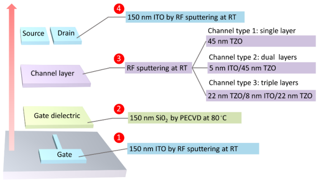
Summary. The paper reports the fabrication and electrical characterization of tin-doped zinc oxide (TZO) thin-film transistors with three channel configurations: single active layer (SAL, 45 nm TZO), dual active layer (DAL, 5 nm ITO / 45 nm TZO), and triple active layer (TAL, 22 nm TZO / 5 nm ITO / 22 nm TZO), all processed at temperatures below 80°C on glass. The central claim is that TAL TFTs combine the low off-state current of SAL TFTs with the high saturation mobility and low threshold voltage of DAL TFTs, achieving an on-off current ratio of approximately 2×10^8, a threshold voltage of 0.52 V, a saturation mobility of 145.2 cm²/Vs, and an off-state current of 3.3 pA. The authors support this claim with representative transfer and output curves, extracted parameters summarized in Table 1, a qualitative resistance model, and material characterization (AFM, SEM, XRD). They also present TAL TFTs at three channel lengths to argue for process uniformity.
Significance. If the reported performance and the comparison across channel configurations are reliable, the work demonstrates a low-temperature, simple-process oxide TFT channel design that is potentially attractive for flexible display backplanes. The qualitative physics—that a thin ITO layer raises on-state mobility while surrounding TZO layers suppress off-state leakage—is plausible and internally consistent with the shown transfer curves. The paper also provides useful material characterization and a transparent statement that the TAL stack is not yet fully optimized. However, the quantitative headline parameters and the comparative claims currently rest on single-device measurements, a common-capacitance mobility extraction, and an unsubstantiated assertion that channel-thickness effects have been eliminated. These issues must be addressed before the central claim can be considered established.
major comments (4)
- [Results, Fig. 3d and Table 1] The central claim that TAL TFTs combine the advantages of SAL and DAL TFTs rests on a comparison of single representative transfer curves and single extracted parameter values. No device counts, error bars, or batch-to-batch controls are reported anywhere in the manuscript. As a result, the reported values of Ion/Ioff = 2×10^8, Ioff = 3.3 pA, and μsat = 145.2 cm²/Vs cannot be distinguished from device-to-device or run-to-run variation. Please provide statistics (at least 3–5 devices per configuration) and explain how the representative devices were selected.
- [Results, Eq. (3) and Cox statement] The saturation mobility is extracted from Eq. (3) using a single Cox value (quoted as 2.6×10^8 F/cm², presumably a typo for 2.6×10^−8 F/cm²) for all three channel stacks. The stacks differ in total semiconductor thickness and layer sequence (45 nm TZO; 5 nm ITO/45 nm TZO; 22 nm TZO/5 nm ITO/22 nm TZO), so the effective gate-to-channel capacitance is not necessarily the same for each configuration. Using one Cox for all devices biases the extracted mobilities and makes the headline value of 145.2 cm²/Vs uncertain. Please measure or calculate Cox separately for each stack, or provide a sensitivity analysis quantifying the effect of the capacitance assumption.
- [Discussion] The statement that "the thickness of the channel layers of the SAL TFTs and DAL TFTs in this research has been optimized. Thus, we can eliminate the effect of channel thickness" is not supported by the data presented. The three configurations differ not only in total thickness (45, 50, and 49 nm) but also in the position of the ITO layer relative to the gate and to the top surface, so "stack configuration" is not the only independent variable. Furthermore, the paper states that the TAL stack is not yet optimized while the SAL and DAL thicknesses are described as optimized, which leaves open the possibility that a different TAL thickness or a differently optimized DAL stack could change the ranking. A thickness-matched comparison set, or an explicit treatment of layer geometry and total thickness, would be needed to support the claim that the TAL configuration itself, rather than incidental thickness differences, is responsible for the observed performance.
- [Results, Fig. 6b and Table 1] The conclusion that the fabrication process is "stable and uniform" is based on representative transfer curves at three channel lengths (20, 80, and 100 µm), with no indication of how many devices per length were measured. Similar transfer curves at different channel lengths demonstrate expected scaling behavior but do not establish uniformity across a process. Please provide multiple devices per channel length and report means and standard deviations for the extracted parameters.
minor comments (6)
- [Abstract/Introduction] There are several typographical errors: "comb ine" in the abstract, "2-dimentional" in the Introduction, and "reduction the hole density" in the Discussion (the channel is n-type, so this should read "electron density" or "carrier density").
- [Methods] The gas mixture is written as "N20" and should be "N2O"; the Cox value is written as "2.6×10^8 F/cm2" and should presumably be "2.6×10^−8 F/cm2".
- [Results, Eq. (4)] The layout around Eq. (4) is confusing: the text reads "Using the equation (4):" followed by a blank line before the equation is displayed. Please place the equation immediately after its introduction.
- [Results, Fig. 7 caption] The scale bar in the Fig. 7 caption is given as "200 µm"; for AFM images of thin films this is almost certainly a typo for "200 nm". Please correct the unit.
- [Results, XRD discussion] The designation of the TZO film as "C-axis-aligned crystalline (CAAC)" is based on a single XRD peak at 34.3° and the Scherrer grain size. This is suggestive but not conclusive; additional evidence such as cross-sectional TEM or pole-figure analysis would strengthen the claim.
- [Methods, channel resistivity] The phrase "The channel resistivity was obtained from four-probe station" is ambiguous: clarify whether this is a four-point probe measurement on the deposited films or on the device channel, and specify the measurement conditions (e.g., gate bias).
Circularity Check
No significant circularity: the central TAL-performance claim is a direct experimental comparison, and the resistance model is a post hoc description using Ohm's law rather than a fitted prediction.
full rationale
No load-bearing derivation chain reduces to its own inputs. The paper's central claim, that TZO/ITO/TZO triple-active-layer TFTs combine the low off-current of SAL TFTs with the high mobility and low threshold voltage of DAL TFTs, is an empirical comparison of measured transfer curves (Fig. 3d) and extracted parameters (Table 1), not a prediction from a fitted model. The 'simplified resistance model' is qualitative: Ioff = VDS/Roverall (Eq. 4) is Ohm's law, and the channel resistivity in Fig. 4d is measured by a four-probe station, so using it to rationalize the observed lower off-current is a post hoc physical explanation rather than a self-definitional prediction. The paper relies on its own prior reports (refs 27-31) for context and for the assertion that SAL and DAL channel thicknesses were optimized; these citations support the experimental baseline but do not define or force the measured TAL parameters, so they are not load-bearing in the circularity sense. Weaknesses such as single representative devices, lack of error bars or device counts, and the explicitly unoptimized TAL stack are statistical and validity concerns (correctness risk), not circularity. The comparison across channel configurations is not a derivation from inputs, and no uniqueness theorem or ansatz is imported.
Assumptions & free parameters
assumptions (4)
- standard math Off-state current is governed by total resistance through Ohm's law (Ioff = VDS/Roverall).
- domain assumption The active stack can be represented as series resistances of individual TZO and ITO layers with no parallel leakage path through the ITO layer.
- domain assumption SAL and DAL channel thicknesses are optimized so that thickness effects can be ignored when comparing configurations.
- domain assumption The Cox value (2.6×10^-8 F/cm2) measured from a 100-kHz C-V curve is valid for all three device types in saturation mobility extraction.
Cite this review
Pith. "Pith review of Improving Performance of Tin-Doped-Zinc-Oxide Thin-Film Transistors by Optimized Multi-Stacked Active-Layer Structures." pith.science (2026). https://pith.science/paper/QRFPH476
@misc{pith2026190809829,
  author       = {Pith},
  title        = {Pith review of: Improving Performance of Tin-Doped-Zinc-Oxide Thin-Film Transistors by Optimized Multi-Stacked Active-Layer Structures},
  year         = {2026},
  howpublished = {\url{https://pith.science/paper/QRFPH476}},
  note         = {Machine review of arXiv:1908.09829}
}
read the original abstract
In this paper, we investigated the performance of thin-film transistors (TFTs) with different channel configurations including single-active-layer (SAL) Sn-Zn-O (TZO), dual-active-layers (DAL) In-Sn-O (ITO)/TZO, and triple-active-layers (TAL) TZO/ITO/TZO. The TAL TFTs were found to combine the advantages of SAL TFTs (a low off-state current) and DAL TFTs (a high mobility and a low threshold voltage). The proposed TAL TFTs exhibit superior electrical performance, e.g. a high on-off state current ratio of 2*10^8, a low threshold voltage of 0.52 V, a high saturation mobility of 145.2 cm2/Vs, and a low off-state current of 3.3 pA. The surface morphology and characteristics of the ITO and TZO films were investigated and the TZO film was found to be C-axis-aligned crystalline (CAAC). A simplified resistance model was deduced to explain the high channel resistance of TAL TFTs. At last, TAL TFTs with different channel lengths were also discussed to show the stability and the uniformity of our fabrication process. Owing to its low-processing temperature, superior electrical performance, and low cost, TFTs with the proposed TAL channel configuration are highly promising for flexible displays where the use of heat-sensitive polymeric substrates is desirable.
Figures


Reference graph
Works this paper leans on
-
[1]
1 Kwon, J. Y. & Jeong, J. K. Recent progress in high performance and reliable n-type transition metal oxide-based thin film transistors. Semicond Sci Tech 30 (2015). 2 Hoffman, R. L., Norris, B. J. & Wager, J. F. ZnO -based transparent thin-film transistors. Appl Phys Lett 82, 733-735 (2003). 3 Nomura, K. et al. Room-temperature fabrication of transparent...
work page 2015
-
[2]
Cong, Lingling Huang, Yi Zhang, Shengdong Zhang, Xing Zhang, Yi Wang. P ‐16: The Research of Dual‐Layer Channel ITO/MZO Thin Film Transistors Fabricated on Glass at Low Temperature. SID Symposium Digest of Technical Papers 46, 1176-1179 (2015). 12 Jing Wu, D. H., Nannan Zhao, Zhuofa Chen, Yingying Cong, Feilong Zhao, Junchen Dong, Shengdong Zhang, Xing Zh...
Reviewed August 14, 2026 · model on record in the stance chip above.
Discussion (0). Continue with ORCID to comment.