Surface Modification for III-V Selective Area Molecular Beam Epitaxy of Non-Selective Mask Materials
Pith reviewed 2026-06-28 13:34 UTC · model grok-4.3
The pith
A sub-1 nm SiO2 cap layer imparts SiO2-like selectivity to any mask material for III-V selective-area MBE while preserving its infrared optical response.
A machine-rendered reading of the paper's core claim, the machinery that carries it, and where it could break.
Core claim
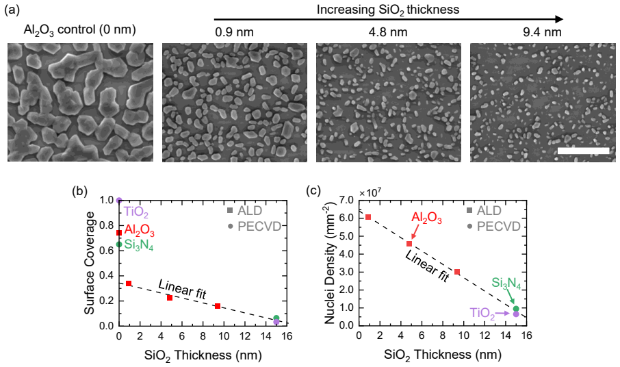
The paper establishes that a thin SiO2 capping layer applied to non-selective mask films such as Si3N4 and TiO2 enables selective-area embedded regrowth of III-V semiconductors by molecular beam epitaxy under growth conditions typical of the GaAs/SiO2 system, with the relationship between cap thickness and selectivity showing that sub-1 nm layers are effective at altering surface chemistry while leaving the mask's optical response intact.
What carries the argument
The sub-1 nm SiO2 capping layer that modifies mask surface chemistry to enforce selective growth.
If this is right
- Al2O3 exhibits selective growth within typical GaAs temperature ranges.
- HfO2 remains dominated by Ga adsorption and non-selective up to 650 °C.
- TiO2 and Si3N4, previously unusable, become selective with the cap.
- The cap thickness-selectivity curve indicates that layers below 1 nm are already effective.
- The method allows integration of metals and dielectrics into crystalline III-V material using masks chosen for optical performance rather than growth compatibility.
Where Pith is reading between the lines
- Device designers could now select mask materials primarily for refractive index contrast in mid-infrared photonics rather than growth compatibility.
- The same capping process might be tested on other epitaxial techniques or substrate orientations to broaden its utility.
- Interface studies between the cap and the III-V regrowth layer could reveal whether the thin oxide affects carrier transport or defect density at the mask edge.
- Scaling the approach to larger wafers would require verifying uniformity of the sub-nanometer cap deposition.
Load-bearing premise
The ultrathin SiO2 cap adds no significant optical absorption, scattering, or interface defects that would cancel the spectral gains of the base mask material.
What would settle it
Spectroscopic measurement of a capped versus uncapped mask film showing a measurable increase in extinction coefficient or drop in transmission at the target infrared wavelengths.
Figures
read the original abstract
Selective-area embedded regrowth of III-V semiconductors by molecular beam epitaxy enables the seamless integration of metals and dielectrics into crystalline material for novel design of optoelectronic devices. However, traditional masks like $SiO_2$ and $Si_{3}N_{4}$ limit the design of high-contrast photonics in the infrared due to their high extinction coefficients at technologically relevant wavelengths. Consequently, there is a need to explore alternative mask materials to expand the selective area molecular beam epitaxy capabilities beyond those traditionally used. This study evaluates the deposition selectivity of the alternative materials $Al_{2}O_{3}$, $TiO_2$, and $HfO_2$, films with preferable spectral responses but higher surface reactivity. It was found that $Al_{2}O_{3}$ exhibits promising selective growth characteristics within typical GaAs growth temperatures, $HfO_2$ demonstrated a high non-selectivity dominated by Ga adsorption on the mask at temperatures up to 650 $^\circ$C, and $TiO_2$ proved reactive during deposition. To achieve selective growth of highly non-selective and even reactive mask materials, a surface modification technique was employed to improve the selective growth characteristics of any given film. Selective growth of $Si_{3}N_{4}$ and $TiO_2$ films was achieved with the application of a thin $SiO_2$ capping layer utilizing growth conditions typical of the GaAs/$SiO_2$ system. The relationship between the thickness of $SiO_2$ caps and growth selectivity was examined, revealing that sub-1 nm capping layers can significantly influence the mask surface chemistry, indicating that by depositing a thin layer of $SiO_2$, $SiO_2$-like selectivity for any mask material can be realized without degrading its optical response.
Editorial analysis
A structured set of objections, weighed in public.
Referee Report
Summary. The manuscript reports MBE growth experiments showing that Al2O3 exhibits promising selectivity for GaAs at typical temperatures, while HfO2 shows high non-selectivity due to Ga adsorption up to 650°C and TiO2 is reactive during deposition. It further demonstrates that a sub-1 nm SiO2 capping layer imparts SiO2-like selectivity to otherwise non-selective or reactive masks such as Si3N4 and TiO2, and claims this modification realizes the desired selectivity without degrading the superior IR optical response of the underlying material.
Significance. If the optical-preservation claim holds, the surface-modification technique would meaningfully expand the set of usable mask materials for selective-area III-V regrowth, enabling higher-contrast infrared photonics without sacrificing growth selectivity. The experimental demonstration of selectivity control via sub-nm caps is a concrete, potentially transferable result.
major comments (2)
- [Abstract] Abstract: the central claim that 'sub-1 nm capping layers ... [realize] SiO2-like selectivity for any mask material ... without degrading its optical response' is load-bearing yet unsupported by data. No ellipsometry, FTIR, transmission, or scattering measurements are reported for capped versus uncapped Al2O3, TiO2, or HfO2 films at the wavelengths where these materials are claimed to outperform SiO2.
- [Abstract] The selectivity results are presented only qualitatively ('promising,' 'high non-selectivity,' 'achieved'). No growth-rate ratios, SEM/AFM coverage statistics, or temperature-dependent selectivity windows with error bars are provided, making it impossible to assess how close the capped films come to true SiO2 performance or how robust the result is.
minor comments (2)
- Growth-condition details (V/III ratio, As overpressure, exact substrate temperature calibration) are referenced only as 'typical of the GaAs/SiO2 system' without numerical values, hindering reproducibility.
- The manuscript should clarify whether the SiO2 cap thickness was measured by ellipsometry or TEM and whether any interface roughness or pinhole density was characterized after capping.
Simulated Author's Rebuttal
We thank the referee for their thoughtful review and constructive criticism. We respond to each major comment below, indicating where revisions will be made to strengthen the manuscript.
read point-by-point responses
-
Referee: [Abstract] Abstract: the central claim that 'sub-1 nm capping layers ... [realize] SiO2-like selectivity for any mask material ... without degrading its optical response' is load-bearing yet unsupported by data. No ellipsometry, FTIR, transmission, or scattering measurements are reported for capped versus uncapped Al2O3, TiO2, or HfO2 films at the wavelengths where these materials are claimed to outperform SiO2.
Authors: We agree that the manuscript contains no direct optical measurements (ellipsometry, FTIR, etc.) comparing capped and uncapped films. The statement in the abstract is an inference drawn from the sub-1 nm cap thickness being a negligible fraction of the underlying film. To correct this, we will revise the abstract to remove the unsubstantiated claim about optical response preservation and instead state only what was experimentally demonstrated (selectivity improvement). A brief discussion of the expected optical impact based on thickness can be added if the editor permits, but we will not assert preservation without data. revision: yes
-
Referee: [Abstract] The selectivity results are presented only qualitatively ('promising,' 'high non-selectivity,' 'achieved'). No growth-rate ratios, SEM/AFM coverage statistics, or temperature-dependent selectivity windows with error bars are provided, making it impossible to assess how close the capped films come to true SiO2 performance or how robust the result is.
Authors: The abstract and main text do present selectivity outcomes qualitatively. While the full manuscript includes SEM images showing growth outcomes on the various masks, we acknowledge the absence of extracted quantitative metrics such as growth-rate ratios or statistical coverage data with uncertainties. We will revise the manuscript to include quantitative analysis of the existing SEM data (e.g., estimated growth rates and coverage fractions) and will add a short discussion of the temperature range explored. Full error-bar analysis would require additional measurements not performed in this study. revision: partial
Circularity Check
No circularity: purely experimental reporting with no derivations or fitted predictions
full rationale
The manuscript consists entirely of experimental observations on mask material selectivity during MBE growth, including tests of Al2O3, HfO2, TiO2, and the effect of sub-1 nm SiO2 caps on Si3N4 and TiO2. No equations, parameters, models, or derivations appear in the provided text or abstract. The central claim that thin SiO2 confers SiO2-like selectivity 'without degrading its optical response' is presented as an inference from growth experiments rather than from any self-referential calculation or self-citation chain. Because there is no derivation chain to inspect, none of the enumerated circularity patterns (self-definitional, fitted-input-as-prediction, etc.) can apply. The paper is self-contained against external benchmarks as a report of observed phenomena.
Axiom & Free-Parameter Ledger
axioms (2)
- domain assumption Typical GaAs MBE growth temperatures (around 500-650 C) and fluxes produce the reported selectivity behaviors on SiO2.
- domain assumption Al2O3, TiO2, and HfO2 films possess lower extinction coefficients than SiO2 or Si3N4 in the infrared.
Reference graph
Works this paper leans on
-
[1]
Viard, Jocelyn and Bêche, E. and Perarnau, D. and Berjoan, R. and Durand, J. , year =. doi:10.1016/S0955-2219(97)00051-4 , journal =
-
[2]
Journal of Materials Science , author =
Influence of process conditions on the surface oxidation of silicon nitride green compacts , doi =. Journal of Materials Science , author =
-
[3]
New Journal of Physics , abstract =
Heindel, Tobias and Kessler, Christian A and Rau, Markus and Schneider, Christian and Fürst, Martin and Hargart, Fabian and Schulz, Wolfgang-Michael and Eichfelder, Marcus and Roßbach, Robert and Nauerth, Sebastian and Lermer, Matthias and Weier, Henning and Jetter, Michael and Kamp, Martin and Reitzenstein, Stephan and Höfling, Sven and Michler, Peter...
-
[4]
R.S. Dubey and V. Ganesan , keywords =. Fabrication and characterization of TiO2/SiO2 based Bragg reflectors for light trapping applications , journal =. 2017 , issn =. doi:https://doi.org/10.1016/j.rinp.2017.06.041 , url =
-
[5]
Selective area epitaxy of PbTe-Pb hybrid nanowires on a lattice-matched substrate , author =. Phys. Rev. Mater. , volume =. 2022 , month =. doi:10.1103/PhysRevMaterials.6.034205 , url =
-
[6]
Area selective epitaxy of GaAs with AlGaAs native oxide mask by molecular beam epitaxy , doi =
Yoshiba, Ippei and Iwai, Takayuki and Uehara, Takahiro and Horíkoshi, Yoshiji , journal =. Area selective epitaxy of GaAs with AlGaAs native oxide mask by molecular beam epitaxy , doi =. 2007 , researchRabbitId =
2007
-
[7]
Mechanism of Selective Area Growth by MBE , doi =
Kishino, Katsumi , journal =. Mechanism of Selective Area Growth by MBE , doi =. 2019 , researchRabbitId =
2019
-
[8]
and Benedicto, Marcos , journal =
Tejedor, P. and Benedicto, Marcos , journal =. Selective area growth of InxGa1-xAs nanowires on HfO2 templates for highly scaled nMOS devices , doi =. 2019 , researchRabbitId =
2019
-
[9]
Deposition of thin indium oxide film and its application to selective epitaxy for in situ processing , doi =
Ozasa, Kazunari and Ye, Tianchun and Aoyagi, Yoshinobu , journal =. Deposition of thin indium oxide film and its application to selective epitaxy for in situ processing , doi =. 1994 , researchRabbitId =
1994
-
[10]
Effect of mask material on selective growth of GaN by RF-MBE , doi =
Nagae, Yuki and Iwatsuki, Takenori and Shirai, Yuya and Osawa, Yuki and Naritsuka, Shigeya and Maruyama, Takahiro , journal =. Effect of mask material on selective growth of GaN by RF-MBE , doi =. 2011 , researchRabbitId =
2011
-
[11]
Improved Ti-mask selective-area growth (SAG) by rf-plasma-assisted molecular beam epitaxy demonstrating extremely uniform GaN nanocolumn arrays , doi =
Kishino, Katsumi and Sekiguchi, Hiroto and Kikuchi, Akihiko , journal =. Improved Ti-mask selective-area growth (SAG) by rf-plasma-assisted molecular beam epitaxy demonstrating extremely uniform GaN nanocolumn arrays , doi =. 2009 , researchRabbitId =
2009
-
[12]
and Ushio, Shoji and Kaneko, Tadaaki , year =
Matsuda, Kazuhiro and HAYASHI, S. and Ushio, Shoji and Kaneko, Tadaaki , year =. Effect of Al Concentration in AlGaAs Oxide Mask Pattern on Faceting Kinetics during Selective Area Growth of GaAs by Molecular Beam Epitaxy , doi =
-
[13]
Selective area growth of β-Ga2O3
Arpit Nandi and Indraneel Sanyal and Martin Kuball. Selective area growth of β-Ga2O3. 2023
2023
-
[14]
Chemically Stable Atomic-Layer-Deposited Al2O3 Films for Processability
Mikael Broas and Mikael Broas and Olli Kanninen and Olli Kanninen and Vesa Vuorinen and Vesa Vuorinen and Markku Tilli and Markku Tilli and Mervi Paulasto‐Kröckel and Mervi Paulasto-Kröckel ,doi=. Chemically Stable Atomic-Layer-Deposited Al2O3 Films for Processability. ,year=. ACS Omega ,abstract=
-
[15]
Triyoso and Dina H
Dina H. Triyoso and Dina H. Triyoso and R. Liu and Ran Liu and R. Liu and D. Roan and D. Roan and M. Ramón and M. Ramon and N. V. Edwards and N. V. Edwards and N. V. Edwards and N. V. Edwards and R. Gregory and R. Gregory and Rich Gregory and D. Werho and D. Werho and Dennis Werho and D. Werho and J. Kulik and J. Kulik and J. Kulik and G. Tam and G. Tam a...
-
[16]
Effect of oxidant sources on carbon-related impurities in ALD-Al2O3 for solid-state devices ,year=
Shiro Ozaki and Yusuke Kumazaki and Naoya Okamoto and Yasuhiro Nakasha and Takao Ohki and Naoki Hara ,doi=. Effect of oxidant sources on carbon-related impurities in ALD-Al2O3 for solid-state devices ,year=. Applied Physics Express ,abstract=
-
[17]
Structure and optical properties of HfO2 films on Si (100) substrates prepared by ALD at different temperatures ,year=
Sai Li and Sai Li and Yong Zhang and Yong Zhang and Yong Zhang and Yong Zhang and Dongwen Yang and Dewei Yang and Wen Yang and Wen Yang and Xiaobo Chen and Xiaobo Chen and Xiaobo Chen and Xiaobo Chen and Xiaobo Chen and Hengli Zhao and Hengli Zhao and Jing Hou and Jing Hou and Peizhi Yang and Peizhi Yang and Peizhi Yang ,doi=. Structure and optical proper...
-
[18]
Novel synthesis of hafnium oxide nanoparticles by precipitation method and its characterization ,year=
Ananthakumar Ramadoss and Ananthakumar Ramadoss and Karthikeyan Krishnamoorthy and Karthikeyan Krishnamoorthy and Sang‐Jae Kim and Sang-Jae Kim ,doi=. Novel synthesis of hafnium oxide nanoparticles by precipitation method and its characterization ,year=. Materials Research Bulletin ,abstract=
-
[19]
Smyntyna and Valentyn Smyntyna ,doi=
Sebastien Balme and Igor Iatsunskyi and Igor Iatsunskyi and Mateusz Kempiński and Mateusz Kempinski and Mariusz Jancelewicz and Mariusz Jancelewicz and Karol Zaleski and Karol Zaleski and Stefan Jurga and Stefan Jurga and V. Smyntyna and Valentyn Smyntyna ,doi=. Structural and XPS characterization of ALD Al2O3 coated porous silicon ,year=. Vacuum ,abstract=
-
[20]
The effect of an annealing process on atomic layer deposited TiO2 thin films
Byunguk Kim and Byunguk Kim and Taeseong Kang and Taeseong Kang and Gucheol Lee and Gucheol Lee and Hyeongtag Jeon and Hyeongtag Jeon ,doi=. The effect of an annealing process on atomic layer deposited TiO2 thin films. ,year=. Nanotechnology ,abstract=
-
[21]
Structural and XPS characterization of ALD Al2O3 coated porous silicon , journal =
Igor Iatsunskyi and Mateusz Kempiński and Mariusz Jancelewicz and Karol Załęski and Stefan Jurga and Valentyn Smyntyna , keywords =. Structural and XPS characterization of ALD Al2O3 coated porous silicon , journal =. 2015 , issn =. doi:https://doi.org/10.1016/j.vacuum.2014.12.015 , url =
-
[22]
V. Sammelselg and R. Rammula and J. Aarik and A. Kikas and K. Kooser and T. Käämbre , keywords =. XPS and AFM investigation of hafnium dioxide thin films prepared by atomic layer deposition on silicon , journal =. 2007 , note =. doi:https://doi.org/10.1016/j.elspec.2006.12.070 , url =
-
[23]
M.A. Martínez-Puente and P. Horley and F.S. Aguirre-Tostado and J. López-Medina and H.A. Borbón-Nuñez and H. Tiznado and A. Susarrey-Arce and E. Martínez-Guerra , keywords =. ALD and PEALD deposition of HfO2 and its effects on the nature of oxygen vacancies , journal =. 2022 , issn =. doi:https://doi.org/10.1016/j.mseb.2022.115964 , url =
-
[24]
Vladimir A. Gritsenko and Timofey V. Perevalov and Damir R. Islamov , keywords =. Electronic properties of hafnium oxide: A contribution from defects and traps , journal =. 2016 , note =. doi:https://doi.org/10.1016/j.physrep.2015.11.002 , url =
-
[25]
Lukose, R. and Lisker, M. and Akhtar, F. and Fraschke, M. and Grabolla, T. and Mai, A. and Lukosius, M. , title=. Scientific Reports , year=. doi:10.1038/s41598-021-92432-4 , url=
-
[26]
and Skipper, Alec M
Ironside, Daniel J. and Skipper, Alec M. and Leonard, Thomas A. and Radulaski, Marina and Sarmiento, Tomas and Dhingra, Pankul and Lee, Minjoo L. and Vučković, Jelena and Bank, Seth R. , title =. Crystal Growth & Design , volume =. 2019 , doi =
2019
-
[27]
Periodic supply epitaxy: a new approach for the selective area growth of
Francesco Allegretti and Tatau Kashiwa Nishinaga , journal=. Periodic supply epitaxy: a new approach for the selective area growth of. 1995 , volume=
1995
-
[28]
S. C. Lee and K. J. Malloy and L. R. Dawson and S. R. J. Brueck , title=. Journal of Applied Physics , year=
-
[29]
MATLAB File Exchange , year =
Suraj Shankar , title =. MATLAB File Exchange , year =
-
[30]
MATLAB File Exchange , year =
Ohad Gal , title =. MATLAB File Exchange , year =
-
[31]
Pavel Aseev and Alexandra Fursina and Frenk Boekhout and Filip Krizek and Joachim E. Sestoft and Francesco Borsoi and Sebastian Heedt and Guanzhong Wang and Luca Binci and Sara Mart\'i-S\'anchez and Timm Swoboda and Ren\'e Koops and Emanuele Uccelli and Jordi Arbiol and Peter Krogstrup and Leo P. Kouwenhoven and Philippe Caroff , title =. Nano Letters , v...
2019
-
[32]
E. M. Gibson and C. T. Foxon and J. Zhang and B. A. Joyce , title=. Applied Physics Letters , volume=
-
[33]
Tsao , booktitle =
Jeffrey Y. Tsao , booktitle =. Chapter 6. Surface Morphology , year =
-
[34]
1992 , publisher=
Electronic Thin Film Science: For Electrical Engineers and Materials Scientists , author=. 1992 , publisher=
1992
-
[35]
Materials Science of Thin Films , publisher =. 2002 , isbn =. doi:https://doi.org/10.1016/B978-012524975-1/50010-0 , author =
-
[36]
Daniel J. Ironside and Alec M. Skipper and Ashlee M. García and Seth R. Bank , keywords =. Review of lateral epitaxial overgrowth of buried dielectric structures for electronics and photonics , journal =. 2021 , issn =. doi:https://doi.org/10.1016/j.pquantelec.2021.100316 , url =
-
[37]
Lee, S. C. and Brueck, S. R. J. , title =. Crystal Growth & Design , volume =. 2016 , doi =
2016
-
[38]
Lee, S. C. and Brueck, S. R. J. , title = ". Applied Physics Letters , volume =. 2009 , month =. doi:10.1063/1.3117366 , url =
-
[39]
Japanese Journal of Applied Physics , abstract =
Takeyoshi Sugaya and Yoshitaka Okada and Mitsuo Kawabe , title =. Japanese Journal of Applied Physics , abstract =. 1992 , month =. doi:10.1143/JJAP.31.L713 , url =
-
[40]
Yoshiji Horikoshi , keywords =. Advanced epitaxial growth techniques: atomic layer epitaxy and migration-enhanced epitaxy , journal =. 1999 , issn =. doi:https://doi.org/10.1016/S0022-0248(98)01314-1 , url =
-
[41]
S. Yokoyama and J. Oogi and D. Yui and M. Kawabe , abstract =. Low-temperature selective growth of. Journal of Crystal Growth , volume =. 1989 , issn =. doi:https://doi.org/10.1016/0022-0248(89)90344-8 , url =
-
[42]
Birudavolu, S. and Nuntawong, N. and Balakrishnan, G. and Xin, Y. C. and Huang, S. and Lee, S. C. and Brueck, S. R. J. and Hains, C. P. and Huffaker, D. L. , title = ". Applied Physics Letters , volume =. 2004 , month =. doi:10.1063/1.1792792 , url =
-
[43]
Li, J. Z. and Bai, J. and Park, J.-S. and Adekore, B. and Fox, K. and Carroll, M. and Lochtefeld, A. and Shellenbarger, Z. , title = ". Applied Physics Letters , volume =. 2007 , month =. doi:10.1063/1.2756165 , url =
-
[44]
Applied Physics Letters , volume =
Li, Qiang and Lai, Billy and Lau, Kei May , title = ". Applied Physics Letters , volume =. 2017 , month =. doi:10.1063/1.5000100 , url =
-
[45]
T Schumann and T Gotschke and F Limbach and T Stoica and R Calarco , title =. Nanotechnology , abstract =. 2011 , month =. doi:10.1088/0957-4484/22/9/095603 , url =
-
[46]
Mitchell Robson and Khalifa M Azizur-Rahman and Daniel Parent and Peter Wojdylo and David A Thompson and Ray R LaPierre , title =. Nano Futures , abstract =. 2017 , month =. doi:10.1088/2399-1984/aa9015 , url =
-
[47]
Laser Physics Letters , abstract =
Jun Wang and Zhuo Cheng and Haiyang Hu and Zeyuan Yang and Yiming Bai and Xiaofeng Duan and Yongqing Huang and Xiaomin Ren , title =. Laser Physics Letters , abstract =. 2017 , month =. doi:10.1088/1612-202X/aa9307 , url =
-
[48]
M. Fahed and L. Desplanque and D. Troadec and G. Patriarche and X. Wallart , keywords =. Journal of Crystal Growth , volume =. 2017 , note =. doi:https://doi.org/10.1016/j.jcrysgro.2016.12.029 , url =
-
[49]
and Petluru, Priyanka and Ironside, Daniel J
Skipper, Alec M. and Petluru, Priyanka and Ironside, Daniel J. and García, Ashlee M. and Muhowski, Aaron J. and Wasserman, Daniel and Bank, Seth R. , title = ". Applied Physics Letters , volume =. 2022 , month =. doi:10.1063/5.0094677 , url =
-
[50]
G. Bacchin and K. Tsunoda and T. Nishinaga , keywords =. Journal of Crystal Growth , volume =. 1997 , note =. doi:https://doi.org/10.1016/S0022-0248(97)00018-3 , url =
-
[51]
L. Desplanque and A. Bucamp and D. Troadec and G. Patriarche and X. Wallart , keywords =. Journal of Crystal Growth , volume =. 2019 , issn =. doi:https://doi.org/10.1016/j.jcrysgro.2019.02.012 , url =
-
[52]
L Desplanque and A Bucamp and D Troadec and G Patriarche and X Wallart , title =. Nanotechnology , abstract =. 2018 , month =. doi:10.1088/1361-6528/aac321 , url =
-
[53]
Beznasyuk, Daria V. and Mart\'. Phys. Rev. Mater. , volume =. 2022 , month =. doi:10.1103/PhysRevMaterials.6.034602 , url =
-
[54]
and Cassidy, Maja and Tanta, Rawa and Yang, Limei and Holmes, Natalie P
Qu, Jiangtao and Beznasyuk, Daria V. and Cassidy, Maja and Tanta, Rawa and Yang, Limei and Holmes, Natalie P. and Griffith, Matthew J. and Krogstrup, Peter and Cairney, Julie M. , title =. ACS Applied Materials & Interfaces , volume =. 2022 , doi =
2022
-
[55]
T Nishinaga and G Bacchin , keywords =. Selective area MBE of. Thin Solid Films , volume =. 2000 , issn =. doi:https://doi.org/10.1016/S0040-6090(00)00677-5 , url =
-
[56]
A. Bucamp and C. Coinon and J.-L. Codron and D. Troadec and X. Wallart and L. Desplanque , keywords =. Journal of Crystal Growth , volume =. 2019 , issn =. doi:https://doi.org/10.1016/j.jcrysgro.2019.01.033 , url =
-
[57]
and Lourdudoss, Sebastian , journal=
Kataria, Himanshu and Metaferia, Wondwosen and Junesand, Carl and Zhang, Chong and Julian, Nick and Bowers, John E. and Lourdudoss, Sebastian , journal=. Simple Epitaxial Lateral Overgrowth Process as a Strategy for Photonic Integration on Silicon , year=
-
[58]
Photonic-Crystal Surface-Emitting Lasers: Review and Introduction of Modulated-Photonic Crystals , year=
Noda, Susumu and Kitamura, Kyoko and Okino, Tsuyoshi and Yasuda, Daiki and Tanaka, Yoshinori , journal=. Photonic-Crystal Surface-Emitting Lasers: Review and Introduction of Modulated-Photonic Crystals , year=
-
[59]
Chu-Young Cho and Min-Ki Kwon and Il-Kyu Park and Sang-Hyun Hong and Jae-Joon Kim and Seong-Eun Park and Sung-Tae Kim and Seong-Ju Park , journal =. High-efficiency light-emitting diode with air voids embedded in lateral epitaxially overgrown GaN using a metal mask , volume =. 2011 , url =. doi:10.1364/OE.19.00A943 , abstract =
-
[60]
Yu-Chieh Huang and Chia-Feng Lin and Sy-Hann Chen and Jing-Jie Dai and Guei-Miao Wang and Kun-Pin Huang and Kuei-Ting Chen and Yi-Hsiang Hsu , journal =. 2011 , url =. doi:10.1364/OE.19.000A57 , abstract =
-
[61]
James G. Fiorenza and Ji-Soo Park and Jennifer Hydrick and Jason Li and Jizhong Li and Mike Curtin and Mark Carroll and Anthony Lochtefeld , title =. ECS Transactions , abstract =. 2010 , month =. doi:10.1149/1.3487628 , url =
-
[62]
2011 , publisher=
Nelson, Erik C and Dias, Neville L and Bassett, Kevin P and Dunham, Simon N and Verma, Varun and Miyake, Masao and Wiltzius, Pierre and Rogers, John A and Coleman, James J and Li, Xiuling and others , journal=. 2011 , publisher=
2011
-
[63]
John Gelleta and Yong Liang and Hitoshi Kitagawa and Susumu Noda , journal =. 2015 , url =. doi:10.1364/JOSAB.32.001435 , abstract =
-
[64]
Liu, Jia-Zhe and Charlton, Martin D. B. and Lin, Chung-Hsiang and Lee, Kang-Yuan and Krishnan, Chirenjeevi and Wu, Meng-Chyi , journal=. 2014 , volume=
2014
-
[65]
Journal of Crystal Growth , volume =
Martin Heiß and Eva Riedlberger and Danče Spirkoska and Max Bichler and Gerhard Abstreiter and Anna Fontcuberta i Morral , keywords =. Journal of Crystal Growth , volume =. 2008 , issn =. doi:https://doi.org/10.1016/j.jcrysgro.2007.12.061 , url =
-
[66]
Cho, A. Y. and Ballamy, W. C. , title = ". Journal of Applied Physics , volume =. 2008 , month =. doi:10.1063/1.321645 , url =
-
[67]
S. Hiyamizu and K. Nanbu and T. Fujii and T. Sakurai and H. Hashimoto and O. Ryuzan , title =. Journal of The Electrochemical Society , abstract =. 1980 , month =. doi:10.1149/1.2129951 , url =
-
[68]
Semiconductor Science and Technology , abstract =
A Okamoto , title =. Semiconductor Science and Technology , abstract =. 1993 , month =. doi:10.1088/0268-1242/8/6/007 , url =
-
[69]
Jeong Dong Kim and Xiaogang Chen and James J. Coleman , keywords =. Handbook of Crystal Growth (Second Edition) , publisher =. 2015 , isbn =. doi:https://doi.org/10.1016/B978-0-444-63304-0.00010-X , url =
-
[70]
1999 , publisher=
Braun, Wolfgang , volume=. 1999 , publisher=
1999
-
[71]
Arthur, J. R., Jr. , title = ". Journal of Applied Physics , volume =. 1968 , month =. doi:10.1063/1.1656901 , url =
-
[72]
Journal for Natural Sciences A , volume=
G. Journal for Natural Sciences A , volume=. 1958 , publisher=
1958
-
[73]
Progress in Solid State Chemistry , volume =. 1975 , issn =. doi:https://doi.org/10.1016/0079-6786(75)90005-9 , url =
-
[74]
A.Y. Cho , abstract =. Thin Solid Films , volume =. 1983 , issn =. doi:https://doi.org/10.1016/0040-6090(83)90154-2 , url =
-
[75]
Chang-Hasnain and Weijian Yang , journal =
Connie J. Chang-Hasnain and Weijian Yang , journal =. 2012 , url =. doi:10.1364/AOP.4.000379 , abstract =
-
[76]
S. S. Wang and R. Magnusson , journal =. 1993 , url =. doi:10.1364/AO.32.002606 , abstract =
-
[77]
and Meyer, J.R
Vurgaftman, I. and Meyer, J.R. and Ram-Mohan, L.R. , journal=. 1998 , volume=
1998
-
[78]
Amirzada, Muhammad Rizwan and Tatzel, Andreas and Viereck, Volker and Hillmer, Hartmut , title=. Applied Nanoscience , year=. doi:10.1007/s13204-015-0432-8 , url=
-
[79]
ACS Applied Nano Materials , publisher=
Akar, Elçin and Dimkou, Ioanna and Ajay, Akhil and Robin, Eric and den Hertog, Martien Ilse and Monroy, Eva , year=. ACS Applied Nano Materials , publisher=. doi:10.1021/acsanm.3c01496 , number=
-
[80]
Holzwarth, C. W. and Barwicz, T. and Smith, Henry I. , title =. Journal of Vacuum Science & Technology B: Microelectronics and Nanometer Structures Processing, Measurement, and Phenomena , volume =. 2007 , month =. doi:10.1116/1.2787832 , url =
discussion (0)
Sign in with ORCID, Apple, or X to comment. Anyone can read and Pith papers without signing in.