REVIEW 3 major objections 4 minor 53 references
Geometric Scaling of Two-Level-System Loss in Superconducting Resonators
T0 review · 3 major / 4 minor · reviewed 2026-08-14 · deepseek-v4-flash
Pith's one-line read This paper claims that the lithography resist HSQ, when left on finished NbN nanowire resonators, is the dominant source of two-level-system microwave loss.
desk verdict A genuinely useful paired measurement and a new Maxwell-London filling-factor method, but the headline HSQ loss tangent is model-dependent and needs a sensitivity analysis before I would trust the exact number. read the letter →
The pith
A machine-rendered reading of the paper's core claim, the machinery that carries it, and where it could break.
The reading
What carries the argument
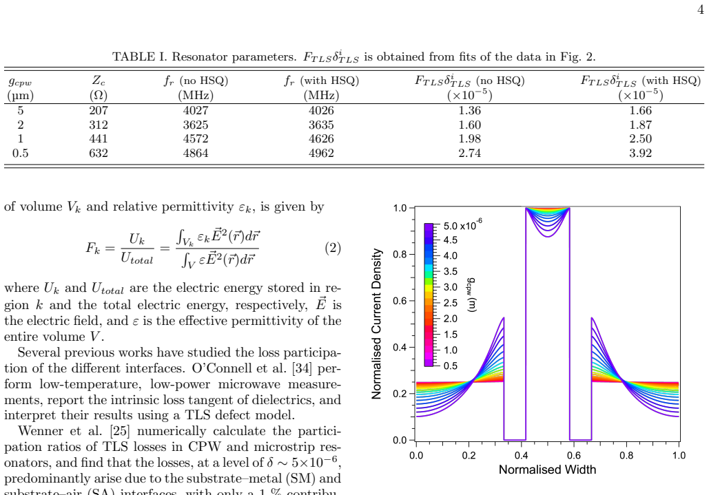
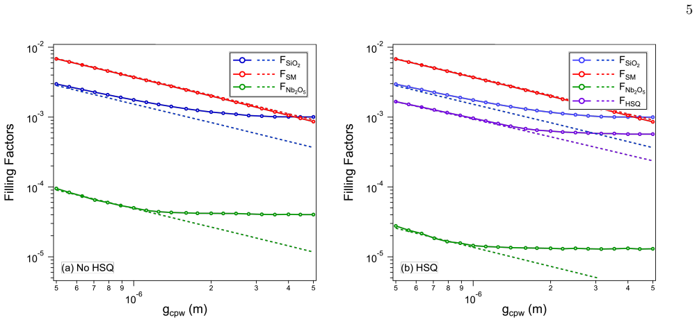
The argument is carried by geometric filling factors, $F_k = U_k / U_{\mathrm{total}}$, the fraction of stored electric energy in each lossy region, computed from 3D finite-element solutions of the Maxwell–London equations. Because the disordered NbN film has a magnetic penetration depth of roughly $1\,\mu\mathrm{m}$, comparable to the device dimensions, the superconductor is modelled by a complex permittivity in the dirty local limit, and electrostatic simulations are shown to give the wrong filling factors. These $F_k$ feed the linear decomposition $1/Q_{\mathrm{TLS}} = \sum_k F_k \delta^i_k$, which converts measured total TLS loss into the intrinsic loss tangent of each region and singles out HSQ as the largest term.
What would settle it
Take finished resonators that still carry HSQ, remove the HSQ with a dedicated strip process, and remeasure the single-photon TLS loss; if the loss does not drop by the amount predicted from $F_{\mathrm{HSQ}} \times 8.0 \times 10^{-3}$, the dominance claim is wrong. Alternatively, measure the HSQ loss tangent directly in a resonator whose filling factor is fixed by geometry alone, such as a lumped-element capacitor with the HSQ as the known dielectric.
Extended reading notes
Core claim
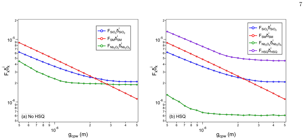
On the paper's own terms, the central discovery is that HSQ is the dominant TLS loss channel in superconducting NbN coplanar waveguide resonators whenever it is left on the device, and that its intrinsic loss tangent is $\delta^i_{\mathrm{HSQ}} = 8.0 \times 10^{-3}$. This is roughly four times the loss tangent of the silicon-oxide interfaces that have historically been blamed for surface losses, so the standard assumption that a spin-on-glass resist behaves like silicon oxide would seriously underestimate its impact. The dominance is not because HSQ is extraordinarily lossy per volume, but because it sits directly above the center conductor, where the electric field is strongest, so its geometric filling factor is large and grows as the resonator gap shrinks. The paper establishes this by fabricating pairs of resonators that differ only in the HSQ layer, measuring the temperature dependence of the resonance frequency to isolate TLS loss, and using full-wave simulations to convert the measured total loss into per-material loss tangents.
Load-bearing premise
The fitted HSQ loss tangent assumes the device is exactly the modelled stack of uniform dielectric layers with the stated thicknesses and permittivities, with no niobium oxide under the HSQ; if those assumptions miss the real field distribution, the extracted HSQ loss changes even though the measured total loss is unchanged.
Editorial extensions
If this is right
- Leaving HSQ on a finished nanowire resonator sets a floor on the achievable internal quality factor; stripping HSQ after e-beam patterning should raise $Q$ at single-photon powers.
- At sub-micron gaps, the top dielectric's filling factor grows fastest, so high-impedance resonator design must treat the dielectric layer on top of the conductor as a first-order loss term, not a correction.
- Electrostatic filling-factor calculations are not reliable for disordered-superconductor devices whose dimensions are comparable to the magnetic penetration depth; Maxwell–London simulation is needed to separate loss channels.
- The extracted loss tangents of HSQ, substrate-metal interface, niobium oxide, and silicon oxide can be reused as material parameters to predict TLS loss in future nanowire circuits before fabrication.
Reading between the lines
- The extracted HSQ loss tangent inherits the assumed layer stack; if the actual oxide thicknesses or the absence of $\mathrm{Nb_2O_5}$ under HSQ are wrong, the fitted value would compensate. A geometry with a single well-known lossy layer would separate those uncertainties.
- Because developed HSQ is porous amorphous silica, its loss tangent likely depends on exposure dose, development, and baking; the reported value may represent one process condition, so a processing study could find lower-loss HSQ variants.
- The same measurement-and-simulation workflow could rank other nanofabrication resists and hard masks by their predicted TLS loss, giving nanowire developers a screening tool before device fabrication.
Signed reviews
Editorial analysis
A structured set of objections, weighed in public.
Referee Report
Summary. The manuscript reports an experimental and numerical study of two-level-system (TLS) dielectric loss in NbN coplanar waveguide resonators with and without a hydrogen silsesquioxane (HSQ) capping layer on the center conductor. The authors measure the temperature-dependent frequency shift of four resonator geometries (gap widths 0.5–5 µm) at single-photon power and extract the product F_TLS·δ_TLS for each device. They then compute geometric filling factors using 3D finite-element simulations that solve the Maxwell–London equations for the disordered NbN film (penetration depth ≈1 µm), and fit the loss-budget model of Eq. (1) to obtain the intrinsic loss tangents of HSQ, the substrate–metal interface, niobium oxide, and silicon oxide. The central claim, quantified in Table II and stated in Section VI, is that HSQ has δ_i_HSQ = 8.0 × 10⁻³ and, because of its large filling factor, is the dominant TLS loss source in every measured geometry.
Significance. The qualitative result that HSQ increases microwave loss is convincingly established by the paired with/without-HSQ comparison: in each of the four geometries the measured F_TLS·δ_TLS is higher when HSQ is present (Table I), and the frequency-shift method isolates TLS loss from other mechanisms. If the quantitative value for δ_i_HSQ survives further scrutiny, it provides a useful design rule for high-impedance NbN nanowire circuits, where HSQ is commonly left in place. The methodological contribution—using 3D Maxwell–London simulations to account for the large magnetic penetration depth in disordered superconductors when computing participation ratios—is significant and clearly presented. The manuscript also gives credit to prior surface-loss literature and includes sufficient experimental detail for the measurement setup to be reproduced.
major comments (3)
- [Section IV, material-parameter paragraph; Table II] The quantitative extraction of δ_i_HSQ depends critically on the stated assumption: 'Because Nb2O5 requires several days to achieve any meaningful thickness, it is assumed that no Nb2O5 is present underneath the HSQ.' This assumption is load-bearing: the model removes the 5-nm Nb2O5 layer from the center conductor in the HSQ samples and replaces it with HSQ, while the measured with-HSQ loss is only modestly larger than the no-HSQ loss (e.g., 1.66 vs 1.36 × 10⁻⁵ at g_cpw = 5 µm). If a native oxide grows under the HSQ, the fitted δ_i_HSQ would be lower, and the claim of HSQ dominance in the wider geometries could fail. The fabrication sequence leaves the NbN exposed between RIE and HSQ spin with no time specified, and no direct oxide characterization or sensitivity analysis is provided. This issue directly affects the central quantitative claim and should be addressed with, e.g., XPS/TEM cross-section or a sensitivity study varying the under-HSQ oxide thickness.
- [Table II and Fig. 6] The four loss tangents in Table II are obtained by fitting Eq. (1) to the eight F_TLS·δ_TLS values in Table I, yet no uncertainties, covariance, or goodness-of-fit statistics are reported. With four free parameters and eight data points, the fit may not uniquely constrain the individual loss tangents; for instance, δ_i_SM and δ_i_SiO2 both affect the geometry dependence in similar ways. The two-significant-figure value δ_i_HSQ = 8.0 × 10⁻³ therefore conveys a precision that is not supported by the presented analysis. Please report parameter uncertainties (e.g., from a bootstrap or least-squares covariance) and a residual analysis, or explicitly discuss the confidence region for δ_i_HSQ.
- [Section VI and Fig. 7] The conclusion that HSQ is the dominant TLS loss source 'for all dimensions' goes beyond the direct measurements, which show only that HSQ increases loss; the dominance statement is an inference from the fitted parameters. Because the fitted parameters are sensitive to the assumed layer thicknesses, permittivities, and the no-Nb2O5-under-HSQ assumption (as noted above), the dominance claim for the widest geometry (g_cpw = 5 µm) is not yet robust. A sensitivity analysis showing how δ_i_HSQ and the per-region loss contributions in Fig. 7 change under plausible variations of the model parameters would be required to support this strong claim.
minor comments (4)
- [Abstract] The abstract contains an incomplete sentence: 'We emphasise that the loss caused by a spin-on-glass resist such as hydrogen silsesquioxane (HSQ), used for ultrahigh lithographic resolution relevant to the fabrication of nanowires, and find that, when used, HSQ is the dominant source of loss...' The phrase beginning 'the loss caused by...' lacks a main verb. Please rewrite.
- [Section II] The fixed ratio of gap to center conductor width is not stated; please give the ratio (or the center-conductor widths) to make the geometry table self-contained.
- [Section V] In Section V, 'These results confirms' should be 'These results confirm'.
- [Fig. 2 caption] The caption states that the curves are offset by 15 kHz, but does not explain which curves are offset; please clarify the offset convention.
Circularity Check
No significant circularity: the HSQ loss tangent is obtained by fitting Eq. (1) to independent frequency-shift data, and the dominance claim is a post-fit consequence rather than an input.
full rationale
The central quantity, δ_i_HSQ = 8.0 × 10^-3, is not defined in terms of the measured loss or of the paper's own prior results. It is extracted by fitting the linear decomposition 1/Q_TLS = Σ_k F_k δ_i_k, Eq. (1), to the independently measured F_TLS δ_i_TLS values listed in Table I. Those F_TLS δ_i_TLS values are themselves obtained from temperature-dependent frequency-shift measurements analyzed with the standard TLS model of Refs. [35,36]. The filling factors F_k come from 3D finite-element Maxwell–London simulations, which are separate from the loss measurements. The fit has eight measured data points (four geometries, with and without HSQ) and four fitted loss tangents, so the parameters are not forced by construction. The statement that HSQ dominates the loss is a post-fit interpretation of the fitted δ_i_HSQ together with the simulated filling factors, not a prediction that was assumed beforehand. The assumption that no Nb2O5 grows under HSQ is a model-input assumption; it affects the numerical value extracted, but this is a model-sensitivity limitation rather than circular reasoning. Self-citations such as Refs. [4] and [37] are used only for experimental setup details and are not load-bearing for the loss-tangent extraction. The paper also benchmarks its values against external literature, e.g., Refs. [26,28,34,43]. No step in the derivation reduces the claimed result to its own inputs, so the paper is not circular.
Assumptions & free parameters
free parameters (4)
- delta_i_HSQ (HSQ loss tangent) =
8.0 x 10^-3
- delta_i_SM (substrate-metal interface loss tangent) =
1.3 x 10^-3
- delta_i_Nb2O5 (niobium oxide loss tangent) =
4.7 x 10^-2
- delta_i_SiO2 (silicon oxide loss tangent) =
2.1 x 10^-3
assumptions (5)
- domain assumption The TLS tunneling model [35,36] relates the measured frequency shift to the product FTLS*delta_TLS via the digamma-function formula used in Fig. 2.
- domain assumption Total loss is a linear sum of independent lossy regions, Eq. (1).
- domain assumption Each TLS host is a homogeneous dielectric layer of fixed thickness and permittivity: 5 nm SiO2, 5 nm Nb2O5, 2 nm substrate layer, 30 nm HSQ.
- ad hoc to paper No Nb2O5 grows underneath the HSQ-covered center conductor.
- domain assumption NbN's microwave response is described by the local dirty-limit complex permittivity, Eq. (5), with Mattis-Bardeen quasiparticle conductivity.
Cite this review
Pith. "Pith review of Geometric Scaling of Two-Level-System Loss in Superconducting Resonators." pith.science (2026). https://pith.science/paper/TJ2LRBN4
@misc{pith2026190802606,
  author       = {Pith},
  title        = {Pith review of: Geometric Scaling of Two-Level-System Loss in Superconducting Resonators},
  year         = {2026},
  howpublished = {\url{https://pith.science/paper/TJ2LRBN4}},
  note         = {Machine review of arXiv:1908.02606}
}
abstract
We perform an experimental and numerical study of dielectric loss in superconducting microwave resonators at low temperature. Dielectric loss, due to two-level systems, is a limiting factor in several applications, e.g. superconducting qubits, Josephson parametric amplifiers, microwave kinetic-inductance detectors, and superconducting single-photon detectors. Our devices are made of disordered NbN, which, due to magnetic-field penetration, necessitates 3D finite-element simulation of the Maxwell--London equations at microwave frequencies to accurately model the current density and electric field distribution. From the field distribution, we compute the geometric filling factors of the lossy regions in our resonator structures and fit the experimental data to determine the intrinsic loss tangents of its interfaces and dielectrics. We emphasise that the loss caused by a spin-on-glass resist such as hydrogen silsesquioxane (HSQ), used for ultrahigh lithographic resolution relevant to the fabrication of nanowires, and find that, when used, HSQ is the dominant source of loss, with a loss tangent of $\delta^i_{HSQ} = 8 \times 10^{-3}$.
Figures


Figures from the paper (4 more)


Reference graph
Works this paper leans on
-
[1]
Microwave Characterization of Josephson Junction Arrays: Imple- menting a Low Loss Superinductance,
Nicholas A. Masluk, Ioan M. Pop, Archana Kamal, Zlatko K. Minev, and Michel H. Devoret, “Microwave Characterization of Josephson Junction Arrays: Imple- menting a Low Loss Superinductance,” Phys. Rev. Lett. 109, 137002 (2012)
work page 2012
-
[2]
Quantum Superinduc- tor with Tunable Nonlinearity,
M. T. Bell, I. A. Sadovskyy, L. B. Ioffe, A. Yu. Ki- taev, and M. E. Gershenson, “Quantum Superinduc- tor with Tunable Nonlinearity,” Phys. Rev. Lett. 109, 137003 (2012)
work page 2012
-
[3]
Fluxonium: Single Cooper-Pair Circuit Free of Charge Offsets,
Vladimir E. Manucharyan, Jens Koch, Leonid I. Glaz- man, and Michel H. Devoret, “Fluxonium: Single Cooper-Pair Circuit Free of Charge Offsets,” Science 326, 113–116 (2009)
work page 2009
-
[4]
High Kinetic Inductance NbN Nanowire Superinduc- tors,
David Niepce, Jonathan Burnett, and Jonas Bylander, “High Kinetic Inductance NbN Nanowire Superinduc- tors,” Phys. Rev. Appl. 11, 044014 (2019)
work page 2019
-
[5]
High-Kinetic-Inductance Superconduct- ing Nanowire Resonators for Circuit QED in a Magnetic Field,
N. Samkharadze, A. Bruno, P. Scarlino, G. Zheng, D. P. DiVincenzo, L. DiCarlo, and L. M. K. Vandersypen, “High-Kinetic-Inductance Superconduct- ing Nanowire Resonators for Circuit QED in a Magnetic Field,” Phys. Rev. Appl. 5, 044004 (2016)
work page 2016
-
[6]
Aluminium-oxide wires for superconducting high kinetic inductance circuits,
H. Rotzinger, S. T. Skacel, M. Pfirrmann, J. N. Voss, J. M¨ unzberg, S. Probst, P. Bushev, M. P. Weides, A. V. Ustinov, and J. E. Mooij, “Aluminium-oxide wires for superconducting high kinetic inductance circuits,” Super- cond. Sci. Technol. 30, 025002 (2016)
work page 2016
-
[7]
Microres- onators Fabricated from High-Kinetic-Inductance Alu- minum Films,
Wenyuan Zhang, K. Kalashnikov, Wen-Sen Lu, P. Ka- menov, T. DiNapoli, and M. E. Gershenson, “Microres- onators Fabricated from High-Kinetic-Inductance Alu- minum Films,” Phys. Rev. Appl. 11, 011003 (2019)
work page 2019
-
[8]
Granular aluminium as a superconducting mate- rial for high-impedance quantum circuits,
Lukas Gr¨ unhaupt, Martin Spiecker, Daria Gusenkova, Nataliya Maleeva, Sebastian T. Skacel, Ivan Takmakov, Francesco Valenti, Patrick Winkel, Hannes Rotzinger, Wolfgang Wernsdorfer, Alexey V. Ustinov, and Ioan M. Pop, “Granular aluminium as a superconducting mate- rial for high-impedance quantum circuits,” Nat. Mater. , 1 (2019)
work page 2019
Show all 53 references
-
[9]
Strong Coupling Cavity QED with Gate-Defined Double Quantum Dots Enabled by a High Impedance Resonator,
A. Stockklauser, P. Scarlino, J. V. Koski, S. Gasparinetti, C. K. Andersen, C. Reichl, W. Wegscheider, T. Ihn, K. Ensslin, and A. Wallraff, “Strong Coupling Cavity QED with Gate-Defined Double Quantum Dots Enabled by a High Impedance Resonator,” Phys. Rev. X7, 011030 (2017)
2017
-
[10]
Strong spin-photon coupling in silicon,
N. Samkharadze, G. Zheng, N. Kalhor, D. Brousse, A. Sammak, U. C. Mendes, A. Blais, G. Scappucci, and L. M. K. Vandersypen, “Strong spin-photon coupling in silicon,” Science 359, 1123–1127 (2018)
2018
-
[11]
A wideband, low-noise supercon- ducting amplifier with high dynamic range,
Byeong Ho Eom, Peter K. Day, Henry G. LeDuc, and Jonas Zmuidzinas, “A wideband, low-noise supercon- ducting amplifier with high dynamic range,” Nat. Phys. 8, 623 (2012)
2012
-
[12]
Development of a Broadband NbTiN Traveling Wave Parametric Amplifier for MKID Read- out,
C. Bockstiegel, J. Gao, M. R. Vissers, M. Sandberg, S. Chaudhuri, A. Sanders, L. R. Vale, K. D. Irwin, and D. P. Pappas, “Development of a Broadband NbTiN Traveling Wave Parametric Amplifier for MKID Read- out,” J. Low Temp. Phys. 176, 476–482 (2014)
2014
-
[13]
Resonant Phase Matching of Josephson Junction Traveling Wave Parametric Amplifiers,
Kevin O’Brien, Chris Macklin, Irfan Siddiqi, and Xiang Zhang, “Resonant Phase Matching of Josephson Junction Traveling Wave Parametric Amplifiers,” Phys. Rev. Lett. 113, 157001 (2014)
2014
-
[14]
Traveling wave parametric amplifier with Joseph- 8 son junctions using minimal resonator phase matching,
T. C. White, J. Y. Mutus, I.-C. Hoi, R. Barends, B. Campbell, Yu Chen, Z. Chen, B. Chiaro, A. Dunsworth, E. Jeffrey, J. Kelly, A. Megrant, C. Neill, P. J. J. O’Malley, P. Roushan, D. Sank, A. Vainsencher, J. Wenner, S. Chaudhuri, J. Gao, and John M. Marti- nis, “Traveling wave ...
2015
-
[15]
A near–quantum-limited Josephson traveling-wave parametric amplifier,
C. Macklin, K. O’Brien, D. Hover, M. E. Schwartz, V. Bolkhovsky, X. Zhang, W. D. Oliver, and I. Sid- diqi, “A near–quantum-limited Josephson traveling-wave parametric amplifier,” Science 350, 307–310 (2015)
2015
-
[16]
Low-noise kinetic inductance traveling-wave amplifier using three- wave mixing,
M. R. Vissers, R. P. Erickson, H.-S. Ku, Leila Vale, Xian Wu, G. C. Hilton, and D. P. Pappas, “Low-noise kinetic inductance traveling-wave amplifier using three- wave mixing,” Appl. Phys. Lett. 108, 012601 (2016)
2016
-
[17]
Superconducting microwave parametric amplifier based on a quasi-fractal slow propagation line,
A. A. Adamyan, S. E. de Graaf, S. E. Kubatkin, and A. V. Danilov, “Superconducting microwave parametric amplifier based on a quasi-fractal slow propagation line,” J. Appl. Phys. 119, 083901 (2016)
2016
-
[18]
Power Han- dling and Responsivity of Submicron Wide Supercon- ducting Coplanar Waveguide Resonators,
R. M. J. Janssen, A. Endo, J. J. A. Baselmans, P. J. de Visser, R. Barends, and T. M. Klapwijk, “Power Han- dling and Responsivity of Submicron Wide Supercon- ducting Coplanar Waveguide Resonators,” J. Low Temp. Phys. 167, 354–359 (2012)
2012
-
[19]
Operation of a Superconducting Nanowire in Two Detection Modes: KID and SPD,
Edward Schroeder, Philip Mauskopf, Hamdi Mani, Sean Bryan, Karl K. Berggren, and Di Zhu, “Operation of a Superconducting Nanowire in Two Detection Modes: KID and SPD,” J. Low Temp. Phys. 194, 386–393 (2019)
2019
-
[20]
Demonstration of Microwave Multiplexed Readout of DC-Biased Superconducting Nanowire Detectors,
A. K. Sinclair, E. Schroeder, D. Zhu, M. Colangelo, J. Glasby, P. D. Mauskopf, H. Mani, and K. K. Berggren, “Demonstration of Microwave Multiplexed Readout of DC-Biased Superconducting Nanowire Detectors,” IEEE Trans. Appl. Supercond. 29, 1–4 (2019)
2019
-
[21]
Interacting two-level defects as sources of fluctuating high-frequency noise in supercon- ducting circuits,
Clemens M¨ uller, J¨ urgen Lisenfeld, Alexander Shnirman, and Stefano Poletto, “Interacting two-level defects as sources of fluctuating high-frequency noise in supercon- ducting circuits,” Phys. Rev. B 92, 035442 (2015)
2015
-
[22]
Fluctuations of Energy-Relaxation Times in Superconducting Qubits,
P. V. Klimov, J. Kelly, Z. Chen, M. Neeley, A. Megrant, B. Burkett, R. Barends, K. Arya, B. Chiaro, Yu Chen, A. Dunsworth, A. Fowler, B. Foxen, C. Gidney, M. Giustina, R. Graff, T. Huang, E. Jeffrey, Erik Lucero, J. Y. Mutus, O. Naaman, C. Neill, C. Quin- tana, P. Roushan, Danie...
2018
-
[23]
Correlating decoherence in transmon qubits: Low frequency noise by single fluctuators,
Steffen Schl¨ or, J¨ urgen Lisenfeld, Clemens M¨ uller, Alexander Bilmes, Andre Schneider, David P. Pappas, Alexey V. Ustinov, and Martin Weides, “Correlating decoherence in transmon qubits: Low frequency noise by single fluctuators,” arXiv (2019), 1901.05352
2019 arXiv
-
[24]
Decoherence benchmarking of super- conducting qubits,
Jonathan J. Burnett, Andreas Bengtsson, Marco Scigli- uzzo, David Niepce, Marina Kudra, Per Delsing, and Jonas Bylander, “Decoherence benchmarking of super- conducting qubits,” npj Quantum Inf. 5, 54 (2019)
2019
-
[25]
Surface loss simulations of superconducting coplanar waveguide resonators,
J. Wenner, R. Barends, R. C. Bialczak, Yu Chen, J. Kelly, Erik Lucero, Matteo Mariantoni, A. Megrant, P. J. J. O’Malley, D. Sank, A. Vainsencher, H. Wang, T. C. White, Y. Yin, J. Zhao, A. N. Cleland, and John M. Martinis, “Surface loss simulations of superconducting coplanar w...
2011
-
[26]
Sur- face participation and dielectric loss in superconducting qubits,
C. Wang, C. Axline, Y. Y. Gao, T. Brecht, Y. Chu, L. Frunzio, M. H. Devoret, and R. J. Schoelkopf, “Sur- face participation and dielectric loss in superconducting qubits,” Appl. Phys. Lett. 107, 162601 (2015)
2015
-
[27]
Bulk and surface loss in superconducting transmon qubits,
Oliver Dial, Douglas T. McClure, Stefano Poletto, G. A. Keefe, Mary Beth Rothwell, Jay M. Gambetta, David W. Abraham, Jerry M. Chow, and Matthias Steffen, “Bulk and surface loss in superconducting transmon qubits,” Supercond. Sci. Technol. 29, 044001 (2016)
2016
-
[28]
Analysis and mitigation of interface losses in trenched superconducting coplanar waveguide resonators,
G. Calusine, A. Melville, W. Woods, R. Das, C. Stull, V. Bolkhovsky, D. Braje, D. Hover, D. K. Kim, X. Miloshi, D. Rosenberg, A. Sevi, J. L. Yoder, E. Dauler, and W. D. Oliver, “Analysis and mitigation of interface losses in trenched superconducting coplanar waveguide resonato...
2018
-
[29]
Determining Interface Dielectric Losses in Su- perconducting Coplanar-Waveguide Resonators,
W. Woods, G. Calusine, A. Melville, A. Sevi, E. Golden, D. K. Kim, D. Rosenberg, J. L. Yoder, and W. D. Oliver, “Determining Interface Dielectric Losses in Su- perconducting Coplanar-Waveguide Resonators,” Phys. Rev. Appl. 12, 014012 (2019)
2019
-
[30]
Effects of developing conditions on the contrast and sensitivity of hydrogen silsesquioxane,
Yifang Chen, Haifang Yang, and Zheng Cui, “Effects of developing conditions on the contrast and sensitivity of hydrogen silsesquioxane,” Microelectron. Eng. 83, 1119– 1123 (2006)
2006
-
[31]
Nano-patterning of a hydrogen silsesquioxane resist with reduced linewidth fluctua- tions,
H. Namatsu, T. Yamaguchi, M. Nagase, K. Yamazaki, and K. Kurihara, “Nano-patterning of a hydrogen silsesquioxane resist with reduced linewidth fluctua- tions,” Microelectron. Eng. 41-42, 331–334 (1998)
1998
-
[32]
The effects of plasma treatment for low dielectric constant hydrogen silsesquioxane (HSQ),
P. T. Liu, T. C. Chang, S. M. Sze, F. M. Pan, Y. J. Mei, W. F. Wu, M. S. Tsai, B. T. Dai, C. Y. Chang, F. Y. Shih, and H. D. Huang, “The effects of plasma treatment for low dielectric constant hydrogen silsesquioxane (HSQ),” Thin Solid Films 332, 345–350 (1998)
1998
-
[33]
Contribution of dielectrics to frequency and noise of NbTiN superconducting resonators,
R. Barends, H. L. Hortensius, T. Zijlstra, J. J. A. Basel- mans, S. J. C. Yates, J. R. Gao, and T. M. Klapwijk, “Contribution of dielectrics to frequency and noise of NbTiN superconducting resonators,” Appl. Phys. Lett. 92, 223502 (2008)
2008
-
[34]
Microwave dielectric loss at single pho- ton energies and millikelvin temperatures,
Aaron D. O’Connell, M. Ansmann, R. C. Bialczak, M. Hofheinz, N. Katz, Erik Lucero, C. McKenney, M. Neeley, H. Wang, E. M. Weig, A. N. Cleland, and J. M. Martinis, “Microwave dielectric loss at single pho- ton energies and millikelvin temperatures,” Appl. Phys. Lett. 92, 112903 (2008)
2008
-
[35]
Experimental evidence for a surface distribution of two- level systems in superconducting lithographed microwave resonators,
Jiansong Gao, Miguel Daal, Anastasios Vayonakis, Shwe- tank Kumar, Jonas Zmuidzinas, Bernard Sadoulet, Ben- jamin A. Mazin, Peter K. Day, and Henry G. Leduc, “Experimental evidence for a surface distribution of two- level systems in superconducting lithographed microwave reson...
2008
-
[36]
Properties of supercon- ducting planar resonators at millikelvin temperatures,
T. Lindstr¨ om, J. E. Healey, M. S. Colclough, C. M. Muir- head, and A. Ya. Tzalenchuk, “Properties of supercon- ducting planar resonators at millikelvin temperatures,” Phys. Rev. B 80, 132501 (2009)
2009
-
[37]
Noise and loss of superconduct- ing aluminium resonators at single photon energies,
Jonathan Burnett, Andreas Bengtsson, David Niepce, and Jonas Bylander, “Noise and loss of superconduct- ing aluminium resonators at single photon energies,” J. Phys. Conf. Ser. 969, 012131 (2018)
2018
-
[38]
Efficient and robust analysis of complex scattering data under noise in microwave resonators,
S. Probst, F. B. Song, P. A. Bushev, A. V. Ustinov, and M. Weides, “Efficient and robust analysis of complex scattering data under noise in microwave resonators,” Rev. Sci. Instrum. 86, 024706 (2015)
2015
-
[39]
Substrate surface engineering for high-quality sili- con/aluminum superconducting resonators,
C. T. Earnest, J. H. B´ ejanin, T. G. McConkey, E. A. Peters, A. Korinek, H. Yuan, and M. Mariantoni, “Substrate surface engineering for high-quality sili- con/aluminum superconducting resonators,” Supercond. Sci. Technol. 31, 125013 (2018)
2018
-
[40]
Investigat- ing Surface Loss Effects in Superconducting Transmon Qubits,
Jay M. Gambetta, Conal E. Murray, Y.-K.-K. Fung, Douglas T. McClure, Oliver Dial, William Shanks, Jef- 9 frey W. Sleight, and Matthias Steffen, “Investigat- ing Surface Loss Effects in Superconducting Transmon Qubits,” IEEE Trans. Appl. Supercond. 27, 1–5 (2017)
2017
-
[41]
Growth of native oxide on a silicon sur- face,
M. Morita, T. Ohmi, E. Hasegawa, M. Kawakami, and M. Ohwada, “Growth of native oxide on a silicon sur- face,” J. Appl. Phys. 68, 1272–1281 (1990)
1990
-
[42]
Degradation of Super- conducting Nb/NbN Films by Atmospheric Oxidation,
M. David Henry, Steve Wolfley, Travis Young, Todd Monson, Charles J. Pearce, Rupert Lewis, Blythe Clark, Lyle Brunke, and Nancy Missert, “Degradation of Super- conducting Nb/NbN Films by Atmospheric Oxidation,” IEEE Trans. Appl. Supercond. 27, 1–5 (2017)
2017
-
[43]
Measurement of dielec- tric losses in amorphous thin films at gigahertz frequen- cies using superconducting resonators,
Ch Kaiser, S. T. Skacel, S. W¨ unsch, R. Dolata, B. Mack- rodt, A. Zorin, and M. Siegel, “Measurement of dielec- tric losses in amorphous thin films at gigahertz frequen- cies using superconducting resonators,” Supercond. Sci. Technol. 23, 075008 (2010)
2010
-
[44]
Understanding Qual- ity Factor Degradation in Superconducting Niobium Cavities at Low Microwave Field Amplitudes,
A. Romanenko and D. I. Schuster, “Understanding Qual- ity Factor Degradation in Superconducting Niobium Cavities at Low Microwave Field Amplitudes,” Phys. Rev. Lett. 119, 264801 (2017)
2017
-
[45]
Supercon- ducting properties and Hall effect of epitaxial NbN thin films,
S. P. Chockalingam, Madhavi Chand, John Jesudasan, Vikram Tripathi, and Pratap Raychaudhuri, “Supercon- ducting properties and Hall effect of epitaxial NbN thin films,” Phys. Rev. B 77, 214503 (2008)
2008
-
[46]
Electrodynamics of Metallic Supercon- ductors,
M. Dressel, “Electrodynamics of Metallic Supercon- ductors,” Adv. Condens. Matter Phys. 2013 (2013), 10.1155/2013/104379
2013 doi
-
[47]
Microscopic derivation of the ginzburg- landau equations in the theory of superconductivity,
L. P. Gor’kov, “Microscopic derivation of the ginzburg- landau equations in the theory of superconductivity,” JETP 9, 1364 (1959)
1959
-
[48]
Tinkham, Introduction to Superconductivity (Dover Books, 2004)
M. Tinkham, Introduction to Superconductivity (Dover Books, 2004)
2004
-
[49]
Phase Fluctuations in a Strongly Disordered s- Wave NbN Superconductor Close to the Metal-Insulator Transition,
Mintu Mondal, Anand Kamlapure, Madhavi Chand, Garima Saraswat, Sanjeev Kumar, John Jesudasan, L. Benfatto, Vikram Tripathi, and Pratap Raychaud- huri, “Phase Fluctuations in a Strongly Disordered s- Wave NbN Superconductor Close to the Metal-Insulator Transition,” Phys. Rev. L...
2011
-
[50]
Superconducting Parameters and Size Effects of Aluminum Films and Foils,
M. David Maloney, Francisco de la Cruz, and Manuel Cardona, “Superconducting Parameters and Size Effects of Aluminum Films and Foils,” Phys. Rev. B 5, 3558– 3572 (1972)
1972
-
[51]
Magnetic penetration depth measurements of superconducting thin films by a microstrip resonator technique,
B. W. Langley, S. M. Anlage, R. F. W. Pease, and M. R. Beasley, “Magnetic penetration depth measurements of superconducting thin films by a microstrip resonator technique,” Rev. Sci. Instrum. 62, 1801–1812 (1991)
1991
-
[52]
Empirical model of the microwave properties of high- temperature superconductors,
O. G. Vendik, I. B. Vendik, and D. I. Kaparkov, “Empirical model of the microwave properties of high- temperature superconductors,” IEEE Trans. Microwave Theory Tech. 46, 469–478 (1998)
1998
-
[53]
Nonlinear Circuit Model for Discontinuity of Step in Width in Superconducting Mi- crostrip Structures and Its Impact on Nonlinear Effects,
S. Mohammad Hassan Javadzadeh, Forouhar Farzaneh, and Mehdi Fardmanesh, “Nonlinear Circuit Model for Discontinuity of Step in Width in Superconducting Mi- crostrip Structures and Its Impact on Nonlinear Effects,” IEEE Trans. Appl. Supercond. 23, 1301208 (2013)
2013
Reviewed August 14, 2026 · model on record in the stance chip above.
Discussion (0). Continue with ORCID to comment.