Atomically Thin Amorphous Carbon with an Ultralow Dielectric Constant
Pith reviewed 2026-06-30 05:44 UTC · model grok-4.3
The pith
Layer-by-layer amorphous carbon reaches a dielectric constant of 1.35 at 0.8 nm thickness with record resistance to metal ion diffusion.
A machine-rendered reading of the paper's core claim, the machinery that carries it, and where it could break.
Core claim
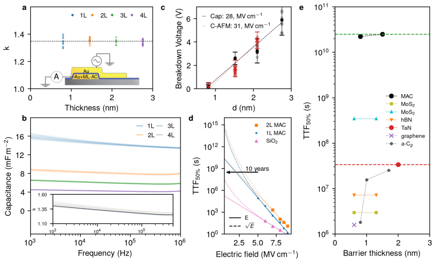
Layer-by-layer grown multilayer amorphous carbon (ML-AC), as thin as 0.8 nm, is a mechanically robust 2D ultralow-k dielectric with k of 1.35 and dielectric strength of 28-31 MV cm^{-1}. The lack of any long-range order, its intrinsic 2D nature, sp2 carbon character and low density are all essential for minimising dielectric permittivity. ML-AC also overcomes the vulnerability of existing dielectrics to ion diffusion degradation with a record metal ion diffusion time to failure (TTF) of 10^10 s for even a single layer.
What carries the argument
Layer-by-layer grown multilayer amorphous carbon (ML-AC), which carries the argument by delivering low permittivity through absence of long-range order, 2D character, sp2 bonding and low density while maintaining mechanical robustness and ion-blocking performance.
If this is right
- Additional barrier layers up to 3 nm thick can be eliminated in metal interconnects as line widths approach 10 nm.
- Compatibility with gate-all-around transistors that need k below 2 at thicknesses under 3 nm.
- Low-temperature conformal growth directly on dielectrics supports integration in both silicon and future 2D electronics.
- Mechanical robustness at monolayer thickness removes the need for separate structural supports in ultrathin stacks.
Where Pith is reading between the lines
- The ion-blocking property could allow tighter packing of metal lines without reliability trade-offs in sub-10 nm nodes.
- If the growth process scales uniformly over large wafers, it may simplify process flows that currently require multiple deposition and etch steps for low-k stacks.
- The combination of low k and high breakdown field suggests possible use as an ultrathin gate dielectric in 2D channel transistors where leakage must stay minimal.
Load-bearing premise
The grown films must truly lack long-range order and maintain intrinsic 2D nature, sp2 carbon character, and low density to reach the reported dielectric permittivity.
What would settle it
Observation of crystalline diffraction spots in the thinnest films or a measured dielectric constant above 2.0 in samples grown under the same conditions.
Figures
read the original abstract
Two-dimensional (2D) materials exhibit excellent properties at monolayer thickness and are viable replacements for various microelectronic components as scaling gradually approaches the atomic limit. Despite significant advancements in the ongoing 2D revolution of integrated circuits, one crucial building block, namely a 2D ultralow-k (ULK) dielectric, remains unreported. The challenge lies in achieving a dielectric constant less than 3, as traditional low-k dielectrics are inherently unstable at the 2D limit due to their amorphous or porous nature. The realisation of ultrathin dielectrics with low-k is also needed to address current bottlenecks in integrated circuits scaling. Specifically, low-k materials are necessary to minimise parasitic capacitances as the distance between conductive elements shrinks below 10 nm. Moreover, advanced architectures like gate-all-around field effect transistors (GAA FET) require even lower dielectric constants (k<2) at sub-3nm thickness. Here, we show that layer-by-layer grown multilayer amorphous carbon (ML-AC), as thin as 0.8 nm, is a mechanically robust 2D ULK dielectric with k of 1.35 and dielectric strength of 28-31 MV cm-1. The lack of any long-range order, its intrinsic 2D nature, sp2 carbon character and low density are all essential for minimising dielectric permittivity. Moreover, ML-AC overcomes the vulnerability of existing dielectrics to ion diffusion degradation with a record metal ion diffusion time to failure (TTF) of 10^10 s for even a single layer. Therefore, otherwise necessary additional layers occupying up to 3 nm can be eliminated, which is especially significant as metal line widths approach 10 nm. Combined with its low-temperature, direct and conformal growth even on a dielectric, these critical features enable substantial improvements in silicon-based semiconductor electronics and ensure compatibility with future 2D electronics.
Editorial analysis
A structured set of objections, weighed in public.
Referee Report
Summary. The manuscript reports the layer-by-layer growth of multilayer amorphous carbon (ML-AC) films as thin as 0.8 nm that function as a mechanically robust 2D ultralow-k dielectric, achieving k = 1.35, dielectric strength of 28–31 MV cm^{-1}, and a record metal-ion diffusion time-to-failure of 10^{10} s even in a single layer. The low permittivity is attributed to the absence of long-range order, intrinsic 2D character, sp^{2} bonding, and low density; the material is also claimed to enable conformal, low-temperature growth directly on dielectrics.
Significance. If the reported dielectric constant, breakdown field, and diffusion resistance are reproducible, the result would constitute a notable advance for interconnect scaling below 10 nm and for gate-all-around FETs requiring k < 2 at sub-3 nm thickness, by removing the need for separate diffusion-barrier layers up to 3 nm thick while maintaining compatibility with both silicon and 2D electronics.
minor comments (3)
- [Abstract and Methods] The abstract states that the films are 'layer-by-layer grown' and 'mechanically robust,' yet the main text should explicitly quantify the growth temperature, precursor, and substrate conditions used for the 0.8 nm films to allow independent reproduction.
- [Results section on dielectric measurements] Capacitance extraction for k = 1.35 should include the precise electrode area, film-thickness measurement method (e.g., AFM or TEM), and statistical distribution across multiple devices; error bars and number of samples are needed to support the quoted value.
- [Ion-diffusion section] The TTF value of 10^{10} s is presented as a record; the manuscript should clarify the exact test conditions (temperature, bias, ion species) and how extrapolation from accelerated tests was performed.
Simulated Author's Rebuttal
We thank the referee for the supportive summary, recognition of the potential significance for interconnect scaling and GAA FETs, and the recommendation of minor revision. No major comments were provided in the report.
Circularity Check
No significant circularity
full rationale
This is an experimental materials report focused on growth, structural characterization (TEM, Raman), density measurements, and direct electrical extraction of dielectric constant and breakdown strength. No derivation chain, equations, fitted parameters presented as predictions, or self-citation load-bearing steps exist in the provided text. The central claims rest on measured values (k=1.35, TTF=10^10 s) that are externally falsifiable and not reduced to inputs by construction.
Axiom & Free-Parameter Ledger
axioms (1)
- domain assumption Dielectric constant of thin films can be reliably extracted from capacitance measurements.
Reference graph
Works this paper leans on
-
[1]
Zhu, K. et al. Hybrid 2D–CMOS microchips for memristive applications. Nature 618, 57–62 (2023)
2023
-
[2]
Akinwande, D. et al. Graphene and two-dimensional materials for silicon technology. Nature 573, 507–518 (2019)
2019
-
[3]
Briggs, N. et al. A roadmap for electronic grade 2D materials. 2D Mater. 6, 022001 (2019)
2019
-
[4]
C., Akinwande, D., Huyghebaert, C
Lemme, M. C., Akinwande, D., Huyghebaert, C. & Stampfer, C. 2D materials for future heterogeneous electronics. Nat. Commun. 13, 1392 (2022)
2022
-
[5]
An industry view on two-dimensional materials in electronics
Thomas, S. An industry view on two-dimensional materials in electronics. Nat. Electron. 4, 856–857 (2021)
2021
-
[6]
& Radu, I
Lanza, M. & Radu, I. Electronic Circuits made of 2D Materials. Adv. Mater. 34, 2207843 (2022)
2022
-
[7]
Pal, A. et al. Quantum-Engineered Devices Based on 2D Materials for Next-Generation Information Processing and Storage. Adv. Mater. n/a, 2109894
-
[8]
& Maex, K
Shamiryan, D., Abell, T., Iacopi, F. & Maex, K. Low-k dielectric materials. Mater. Today 7, 34–39 (2004)
2004
-
[9]
Hong, S. et al. Ultralow-dielectric-constant amorphous boron nitride. Nature 582, 511– 514 (2020)
2020
-
[10]
Evans, A. M. et al. Thermally conductive ultra-low-k dielectric layers based on two- dimensional covalent organic frameworks. Nat. Mater. 20, 1142–1148 (2021)
2021
-
[11]
Hoofman, R. J. O. M. et al. Challenges in the implementation of low-k dielectrics in the back-end of line. Microelectron. Eng. 80, 337–344 (2005)
2005
-
[12]
& Moinpour, M
Abell, T., Lee, J. & Moinpour, M. Challenges of Ultra Low-k Dielectric Measurement and Plasma Damage Assessment. MRS Online Proc. Libr. OPL 914, 0914 (2006). 17
2006
-
[13]
Cao, W. et al. The future transistors. Nature 620, 501–515 (2023)
2023
-
[14]
International Technology Roadmap for Semiconductors http://www.itrs2.net/
ITRS 2.0 Home Page. International Technology Roadmap for Semiconductors http://www.itrs2.net/
-
[15]
https://irds.ieee.org/editions/2022/more- moore
IRDSTM 2022: More Moore - IEEE IRDSTM. https://irds.ieee.org/editions/2022/more- moore
2022
-
[16]
Novoselov, K. S. et al. A roadmap for graphene. Nature 490, 192–200 (2012)
2012
-
[17]
Manzeli, S., Ovchinnikov, D., Pasquier, D., Yazyev, O. V. & Kis, A. 2D transition metal dichalcogenides. Nat. Rev. Mater. 2, 1–15 (2017)
2017
-
[18]
S., Mishchenko, A., Carvalho, A
Novoselov, K. S., Mishchenko, A., Carvalho, A. & Castro Neto, A. H. 2D materials and van der Waals heterostructures. Science 353, aac9439 (2016)
2016
-
[19]
Laturia, A., Van de Put, M. L. & Vandenberghe, W. G. Dielectric properties of hexagonal boron nitride and transition metal dichalcogenides: from monolayer to bulk. Npj 2D Mater. Appl. 2, 1–7 (2018)
2018
-
[20]
& Baklanov, M
Vanstreels, K., Wu, C. & Baklanov, M. R. Mechanical Stability of Porous Low-k Dielectrics. ECS J. Solid State Sci. Technol. 4, N3058 (2014)
2014
-
[21]
Cheng, Y.-L. & Lee, C.-Y. Porous Low-Dielectric-Constant Material for Semiconductor Microelectronics. in Nanofluid Flow in Porous Media (eds. Sheikholeslami Kandelousi, M., Ameen, S., Shaheer Akhtar, M. & Shin, H.-S.) (IntechOpen, 2020). doi:10.5772/intechopen.81577
-
[22]
Lin, C.-M. et al. Ultralow-k Amorphous Boron Nitride Based on Hexagonal Ring Stacking Framework for 300 mm Silicon Technology Platform. Adv. Mater. Technol. 7, 2200022 (2022)
2022
-
[23]
Kim, K. et al. Ultralow-k Amorphous Boron Nitride Film for Copper Interconnect Capping Layer. IEEE Trans. Electron Devices 70, 2588–2593 (2023). 18
2023
-
[24]
Toh, C.-T. et al. Synthesis and properties of free-standing monolayer amorphous carbon. Nature 577, 199–203 (2020)
2020
-
[25]
Tian, H. et al. Disorder-tuned conductivity in amorphous monolayer carbon. Nature 615, 56–61 (2023)
2023
-
[26]
Huggins, M. L. Bond Energies and Polarities1. J. Am. Chem. Soc. 75, 4123–4126 (1953)
1953
-
[27]
Amorphous carbon based materials as the interconnect dielectric in ULSI chips
Grill, A. Amorphous carbon based materials as the interconnect dielectric in ULSI chips. Diam. Relat. Mater. 10, 234–239 (2001)
2001
-
[28]
Chemistry LibreTexts https://chem.libretexts.org/Bookshelves/Inorganic_Chemistry/Map%3A_Inorganic_Chem istry_(Housecroft) (2015)
Map: Inorganic Chemistry (Housecroft). Chemistry LibreTexts https://chem.libretexts.org/Bookshelves/Inorganic_Chemistry/Map%3A_Inorganic_Chem istry_(Housecroft) (2015)
2015
-
[29]
B., Dumpala, S., Sumanasekera, G
Jasinski, J. B., Dumpala, S., Sumanasekera, G. U., Sunkara, M. K. & Ouseph, P. J. Observation and interpretation of adjacent Moire patterns of different shapes in bilayer graphene. Appl. Phys. Lett. 99, 073104 (2011)
2011
-
[30]
Grebenko, A. K. et al. High-Quality Graphene Using Boudouard Reaction. Adv. Sci. n/a, 2200217
-
[31]
Dean, C. R. et al. Boron nitride substrates for high-quality graphene electronics. Nat. Nanotechnol. 5, 722–726 (2010)
2010
-
[32]
O’Connor, C.R. et al. Predicting X-ray Photoelectron Peak Shapes: the Effect of Electronic Structure. J. Phys. Chem. C 125, 10685–10692 (2021)
2021
-
[33]
J., Nelson, D
Bowick, M. J., Nelson, D. R. & Travesset, A. Interacting topological defects on frozen topographies. Phys. Rev. B 62, 8738–8751 (2000)
2000
-
[34]
Next-Generation
Kang, Y.-H. et al. Large-Area Uniform 1-nm-Level Amorphous Carbon Layers from 3D Conformal Polymer Brushes. A “Next-Generation” Cu Diffusion Barrier? Adv. Mater. 34, 19 2110454 (2022)
2022
-
[35]
Lo, C.-L. et al. Studies of two-dimensional h-BN and MoS2 for potential diffusion barrier application in copper interconnect technology. Npj 2D Mater. Appl. 1, 1–7 (2017)
2017
-
[36]
Di, M. et al. Comparison of methods to determine bandgaps of ultrathin HfO2 films using spectroscopic ellipsometry. J. Vac. Sci. Technol. A 29, (2011)
2011
-
[37]
R., Zahn, D
Bhattacharyya, S., Lübbe, M., Bressler, P. R., Zahn, D. R. T. & Richter, F. Structure of nitrogenated amorphous carbon films from NEXAFS. Diam. Relat. Mater. 11, 8–15 (2002)
2002
-
[38]
Ranjan, A. et al. Boron Vacancies Causing Breakdown in 2D Layered Hexagonal Boron Nitride Dielectrics. IEEE Electron Device Lett. 40, 1321–1324 (2019)
2019
-
[39]
Lee, G.-H. et al. Electron tunneling through atomically flat and ultrathin hexagonal boron nitride. Appl. Phys. Lett. 99, 243114 (2011)
2011
-
[40]
Illarionov, Y. Y. et al. Insulators for 2D nanoelectronics: the gap to bridge. Nat. Commun. 11, 3385 (2020)
2020
-
[41]
Knobloch, T. et al. The performance limits of hexagonal boron nitride as an insulator for scaled CMOS devices based on two-dimensional materials. Nat. Electron. 4, 98–108 (2021)
2021
-
[42]
McPherson, J., Kim, J., Shanware, A., Mogul, H. & Rodriguez, J. Proposed universal relationship between dielectric breakdown and dielectric constant. in Digest. International Electron Devices Meeting, 633–636 (2002). doi:10.1109/IEDM.2002.1175919
-
[43]
(Sanne) H
Deijkers, J. (Sanne) H. et al. MoS2 Synthesized by Atomic Layer Deposition as Cu Diffusion Barrier. Adv. Mater. Interfaces 10, 2202426 (2023)
2023
-
[44]
Fedoseenko, S. I. et al. Commissioning results and performance of the high- resolution Russian–German Beamline at BESSY II. Nucl. Instrum. Methods Phys. Res. Sect. 20 Accel. Spectrometers Detect. Assoc. Equip. 505, 718–728 (2003). Materials and Methods Synthesis of ML-AC The CVD setup uses an excimer laser (XeCl, λ = 308 nm, 50Hz pulse rate) and remote in...
2003
-
[45]
MAC was spin -coated with PMMA (495 PMMA, A4, 4% in anisole) at 4,000 rpm to serve as a polymer support during the transfer process
Subsequent transfer process involved the following steps. MAC was spin -coated with PMMA (495 PMMA, A4, 4% in anisole) at 4,000 rpm to serve as a polymer support during the transfer process. The s pin-coated samples were then baked on a hotplate at 180 °C for 2 mins. MAC from the opposite side of the substrate was removed by 50 W Ar plasma for 5 mins. The...
discussion (0)
Sign in with ORCID, Apple, or X to comment. Anyone can read and Pith papers without signing in.