REVIEW 3 major objections 5 minor 36 references
Band-pass Magnetic Tunnel Junction based Magnetoresistive Random Access Memory
T0 review · 3 major / 5 minor · reviewed 2026-08-14 · deepseek-v4-flash
Pith's one-line read The paper claims a band-pass spin-filtering superlattice makes STT-MRAM about 1100 percent more energy-efficient than a conventional trilayer magnetic tunnel junction.
desk verdict Coherent transport gives this band-pass MTJ a big simulated energy edge over a trilayer, but the 1100% number is a design ceiling unless dephasing is addressed. read the letter →
The pith
A machine-rendered reading of the paper's core claim, the machinery that carries it, and where it could break.
The reading
What carries the argument
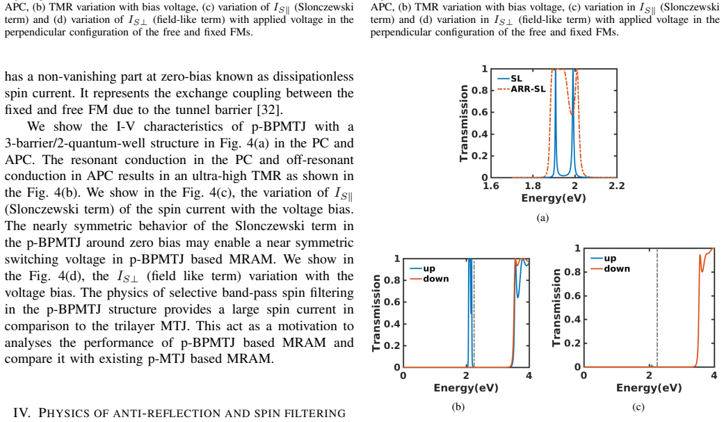
The central object is the band-pass magnetic tunnel junction (BPMTJ): a superlattice of alternating MgO barriers and normal-metal quantum wells, terminated on each side by an anti-reflective region, placed between fixed and free ferromagnets. The anti-reflective region is a normal-metal well of the same width plus a MgO barrier half as wide, which broadens the transmission window just as an anti-reflection coating broadens an optical passband. In the parallel state, up-spin electrons tunnel resonantly near the Fermi level, while in the antiparallel state the spin-dependent band alignment blocks both channels; that contrast is what produces the ultra-high TMR and the large spin current that drives low-voltage switching.
What would settle it
Grow the proposed CoFeB/MgO/NM/MgO/NM/MgO stack with anti-reflective regions and measure the TMR and write switching energy at 300 K as a function of bias; a room-temperature TMR orders of magnitude below $3.5\times10^4\%$, or optimal write energies close to the trilayer values of tens of femtojoules, would directly refute the central claim.
Extended reading notes
Core claim
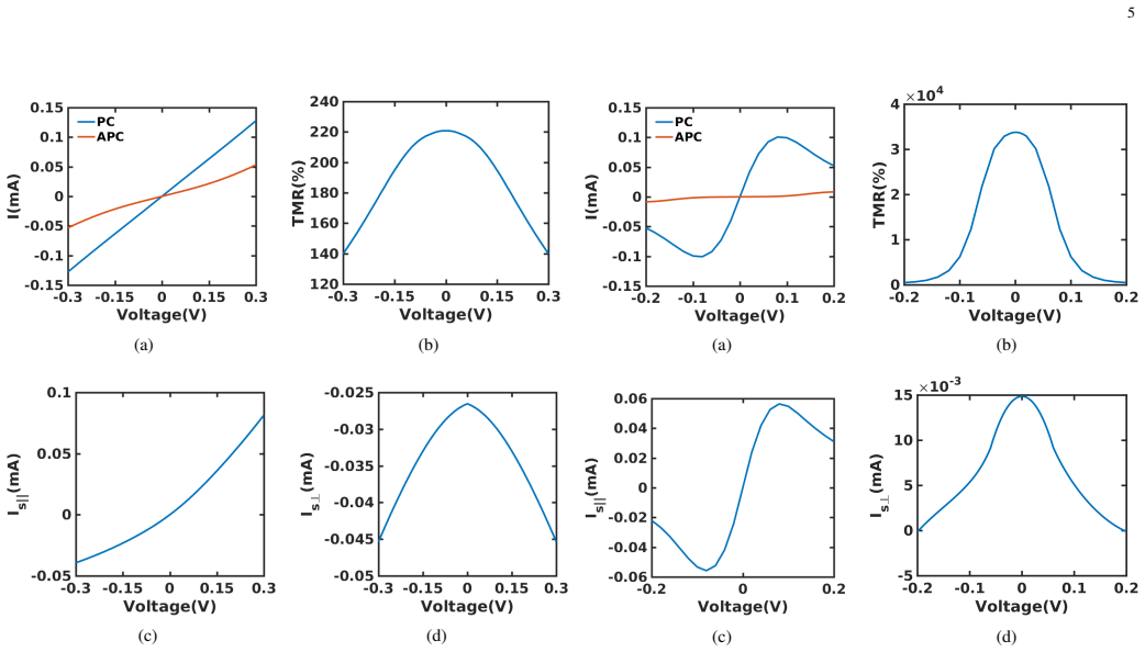
At the paper's center is the claim that coherent band-pass spin filtering, realized by a three-barrier/two-quantum-well MgO/NM superlattice with anti-reflective regions, gives a magnetic tunnel junction a conductance that is strongly spin-selective in the parallel configuration and essentially blocked in the antiparallel configuration. The NEGF-based charge and spin currents, fed self-consistently into the stochastic Landau-Lifshitz-Gilbert-Slonczewski equation at 300 K, predict an ultra-high TMR of about $3.5\times10^4\%$ and a large Slonczewski spin current that switches the free layer at about $\pm 30$ mV. At the optimal operating point the device writes with $5.2$ fJ for P→AP and $1.7$ fJ for AP→P, versus $64$ fJ and $24$ fJ for the trilayer baseline, so the claimed energy saving is 1170% and 1370% in the two directions (rounded to "nearly 1100%" in the abstract). The paper also finds near-symmetric switching voltages, a practical advantage for write circuitry.
Load-bearing premise
The order-of-magnitude energy saving assumes electrons stay phase-coherent through the 3.5 Å metal wells; any room-temperature dephasing from phonons, impurities, or interface roughness could wash out the resonance and erase both the ultra-high TMR and the low write energy.
Editorial extensions
If this is right
- At the simulated optimal operating point, P→AP switching costs $5.2$ fJ instead of $64$ fJ, and AP→P costs $1.7$ fJ instead of $24$ fJ, with switching times near $3$ ns in both designs.
- The BPMTJ's near-symmetric Slonczewski current around zero bias makes the write voltage nearly equal in both directions (about $\pm 30$ mV), unlike the trilayer's asymmetric response.
- The ultra-high TMR of about $3.5\times10^4\%$ gives a much larger read window between the '0' and '1' resistance states.
- Because the benefit comes from the junction structure rather than the free-layer materials, it could be combined with existing perpendicular-anisotropy and scaling improvements.
Reading between the lines
- If the coherent resonance survives dephasing, the same filtering stack could be reused in other spin-torque devices, such as oscillators and sensors that already exploit resonant spin filtering, extending the energy gain beyond memory writes.
- A direct test of the paper's load-bearing assumption would be to add a phase-breaking term to the NEGF calculation and plot TMR versus dephasing strength; that curve would show how quickly the practical advantage disappears at 300 K.
- The paper compares junction-level write energies only; circuit-level overheads such as series resistance, charging, and peripheral write drivers could shrink or enlarge the system-level gain, so the 1100% figure should be read as a device-level rather than chip-level claim.
Signed reviews
Editorial analysis
A structured set of objections, weighed in public.
Referee Report
Summary. The paper proposes a spin-transfer-torque magnetic tunnel junction (STT-MRAM) design based on band-pass spin filtering realized by a MgO/NM superlattice terminated with anti-reflection regions between the fixed and free ferromagnetic layers. Using the non-equilibrium Green's function (NEGF) spin transport formalism coupled self-consistently to the stochastic Landau-Lifshitz-Gilbert-Slonczewski (LLGS) equation, the authors compute I-V characteristics, TMR, spin currents, and switching probability/energy diagrams at 300 K. They report an ultra-high TMR of about 3.5×10^4% and an approximately 1100% improvement in switching energy efficiency over a conventional trilayer MTJ at the optimal operating point, with optimal switching energies of 5.2 fJ (P→AP) and 1.7 fJ (AP→P) versus 64 fJ and 24 fJ for the trilayer device. The parameter set is fully disclosed, and both devices are simulated in the same framework.
Significance. Within the coherent-transport model, the paper is internally consistent and provides a concrete device structure with a full parameter list, a fair trilayer baseline simulated in the same code, and credible macro-spin LLGS dynamics including thermal noise. The strengths are the transparency of the modeling and the direct comparison. If the coherent band-pass resonance survives at room temperature, the design would represent an order-of-magnitude write-energy improvement, which is significant for STT-MRAM. However, the physical plausibility of the central claim depends entirely on the persistence of coherent Fabry-Pérot resonances through atomic-scale metal wells, which the present model assumes but does not test. The lack of any phase-breaking or sensitivity analysis leaves the headline result conditional on an unverified assumption.
major comments (3)
- [Section II, IV; Eq. (2)] The transport model contains no phase-breaking or inelastic scattering in the channel; the self-energies in Eq. (3) are purely contact self-energies. The band-pass transmission and spin-resolved spectra in Fig. 5 are coherent resonances through the superlattice and anti-reflection regions, with NM wells of only 3.5 Å thickness. At room temperature, interface roughness and electron-phonon scattering in such a structure are expected to dephase the resonances, reducing the TMR and spin current that produce the claimed ~1100% energy-efficiency advantage. The authors are aware of phase-breaking from their Ref. [15]; yet no dephasing model or even a stability estimate is presented. Since the central claim sits on this coherence, the manuscript requires either a dephasing sensitivity study or an explicit bound on the tolerable phase-breaking rate before the headline comparison is supportable.
- [Section II and V] Band-pass filtering depends strongly on the exact layer thicknesses: superlattice barrier 1.2 nm, anti-reflection half-barrier 0.6 nm, and NM well 3.5 Å. These dimensions are at the edge of current fabrication control (Refs. [28]-[30]), and a monolayer variation of the well or barrier will shift the resonance condition and potentially destroy the TMR and spin-current advantage. The paper contains no sensitivity analysis for these structural parameters; all energy comparisons in Section V are at the nominal design point. The authors should provide a tolerance study (e.g., ±1 Å on the NM well and barrier widths) and show that the order-of-magnitude energy gain persists.
- [Section V, Fig. 11] The 'optimal operating point' is defined as the intersection of the switching time and switching energy curves. This metric is not justified in the context of memory design, where a write-error-rate target (for example, switching probability ≥ 0.99) and a latency constraint are the usual specifications. A different target probability or a different pulse-width condition would shift the operating point and may change the ratio of energies between BPMTJ and trilayer MTJ. Furthermore, the abstract's 'nearly 1100%' does not match the Section V values of 1170% (P→AP) and 1370% (AP→P). The manuscript should report the switching-energy ratio over a range of pulse widths and probabilities, not only at the single intersection, to substantiate the headline claim.
minor comments (5)
- [Abstract] The TMR is quoted as '3.5*10e4' which is ambiguous; the full text appears to intend 3.5×10^4%. Please correct the formatting.
- [Abstract and Introduction] 'Greens function' is a typo; it should be 'Green's function'.
- [Eq. (15)] The critical current formula as typeset, 'Ic = 2eα ℏ MsV (Hk + Hd 2 )', appears missing the fraction; it should read Ic = (2eα/ℏ) MsV (Hk + Hd/2).
- [Section V] The '5000 iterations' should be clarified as 5000 independent LLGS switching trials; otherwise 'iteration' is ambiguous.
- [Section V] The sentence 'We have removed the zero bias exchange field in all the simulations...' is unclear: if this is done by adding an external field, that field should appear in the LLGS equation; if it is a subtraction of the zero-bias field-like torque, its effect on the trilayer and BPMTJ should be discussed.
Circularity Check
No significant circularity; the energy comparison is a simulation output, with only a transparent design-level dependence on the authors' prior band-pass work.
full rationale
The central derivation is self-contained with respect to the paper's claims. The NEGF Hamiltonian (Eqs. 2-4), current and spin-current operators (Eqs. 7-9), and stochastic LLGS dynamics (Eqs. 10-14) are defined from standard device physics, with material parameters taken from external literature (MgO effective mass 0.18 me, CoFeB-MgO barrier height 0.76 eV, CoFeB exchange splitting 2.15 eV, Fermi energy 2.25 eV, and free-layer parameters from Refs. [20], [24], [27]). The ultra-high TMR (about 3.5e4 percent) and the large spin current are outputs of the transport simulation shown in Figs. 4-5, not fitted constants reused as predictions. The switching-energy comparison in Figs. 10-11 follows from the same transport model coupled to the macrospin LLGS equation with thermal noise, and the trilayer MTJ results are benchmarked against reported switching energies in Refs. [36], [1], [2], providing an external anchor. The only dependence on the authors' prior work is the band-pass/anti-reflection device concept (Ref. [16]); however, the paper re-derives and plots the transmission spectra and spin-resolved transmission in Figs. 4-5 rather than merely importing the result, so the central claim does not reduce to a self-citation. The reliance on coherent resonant transport without dephasing is a real physical robustness concern for room-temperature devices, but it is a correctness/validity risk, not a circularity: the model's assumptions do not include the target energy-efficiency claim. No equation-level or construction-level circularity is present.
Assumptions & free parameters
free parameters (4)
- MgO barrier widths (superlattice barrier 1.2 nm, anti-reflection barrier half-width 0.6 nm) =
1.2 nm / 0.6 nm
- Normal-metal quantum well width =
3.5 angstrom
- Superlattice period count and anti-reflection termination =
3 barriers, 2 wells
- Free layer volume (area 0.25*pi*30^2 nm^2, thickness 1.3 nm) =
30 nm diameter, 1.3 nm thickness
assumptions (6)
- domain assumption Coherent transport with no phase-breaking or inelastic scattering in the MgO/NM superlattice.
- domain assumption Single-band effective-mass and Stoner models represent CoFeB/MgO/NM with the stated parameters.
- domain assumption Transverse modes are uncoupled and parabolic with Et = hbar^2(kx^2+ky^2)/2mFM.
- domain assumption Potential drops linearly across barriers and is flat in metals, with boundary conditions UFixedFM = -qV/2 and UFreeFM = qV/2.
- domain assumption Free-layer magnetization is macro-spin, uniform, with perpendicular anisotropy Hk_perp = 3.3 kOe and volume chosen for thermal stability near 42 kBT.
- domain assumption The anti-reflection design and band-pass filtering from the authors' prior [16] remain valid in the full FM/MgO/NM/MgO stack with FM contacts.
Cite this review
Pith. "Pith review of Band-pass Magnetic Tunnel Junction based Magnetoresistive Random Access Memory." pith.science (2026). https://pith.science/paper/UXFJU5ID
@misc{pith2026190806279,
  author       = {Pith},
  title        = {Pith review of: Band-pass Magnetic Tunnel Junction based Magnetoresistive Random Access Memory},
  year         = {2026},
  howpublished = {\url{https://pith.science/paper/UXFJU5ID}},
  note         = {Machine review of arXiv:1908.06279}
}
read the original abstract
We propose spin transfer torque--magnetoresistive random access memory (STT-MRAM) based on magneto-resistance and spin transfer torque physics of band-pass spin filtering. Utilizing the electronic analogs of optical phenomena such as anti-reflection coating and resonance for spintronic devices, we present the design of an STT-MRAM device with improved features when compared with a traditional trilayer device. The device consists of a superlattice heterostructure terminated with the anti-reflective regions sandwiched between the fixed and free ferromagnetic layers. Employing the Green's function spin transport formalism coupled self-consistently with the stochastic Landau-Lifshitz-Gilbert-Slonczewski equation, we present the design of an STT-MRAM based on the band-pass filtering having an ultra-high TMR (3.5*10e4) and large spin current. We demonstrate that the STT-MRAM design having band-pass spin filtering are nearly 1100% more energy efficient than traditional trilayer magnetic tunnel junction (MTJ) based STT-MRAM. We also present detailed probabilistic switching and energy analysis for a trilayer MTJ and band-pass filtering based STT-MRAM. Our predictions serve as a template to consider the heterostructures for next-generation spintronic device applications.
Figures


Figures from the paper (5 more)


Reference graph
Works this paper leans on
-
[16]
Band-pass Fabry-P `erot magnetic tunnel junctions,
——, “Band-pass Fabry-P `erot magnetic tunnel junctions,” Applied Physics Letters , vol. 112, no. 19, 2018
work page 2018
-
[15]
Role of phase breaking processes on resonant spin transfer torque nano-oscillators,
——, “Role of phase breaking processes on resonant spin transfer torque nano-oscillators,” AIP Advances , vol. 8, no. 5, p. 055913, may 2018
work page 2018
-
[28]
Bias-driven large power microwave emission from MgO-based tunnel magnetoresistance devices,
A. M. Deac, A. Fukushima, H. Kubota, H. Maehara, Y . Suzuki, S. Yuasa, Y . Nagamine, K. Tsunekawa, D. D. Djayaprawira, and N. Watanabe, “Bias-driven large power microwave emission from MgO-based tunnel magnetoresistance devices,” Nature Physics , vol. 4, no. October, pp. 803–809, 2008
work page 2008
-
[30]
S. H. Yang, K. S. Ryu, and S. Parkin, “Domain-wall velocities of up to 750 m s-1 driven by exchange-coupling torque in synthetic antiferromagnets,” Nature Nanotechnology, vol. 10, no. 3, pp. 221–226, 2015
work page 2015
-
[1]
Emerging Memory Technologies: Recent Trends and Prospects,
S. Yu and P. Y . Chen, “Emerging Memory Technologies: Recent Trends and Prospects,” IEEE Solid-State Circuits Magazine , vol. 8, no. 2, pp. 43–56, 2016
work page 2016
-
[2]
An Overview of Nonvolatile Emerging Memories-Spintronics for Working Memories,
T. Endoh, H. Koike, S. Ikeda, T. Hanyu, and H. Ohno, “An Overview of Nonvolatile Emerging Memories-Spintronics for Working Memories,” IEEE Journal on Emerging and Selected Topics in Circuits and Systems , vol. 6, no. 2, pp. 109–119, 2016
work page 2016
-
[3]
Spin- dependent tunneling conductance of Fe|MgO|Fe sandwiches,
W. H. Butler, X.-G. Zhang, T. C. Schulthess, and J. M. MacLaren, “Spin- dependent tunneling conductance of Fe|MgO|Fe sandwiches,” Phys. Rev. B, vol. 63, p. 054416, Jan 2001
work page 2001
-
[4]
Current-driven excitation of magnetic multilayers,
J. C. Slonczewski, “Current-driven excitation of magnetic multilayers,” Journal of Magnetism and Magnetic Materials , vol. 159, no. 1, pp. L1– L7, 1996
work page 1996
Show all 36 references
-
[5]
Emission of spin waves by a magnetic multilayer traversed by a current,
L. Berger, “Emission of spin waves by a magnetic multilayer traversed by a current,” Physical Review B , vol. 54, no. 13, pp. 9353–9358, 1996
1996
-
[6]
Spin transfer torques,
D. Ralph and M. Stiles, “Spin transfer torques,” Journal of Magnetism and Magnetic Materials , vol. 320, no. 7, pp. 1190 – 1216, 2008
2008
-
[7]
Current-induced torques in magnetic materials,
A. Brataas, A. D. Kent, and H. Ohno, “Current-induced torques in magnetic materials,” Nature materials, vol. 11, no. 5, pp. 372–381, 2012
2012
-
[8]
Magnetoresistive Random Access Memory,
D. Apalkov, B. Dieny, and J. M. Slaughter, “Magnetoresistive Random Access Memory,” Proceedings of the IEEE , vol. 104, no. 10, pp. 1796– 1830, 2016
2016
-
[9]
Spin torque switching of 20 nm magnetic tunnel junctions with perpendicular anisotropy,
M. Gajek, J. J. Nowak, J. Z. Sun, P. L. Trouilloud, E. J. O’Sullivan, D. W. Abraham, M. C. Gaidis, G. Hu, S. Brown, Y . Zhu, R. P. Robertazzi, W. J. Gallagher, and D. C. Worledge, “Spin torque switching of 20 nm magnetic tunnel junctions with perpendicular anisotropy,” Applied...
2012
-
[10]
Scalable and thermally robust perpendicular magnetic tunnel junctions for STT-MRAM,
M. Gottwald, J. J. Kan, K. Lee, X. Zhu, C. Park, and S. H. Kang, “Scalable and thermally robust perpendicular magnetic tunnel junctions for STT-MRAM,” Applied Physics Letters , vol. 106, no. 3, 2015
2015
-
[11]
Highly thermally stable sub-20nm magnetic random-access memory based on perpendicular shape anisotropy,
N. Perrissin, S. Lequeux, N. Strelkov, L. Vila, L. Buda-Prejbeanu, S. Auffret, R. C. Sousa, I. L. Prejbeanu, and B. Dieny, “Highly thermally stable sub-20nm magnetic random-access memory based on perpendicular shape anisotropy,” arXiv 1803.02663 , Mar 2018
2018 arXiv
-
[12]
Recent Developments in Perpendicular Mag- netic Anisotropy Thin Films for Data Storage Applications,
B. Tudu and A. Tiwari, “Recent Developments in Perpendicular Mag- netic Anisotropy Thin Films for Data Storage Applications,” V acuum, vol. 146, pp. 329–341, 2017
2017
-
[13]
Ultrasensitive nanoscale magnetic-field sensors based on resonant spin filtering,
A. Sharma, A. Tulapurkar, and B. Muralidharan, “Ultrasensitive nanoscale magnetic-field sensors based on resonant spin filtering,” IEEE Transactions on Electron Devices, vol. 63, no. 11, pp. 4527–4534, 2016
2016
-
[14]
Resonant spin- transfer-torque nano-oscillators,
A. Sharma, A. A. Tulapurkar, and B. Muralidharan, “Resonant spin- transfer-torque nano-oscillators,” Phys. Rev. Applied , vol. 8, p. 064014, Dec 2017
2017
-
[17]
Datta, Electronic transport in mesoscopic systems
S. Datta, Electronic transport in mesoscopic systems . Cambridge University Press, 1997
1997
-
[18]
Cambridge University Press, 2005
——, Quantum transport: Atom to Transistor . Cambridge University Press, 2005
2005
-
[19]
Quantum transport with spin dephasing: A nonequlibrium Green’s function approach,
A. A. Yanik, G. Klimeck, and S. Datta, “Quantum transport with spin dephasing: A nonequlibrium Green’s function approach,” Physical Review B, vol. 76, no. 4, p. 045213, 2007
2007
-
[20]
V oltage asym- metry of spin-transfer torques,
D. Datta, B. Behin-Aein, S. Datta, and S. Salahuddin, “V oltage asym- metry of spin-transfer torques,” Nanotechnology, IEEE Transactions on , vol. 11, no. 2, pp. 261–272, 2012
2012
-
[21]
Modeling of nanoscale devices,
M. Anantram, M. S. Lundstrom, and D. E. Nikonov, “Modeling of nanoscale devices,” Proceedings of the IEEE , vol. 96, no. 9, pp. 1511– 1550, 2008
2008
-
[22]
Quantum transport simulation of tunneling based spin torque transfer (STT) devices: Design trade offs and torque efficiency,
S. Salahuddin, D. Datta, P. Srivastava, and S. Datta, “Quantum transport simulation of tunneling based spin torque transfer (STT) devices: Design trade offs and torque efficiency,” Proceedings of the IEEE International Electron Devices Meeting (IEDM) , pp. 121–124, 2007
2007
-
[23]
Langevin-dynamics study of the dynamical properties of small magnetic particles,
J. Garc ´ıa-Palacios and F. L ´azaro, “Langevin-dynamics study of the dynamical properties of small magnetic particles,” Physical Review B , vol. 58, no. 22, pp. 14 937–14 958, 1998
1998
-
[24]
A perpendicular- anisotropy CoFeB–MgO magnetic tunnel junction,
S. Ikeda, K. Miura, H. Yamamoto, K. Mizunuma, H. D. Gan, M. Endo, S. Kanai, J. Hayakawa, F. Matsukura, and H. Ohno, “A perpendicular- anisotropy CoFeB–MgO magnetic tunnel junction,” Nature Materials , vol. 9, no. 9, pp. 721–724, 2010
2010
-
[25]
Spin torque switching of perpendicular Ta—CoFeB—MgO-based magnetic tunnel junctions,
D. C. Worledge, G. Hu, D. W. Abraham, J. Z. Sun, P. L. Trouilloud, J. Nowak, S. Brown, M. C. Gaidis, E. J. O’Sullivan, and R. P. Rober- tazzi, “Spin torque switching of perpendicular Ta—CoFeB—MgO-based magnetic tunnel junctions,” Applied Physics Letters , vol. 98, no. 2, pp. 9...
2011
-
[26]
Properties of magnetic tunnel junctions with a MgO/CoFeB/Ta/CoFeB/MgO recording structure down to junc- tion diameter of 11nm,
H. Sato, E. C. Enobio, M. Yamanouchi, S. Ikeda, S. Fukami, S. Kanai, F. Matsukura, and H. Ohno, “Properties of magnetic tunnel junctions with a MgO/CoFeB/Ta/CoFeB/MgO recording structure down to junc- tion diameter of 11nm,” Applied Physics Letters , vol. 105, no. 6, pp. 1–5, 2014
2014
-
[27]
Quantitative measurement of voltage dependence of spin-transfer torque in MgO-based magnetic tunnel junctions,
H. Kubota, A. Fukushima, K. Yakushiji, T. Nagahama, S. Yuasa, K. Ando, H. Maehara, Y . Nagamine, K. Tsunekawa, D. D. Djayaprawira, N. Watanabe, and Y . Suzuki, “Quantitative measurement of voltage dependence of spin-transfer torque in MgO-based magnetic tunnel junctions,” Natu...
2007
-
[29]
Chiral spin torque at magnetic domain walls,
K.-S. Ryu, L. Thomas, S.-H. Yang, and S. Parkin, “Chiral spin torque at magnetic domain walls,” Nature Nanotechnology , vol. 8, no. 7, pp. 527–533, 2013
2013
-
[31]
Anomalous bias dependence of spin torque in magnetic tunnel junc- tions,
I. Theodonis, N. Kioussis, A. Kalitsov, M. Chshiev, and W. H. Butler, “Anomalous bias dependence of spin torque in magnetic tunnel junc- tions,” Phys. Rev. Lett. , vol. 97, p. 237205, Dec 2006
2006
-
[32]
Conductance and exchange coupling of two ferro- magnets separated by a tunneling barrier,
J. C. Slonczewski, “Conductance and exchange coupling of two ferro- magnets separated by a tunneling barrier,” Phys. Rev. B , vol. 39, pp. 6995–7002, Apr 1989
1989
-
[33]
Antireflection coating for miniband transport and Fabry-P ´erot resonances in GaAs/AlGaAs superlattices,
C. Pacher, C. Rauch, G. Strasser, E. Gornik, F. Elsholz, A. Wacker, G. Kießlich, and E. Sch¨oll, “Antireflection coating for miniband transport and Fabry-P ´erot resonances in GaAs/AlGaAs superlattices,” Applied Physics Letters , vol. 79, no. 10, pp. 1486–1488, 2001
2001
-
[34]
Switching speed distribution of spin- torque-induced magnetic reversal,
J. He, J. Z. Sun, and S. Zhang, “Switching speed distribution of spin- torque-induced magnetic reversal,” Journal of Applied Physics , vol. 101, no. 9, pp. 1–4, 2007
2007
-
[35]
Spin-transfer pulse switching: From the dynamic to the thermally activated regime,
D. Bedau, H. Liu, J. Z. Sun, J. A. Katine, E. E. Fullerton, S. Mangin, and A. D. Kent, “Spin-transfer pulse switching: From the dynamic to the thermally activated regime,” Applied Physics Letters , vol. 97, no. 26, 2010
2010
-
[36]
High Performance MRAM with Spin-Transfer-Torque and V oltage-Controlled Magnetic Anisotropy Effects,
H. Cai, W. Kang, Y . Wang, L. Naviner, J. Yang, and W. Zhao, “High Performance MRAM with Spin-Transfer-Torque and V oltage-Controlled Magnetic Anisotropy Effects,” Applied Sciences , vol. 7, no. 9, p. 929, 2017
2017
Reviewed August 14, 2026 · model on record in the stance chip above.
Discussion (0). Continue with ORCID to comment.