REVIEW 3 major objections 6 minor 26 references
Theory and computation of thermal-field emission from semiconductors
T0 review · 3 major / 6 minor · reviewed 2026-08-07 · deepseek-v4-flash
Pith's one-line read Correcting Stratton's 1964 valence-band emission equation removes a spurious logarithmic term that changes predicted currents at cryogenic temperatures.
desk verdict The paper has a useful computational framework, but the headline Stratton correction rests on a Fermi-Dirac sign error that, as written, kills the valence-band current at low temperature. read the letter →
The pith
A machine-rendered reading of the paper's core claim, the machinery that carries it, and where it could break.
The reading
What carries the argument
The load-bearing object is the corrected valence-band emission integral (Eq. 15), obtained by applying integration by parts to the full momentum-space integral and discarding a boundary term that Stratton's 1964 derivation retained. The computational speedup comes from pre-tabulating the Gamow function $G(E_n; F, R, \gamma)$ as a fourth-order polynomial in $E_n$ whose coefficients are stored over a grid of the barrier parameters $F$ (local field), $R$ (curvature radius), and $\gamma$ (far-field ratio), so that the JWKB transmission coefficient $D(E_n)=1/(1+e^{G(E_n)})$ can be evaluated in closed form at runtime. This makes the full emission integrals, including the corrected valence-band term, cheap enough to use inside 3D device simulations.
What would settle it
Numerically integrate the full momentum-space integral in Eq. (14) (without the analytic integration-by-parts step) for a representative flat-band semiconductor barrier at cryogenic temperature, and compare it against Eq. (15) and Stratton's Eq. (A.61); whichever expression matches the direct numerical integral is the correct field-emission equation.
Extended reading notes
Core claim
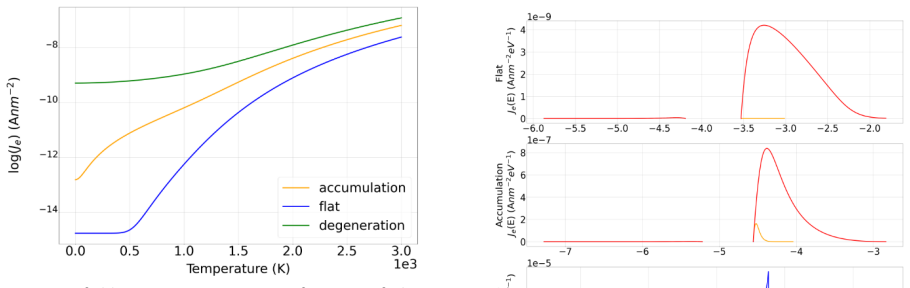
The central result is a corrected expression for the valence-band contribution to thermal-field emission, Eq. (15): $j_V = L \int_{-\infty}^{E_V} l_{FD}(E)\left(D(E) - \bar{\alpha} D(\bar{\alpha} E - \alpha E_V)\right) dE$, where $\alpha = m^*/m$, $\bar{\alpha} = 1 + m^*/m$, $L = qm/(2\pi^2\hbar^3)$, and $D$ is the JWKB-Kemble transmission coefficient. This differs from Stratton's Eq. (A1) by the absence of an additional term, $\ln\left\{1 + e^{E_V/kT}\right\}$ times an integral of $D$ over the valence-band edge, which the authors show arises from an incorrect partial integration in the original derivation. They also report that a fourth-order polynomial fit to the Gamow function $G(E_n; F, R, \gamma)$ reproduces the full JWKB current density and Nottingham heat with RMSE $0.01531$ and $0.02987$ respectively, at roughly sixfold speedup. With this tool, they find that the emitted electron energy distribution transitions from metal-like to conduction-band-dominated to valence-band-dominated as the field decreases, and that a measurable crossover between conduction and valence contributions could reveal the semiconductor band gap.
Load-bearing premise
The predictions stand on the assumption that the three imposed band-bending scenarios (flat band, $E_C = E_F$, $E_C \ll E_F$) correctly represent how a real semiconductor's bands respond to the applied field, and that mapping is never derived or validated.
Editorial extensions
If this is right
- At cryogenic temperatures, the corrected equation changes the predicted magnitude of valence-band emission, which may explain why valence-band electrons have not been observed in experiments and points to the conditions under which they should be.
- The conduction and valence contributions cross at a specific applied field; at that crossover, the model predicts the band gap should become visible in the emitted electron energy distribution.
- The model predicts that n-type semiconductor emitters also exhibit current saturation at high fields once the surface degenerates, extending a saturation effect that has been observed experimentally in p-type materials.
- Because the polynomial-fit approach reproduces full JWKB results across all emission regimes, the same speedup strategy is applicable to photo-emission and to emitters with more complex supply functions.
Reading between the lines
- If the removal of the logarithmic term is correct, published analyses of cryogenic semiconductor emission that used Stratton's original expression may need to be revisited, and the discrepancy might show up most strongly in Nottingham heating at low temperature.
- The paper's imposed band-bending scenarios are a necessary simplification; the natural next step is to couple GETELEC-2.0 with self-consistent Poisson-continuity-heat loops and check whether the predicted saturation and crossover points move, since the field-to-bending mapping is currently assumed.
- The polynomial-fitting strategy for $G(E_n)$ could be exported to any emission model where the barrier is a smooth function of a few parameters, making full JWKB accuracy affordable in large 3D emitter simulations.
- The dynamic-range explanation for missing valence-band spectra is testable: run a high-dynamic-range electron energy analyzer at the predicted conduction/valence crossover field and look for the two-peak plus band-gap structure.
Editorial analysis
A structured set of objections, weighed in public.
Referee Report
Summary. The paper reviews Stratton's thermal-field emission theory for semiconductors, claims to correct the valence-band emission equation, and presents GETELEC-2.0, an extension of an existing numerical emission code. The new code evaluates conduction- and valence-band emission integrals, Nottingham heat, and electron energy distributions using a precomputed fourth-order polynomial fit to the JWKB Gamow function. The authors validate this interpolation against full numerical integration, simulate intrinsic Ge under three imposed band-bending scenarios, and discuss field, temperature, and Nottingham-heat dependences. The central theoretical claim is that Eq. (15) removes an erroneous logarithmic boundary term from Stratton's valence-band formula, which they argue explains the scarcity of observed valence-band emission and predicts valence-band-dominated emission at cryogenic temperatures.
Significance. If the corrected valence-band integral is rigorously established, the paper would provide a useful correction to a long-standing formula and a practical computational tool for semiconductor field-emission simulation, including energy distributions and Nottingham heating. The numerical strategy of tabulating polynomial fits to the Gamow function is transparent and is validated over a broad parameter range (RMSE 0.01531 for current density and 0.02987 for Nottingham heat), and the authors explicitly acknowledge the main physical limitations: the deferred self-consistent band-bending calculation, the assumed replacement-electron energy, and the neglect of surface states. However, the headline theoretical derivation currently contains an algebraic sign error in the supply function that, as written, makes the central valence-band result false at cryogenic temperatures, so the significance cannot be assessed until the derivation and all subsequent figures are corrected.
major comments (3)
- [Section II.B, Eq. (11); Appendix Eqs. (A.25), (A.55)] The supply function is defined with the wrong sign. Eq. (11) gives lFD(E) = ln(1 + e^((E-Ef)/kT)), whose derivative is lFD'(E) = (1/kT)(1 - fFD(E)). Therefore the identity used in Eqs. (A.25) and (A.55), namely that the emitted-current integrand can be written as -lFD'(E) g(E), is algebraically false: -lFD'(E) = -(1/kT)(1 - fFD(E)), not fFD(E). The function whose derivative is -fFD(E) is ln(1 + e^((Ef-E)/kT)), i.e., the standard supply function with the opposite sign in the exponent. With the printed definition, Eq. (15) gives essentially zero valence-band current at low temperature for E below EV, directly contradicting the paper's claim that valence-band emission dominates at cryogenic temperatures. In addition, the integration by parts in Eq. (A.27) and Eq. (A.57) is missing the kT prefactor that must appear when the derivative of a dimensionless log-supply function is used. The sign convention and the kT factor must be corrected, and the derivation of Eq. (15) must be redone, before the claimed correction of Stratton's valence-band equation can be accepted.
- [Appendix A.2, Eqs. (A.38) and (A.45)] The valence-band change of variables is internally inconsistent. Eq. (A.38) does not follow from Eqs. (A.33)-(A.36): substituting Ebar = Ev - epsilon and epsilon = EV - E into DV(Ebar + Ebar_r) gives a different argument than the printed DV(EV - E + pr^2/2m). Eq. (A.45) also has the wrong sign on the pz^2 term: from E = EV - (pz^2 + pr^2)/(2m*) one obtains E = EV - pz^2/(2m*) - (m/m*)Er, not E = EV - (m/m*)Er + pz^2/(2m*). Although the resulting integration limit in Eq. (A.46) may survive this particular sign error, the derivation as a whole is not reproducible. These errors are load-bearing because Eq. (15) is obtained from this chain of substitutions, and the claimed boundary-term difference between Eq. (A.60) and Stratton's Eq. (A.61) cannot be verified until the change of variables, the Jacobian orientation, and the integration-by-parts boundary term are all corrected.
- [Section IV, Figs. 6 and 8] The field-dependent predictions are computed from imposed band-bending scenarios, not from a self-consistent solution. Section II.A explicitly defers the Poisson-continuity-heat self-consistent loops to a forthcoming publication, and Section IV states that all results use the zero-current approximation with pre-set band positions. Consequently, the saturation in Fig. 6, the conduction/valence crossover, and the temperature dependence in Fig. 8 are predictive only under an assumed, unvalidated mapping between the applied field and the band displacement (EC-EF). A different, physically correct mapping could change the crossover point and the saturation behavior even if the emission integrals were exact. The authors acknowledge this limitation in the conclusions, but the manuscript's abstract and Section IV present these results as explanations of experimental observations. The claims should be reframed as illustrative calculations for prescribed band geometries, or the model should be coupled to at least a simplified self-consistent band-bending calculation and the mapping validated.
minor comments (6)
- [Abstract and Section IV.1] The abstract contains the typo 'Key works' instead of 'Key words', and in Section IV.1 the sentence 'it has such a low magnitude in comparison with that of the emission from the valence band' should read 'conduction band'.
- [Eq. (5)] The symbol Q in the barrier expression is never defined; if it denotes the image-potential coefficient, it should be written explicitly (e.g., Q = q^2/(16*pi*epsilon_0)) so that the barrier model is self-contained.
- [Eq. (20)] The expression U(z) = F R(gamma-1)z + z^2/(gamma z + R(gamma-1)) is ambiguous as typeset; parentheses should be added to make the denominator unambiguous, and the parameters should be related to Eq. (5).
- [Figure numbering] A figure caption is duplicated: the caption 'Figure 2: Evolution of the Nottingham heat' refers to a later figure, not the schematic in Section II.A; renumber the figures.
- [Section IV.1] The effective masses are quoted as 'm*e = 0.98m kg and m*h = 0.59m kg'; this should be written as m*e = 0.98 m_0 and m*h = 0.59 m_0, where m_0 is the free-electron mass, to avoid dimensional confusion.
- [Section III] The text refers to Eqs. (21-22) and Eq. (23) for the barrier approximation and asymptotic forms, but these equations are not all displayed or clearly numbered in the manuscript; please check the equation numbering and display all referenced expressions.
Circularity Check
No significant circularity: the emission integrals, polynomial interpolation, and band-scenario results are derived from stated Stratton/JWKB inputs and internal numerical consistency, not from the quantities they predict.
full rationale
The paper's central theoretical claim is Eq. (15), obtained from Eq. (14) by explicit coordinate changes (Appendix Eqs. A.42-A.60) and integration by parts; the inputs (Fermi-Dirac distribution, transmission coefficient, band edges, effective masses) are not defined in terms of the predicted current. The claimed correction relative to Stratton is a mathematical manipulation of the same supply and transmission functions, not a fit. The polynomial coefficients in Section III are an interpolation of the model's own numerically integrated Gamow function G(En; F, R, gamma), and validation compares GETELEC-2.0 against the full JWKB integration (Fig. 3, RMSE = 0.01531 and 0.02987); this is an internal numerical approximation with error metrics, not a fitted physical parameter renamed as a prediction. Band-bending scenarios are imposed inputs, not outputs of the model, and the paper explicitly defers self-consistent loops to a forthcoming publication; any unvalidated mapping from applied field to band bending is a correctness or assumption issue, not circularity. Self-citations to GETELEC 1.0 and the Kyritsakis barrier expansion are load-bearing only as published computational and mathematical tools with stated assumptions and independent derivations, while the semiconductor emission equations rest on Stratton and Kemble/JWKB, not on an unverified self-citation chain. No step reduces by construction to its own input, so the circularity score is 0.
Assumptions & free parameters
assumptions (7)
- standard math JWKB/Kemble transmission formula D(E_n)=1/(1+e^{G(E_n)}) with Gamow integral (Eqs. 3-4).
- domain assumption Quasi-planar emitter approximation: the tunneling barrier is one-dimensional and tangential field dependence is ignored (Section II.B).
- domain assumption Effective-mass approximation with free-electron mass in the transverse kinetic energy, conserving transverse crystal momentum (Eqs. 6-7).
- domain assumption Band positions (flat band, EC=EF, EC<<EF) are prescribed inputs under the zero-current approximation; Poisson, continuity, and heat equations are not solved (Fig. 2 loops deferred).
- domain assumption Replacement electron energy for Nottingham heat is set equal to EF (Section III, Conclusions).
- domain assumption Emitter surface is smooth and free of surface states (Conclusions limitation).
- domain assumption The vacuum barrier shape is approximated by the empirical formula Eq. (20) with asymptotic behavior from Refs. [17] and [18], rather than computed exactly.
Cite this review
Pith. "Pith review of Theory and computation of thermal-field emission from semiconductors." pith.science (2026). https://pith.science/paper/XNRAMY6F
@misc{pith2026250606198,
  author       = {Pith},
  title        = {Pith review of: Theory and computation of thermal-field emission from semiconductors},
  year         = {2026},
  howpublished = {\url{https://pith.science/paper/XNRAMY6F}},
  note         = {Machine review of arXiv:2506.06198}
}
read the original abstract
Semiconducting field emitters present some interesting features (e.g.; self-limited electron emission) for both scientific interest and industrial applications. The analysis of experimental results and device design has been restrained by the lack of accurate 3D models for the simulation of thermal-field emission from semiconductors. Here we review and correct the equations of field emission from semiconductors and include them to expand GETELEC (General Tool for Electron Emission Calculations). Our method covers all electron emission regime (field, thermal, and intermediate), aiming to maximise the calculation accuracy while minimising the computational cost. GETELEC-2.0 is able to reproduce the characteristic non-linear I-V curves in Fowler-Nordheim coordinates obtained from semiconductors, giving insights about their nature. As well as providing an explanation to the lack of experimental observation of valence band electrons from semiconductors.
Figures
Reference graph
Works this paper leans on
-
[1]
Current saturation in field emission from H -passivated Si nanowires,
M. Choueib, R. Martel, C. S. Cojocaru, A. Ayari, P. Vincent, and S. T. Purcell, “Current saturation in field emission from H -passivated Si nanowires,” ACS Nano, vol. 6, no. 8, pp. 7463 –7471, Aug. 2012, doi: 10.1021/nn302744e
-
[2]
Fursey, Field Emission in Vacuum Microelectronics
G. Fursey, Field Emission in Vacuum Microelectronics. 2003
2003
-
[3]
Field Emission Beyond Information Displays,
S. B. Cárceles, A. Kyritsakis, V. Zadin, A. Mavalankar, and I. Underwood, “Field Emission Beyond Information Displays,” i n Digest of Technical Papers - SID International Symposium, John Wiley and Sons Inc, 2023, pp. 366 –369. doi: 10.1002/sdtp.16568
-
[4]
M. E. Swanwick, P. D. Keathley, F. X. Kartner, and L. F. Velasquez-Garcia, “Ultrafast photo -triggered field emission cathod es using massive, uniform arrays of nano -sharp high- aspect-ratio silicon structures,” 2013 Transducers and Eurosensors XXVII: The 17th International Conference on Solid -State Sensors, Actuators and Microsystems, TRANSDUCERS and E...
-
[5]
Addressable flat-panel x- ray sources for medical, security, and industrial applications,
G. Travish, F. J. Rangel, M. A. Evans, K. Schmiedehausen, and B. Hollister, “Addressable flat-panel x- ray sources for medical, security, and industrial applications,” Peocedings of Spie , vol. 8502, no. October 2012, 2012, doi: 10.1117/12.929354
-
[6]
J. V. Sci et al. , “All field emission experiments are noisy , … are any meaningful ? All field emission experiments are noisy , … are any meaningful ?,” vol. 024001, no. November 2022, 2023, doi: 10.1116/6.0002338
-
[7]
A general computational method for electron emission and thermal effects in field emitting nanotips,
A. Kyritsakis and F. Djurabekova, “A general computational method for electron emission and thermal effects in field emitting nanotips,” Comput Mater Sci , vol. 128, no. 4, pp. 15 –21, Feb. 2017, doi: 10.1016/j.commatsci.2016.11.010
-
[8]
X. Gao et al. , “evaporation and critical electric field of copper Molecular dynamics simulations of thermal evaporation and critical electric field of copper nanotips,” 2020
work page 2020
Show all 26 references
-
[9]
Field emission from semiconductors,
R. Stratton, “Field emission from semiconductors,” Proceedings of the Physical Society. Section B , vol. 68, no. 10, pp. 746 –757, 1955, doi: 10.1088/0370-1301/68/10/307
1955 doi
-
[10]
Theory of Field Emission from Semiconductors,
R. Stratton, “Theory of Field Emission from Semiconductors,” Physical Review, vol. 125, no. 1, pp. 67–82, 1962, doi: 10.1103/PhysRev.125.67
1962 doi
-
[11]
General features of field emission from semiconductors,
L. M. Baskin, O. I. Lvov, and G. N. Fursey, “General features of field emission from semiconductors,” Physica Status Solidi (B), vol. 47, no. 1, pp. 49 –62, 1971, doi: 10.1002/pssb.2220470105
1971 doi
-
[12]
Modinos, Field, Thermionic, and Secondary Electron Emiss ion Spectroscopy, vol
A. Modinos, Field, Thermionic, and Secondary Electron Emiss ion Spectroscopy, vol. 102, no. 1. Boston, MA: Springer US, 1984. doi: 10.1007/978-1-4757-1448-7
1984 doi
-
[13]
Extension of the general thermal field equation for nanosized emitters,
A. Kyritsakis and J. P. Xanthakis, “Extension of the general thermal field equation for nanosized emitters,” J Appl Phys, vol. 119, no. 4, 2016, doi: 10.1063/1.4940721
2016 doi
-
[14]
Strong deviations from Fowler-Nordheim behavior for field emission from individual SiC nanowires due to restricted bulk carrier generation,
M. Choueib, A. Ayari, P. Vincent, M. Bechelany, D. Cornu, and S. T. Purcell, “Strong deviations from Fowler-Nordheim behavior for field emission from individual SiC nanowires due to restricted bulk carrier generation,” Phys Rev B Condens Matter Mater Phys , vol. 79, no. 7, Feb...
2009 doi
-
[15]
Energy distributions of field emitted electrons,
R. Stratton, “Energy distributions of field emitted electrons,” Physical Review, vol. 135, no. 3A, 1964, doi: 10.1103/PhysRev.135.A794
1964 doi
-
[16]
A Contribution to the Theory of the B. W. K. Method,
E. C. Kemble, “A Contribution to the Theory of the B. W. K. Method,” Physical Review, vol. 48, Sep. 1935, doi: 10.1103/PhysRev.48.549
1935 doi
-
[17]
Derivation of a generalized Fowler-Nordheim equation for nanoscopic field -emitters,
A. Kyritsakis and J. P. Xanthakis, “Derivation of a generalized Fowler-Nordheim equation for nanoscopic field -emitters,” Proceedings of the Roya l Society A: Mathematical, Physical and Engineering Sciences , vol. 471, no. 2174, 2015, doi: 10.1098/rspa.2014.0811
2015
-
[18]
General form of the tunneling barrier for nanometrically sharp electron emitters,
A. Kyritsakis, “General form of the tunneling barrier for nanometrically sharp electron emitters,” J Appl Phys, vol. 133, no. 11, Mar. 2023, doi: 10.1063/5.0144608
2023 doi
-
[19]
General formulation of thermal, field, and photoinduced electron emission,
K. L. Jensen, “General formulation of thermal, field, and photoinduced electron emission,” J Appl Phys, vol. 102, no. 2, 2007, doi: 10.1063/1.2752122
2007 doi
-
[20]
ENERGY DISTRIBUTION OF FIELD EMISSION FROM GERMAN IUM,
J. R. Arthur, “ENERGY DISTRIBUTION OF FIELD EMISSION FROM GERMAN IUM,” North - Holland Publishing Co, 1964
1964
-
[21]
S. M. Sze and K. K. Ng, Physics of semiconductor devices . Wiley - Interscience, 2007
2007
-
[22]
Energy exchange in field emission from semiconductors,
M. S. Chung, Y. J. Jang, A. Mayer, P. H. Cutler, N. M. Miskovsky, and B. L. Weis, “Energy exchange in field emission from semiconductors,” Journal of Vacuum Science & Technology B: Microelectronics and Nanometer Structures Processing, Measurement, and Phenomena , vol. 26, no. ...
2008 doi
-
[23]
Temperature - Dependent Field Emission and Breakdown Measurements Using a Pulsed High -Voltage Cryosystem,
M. Jacewicz, J. Eriksson, R. Ruber, S. Calatroni, I. Profatilova, and W. Wuensch, “Temperature - Dependent Field Emission and Breakdown Measurements Using a Pulsed High -Voltage Cryosystem,” Phys Rev Appl , vol. 14, no. 6, Dec. 2020, doi: 10.1103/PhysRevApplied.14.06100 2. APP...
2020 doi
-
[24]
1) where E = p2 2m∗ (𝐴
Emission equations for conduction band electrons jC = q 4π3ℏ3 ∫ fFD(E)D(E − Er) ∂E ∂pz d3p (𝐴. 1) where E = p2 2m∗ (𝐴. 2) Er = px 2 + py 2 2m = pr 2 2m (𝐴. 3) where m is the free electron mass of the electron m* is the effective mass of the electron We first change to polar co...
-
[25]
32) where E̅ = Ev − ε (𝐴
Emission Equations for valence band equations jV = q 4π3ℏ3 ∫ fFD(E̅)DV(E̅ + E̅r) ∂E̅ ∂pz d3p (𝐴. 32) where E̅ = Ev − ε (𝐴. 33) ε = EV − E = EV − p2 2m∗ = EV − pr 2 + pz 2 2m∗ (𝐴. 34) pr 2 = px 2 + py 2 (𝐴. 35) E̅r = pr 2 2m (𝐴. 36) and with DV(E) = D(EV − E) (𝐴. 37) we get DV(...
-
[26]
JV = fFD(E) ∫ D(Ez)dEz E α̅E−αEV (𝐴
From the later development, we can obtain the energy distribution of the electrons coming from the conduction band. JV = fFD(E) ∫ D(Ez)dEz E α̅E−αEV (𝐴. 62)
Reviewed August 7, 2026 · model on record in the stance chip above.
Discussion (0). Continue with ORCID to comment.