Optical control of conductivity type and valley polarization via persistent photoconductivity in (Pb,Sn)Se quantum wells
Pith reviewed 2026-05-20 07:53 UTC · model grok-4.3
The pith
Persistent photoconductivity converts (Pb,Sn)Se quantum wells from a threefold-degenerate M-valley hole gas to a single Gamma-valley electron gas while preserving mobility.
A machine-rendered reading of the paper's core claim, the machinery that carries it, and where it could break.
Core claim
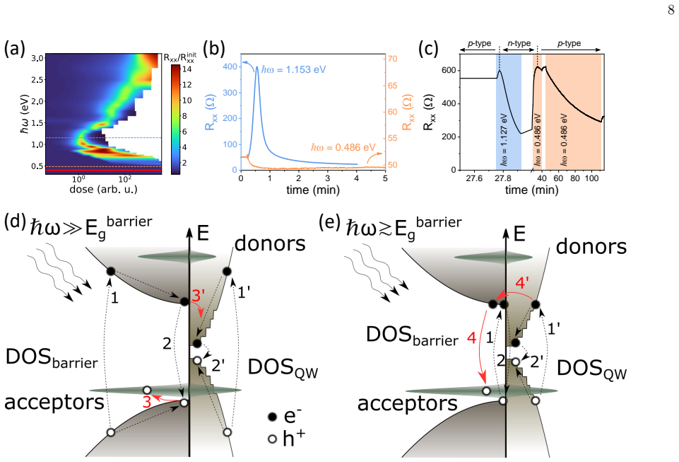
Illumination of these samples induces Fermi level shifts that convert the system from a threefold-degenerate M-valley two-dimensional hole gas to a single Gamma-valley-polarized electron gas with similar values of mobility. The optically induced state persists for more than 10^3 minutes at cryogenic temperatures and enables stepwise optical gating without the need for device processing. These transitions are confirmed by the sign inversion of the Hall slope and the modification of quantum Hall plateau degeneracies measured in magnetic fields up to 35 T. Landau level k·p model calculations quantitatively reproduce the experimental data.
What carries the argument
Persistent photoconductivity produced by donor and acceptor defect states in the (Pb,Eu)Se barrier that drive an upward Fermi-level shift inside the (Pb,Sn)Se well
If this is right
- The Hall slope reverses sign, indicating a change from hole to electron conduction.
- Quantum Hall plateau degeneracies change from threefold to non-degenerate, matching the valley switch.
- Electron mobility remains comparable to the original hole mobility.
- Appropriate photon energies can reverse the persistent photoconductivity and restore the original state.
- Weak-field magnetoresistance shows quantum localization effects at the boundary between weakly and strongly localized regimes.
Where Pith is reading between the lines
- The same defect-driven optical gating may apply to other IV-VI narrow-gap quantum wells for similar carrier-type control.
- The long persistence at cryogenic temperatures could support optically written, non-volatile valley states in reconfigurable devices.
- Identifying analogous defect configurations in different barrier materials would be required to extend the effect beyond cryogenic conditions.
Load-bearing premise
The persistent upward Fermi-level shift is produced by the specific energy positions of donor and acceptor defect states in the barrier material.
What would settle it
Direct spectroscopy of the barrier defect levels that places them at energies unable to trap holes while supplying electrons to the well would eliminate the proposed explanation for the observed persistent Fermi-level rise.
Figures


read the original abstract
The ability to tune the Fermi level of semiconductors is at the heart of modern electronics. Here, we demonstrate that persistent photoconductivity (PPC) enables tuning of carrier density, conductivity type, and, consequently, the valley polarization in (Pb,Sn)Se/(Pb,Eu)Se quantum wells. Illumination of these samples induces Fermi level shifts that convert the system from a threefold-degenerate $\bar{M}$-valley two-dimensional hole gas to a single $\bar{\Gamma}$-valley-polarized electron gas with similar values of mobility. The optically induced state persists for more than $10^{3}$ minutes at cryogenic temperatures and enables stepwise optical gating without the need for device processing. These transitions are confirmed by the sign inversion of the Hall slope and the modification of quantum Hall plateau degeneracies measured in magnetic fields up to 35 T. Landau level $k\cdot p$ model calculations quantitatively reproduce the experimental data. Furthermore, studies of weak-field magnetoresistance demonstrate the significance of quantum localization phenomena at the transition between the weakly and strongly localized regimes in compensated narrow-gap semiconductors. Spectral studies allow us to identify the critical role of the barrier material and determine the photon energies that can reverse the PPC effect. The persistent light-induced upward shift of the Fermi level in the $p$-type quantum well is explained in terms of specific energy positions of donor and acceptor defect states in the studied system. Our results demonstrate that PPC is a powerful optical gating tool for the IV-VI quantum wells, a versatile platform for reconfigurable valleytronic architectures.
Editorial analysis
A structured set of objections, weighed in public.
Referee Report
Summary. The manuscript demonstrates persistent photoconductivity (PPC) in (Pb,Sn)Se/(Pb,Eu)Se quantum wells as a means for optical control of carrier density, conductivity type, and valley polarization. Illumination converts a threefold-degenerate M-valley 2D hole gas into a single Gamma-valley electron gas with comparable mobility; the induced state persists >10^3 min at cryogenic temperatures. The transitions are evidenced by Hall slope sign inversion, altered quantum Hall plateau degeneracies up to 35 T, and quantitative agreement with k·p Landau level calculations. Spectral studies identify the barrier material's role, and the upward Fermi-level shift is attributed to specific donor/acceptor defect states.
Significance. If substantiated, the work provides a non-lithographic optical gating route for reconfigurable valleytronics in narrow-gap IV-VI quantum wells. The long-term persistence, direct transport signatures of valley reconfiguration, and matching model calculations constitute clear strengths. The additional observation of quantum localization at the weak-to-strong localization crossover in compensated narrow-gap systems is of independent interest.
major comments (2)
- [PPC mechanism discussion] Explanation of PPC mechanism (final paragraph of abstract and corresponding discussion section): The upward Fermi-level shift is ascribed to specific energy positions of donor and acceptor defect states in the barrier, yet no numerical defect energies, no comparison against the ~100 meV scale required for the M-to-Gamma valley switch, and no rate-equation or capture-cross-section estimate for the >10^3 min persistence are supplied. This quantitative gap is load-bearing for the claim that barrier-defect ionization produces the observed rigid carrier-type and valley reconfiguration.
- [Results on Hall and QH data] Transport data presentation (results section describing Hall and magnetoresistance measurements): While sign inversion of the Hall slope and changes in QH degeneracies are reported, the manuscript does not provide raw traces, error bars on extracted densities/mobilities, or explicit criteria for data selection across illumination cycles. These details are necessary to confirm that the claimed p-to-n conversion and degeneracy reduction are not affected by post-hoc fitting choices.
minor comments (2)
- Notation for valleys: The manuscript alternates between M and bar{M} (and Gamma and bar{Gamma}); a single consistent convention should be adopted throughout.
- Figure clarity: Magnetoresistance and Hall traces at successive illumination stages would benefit from explicit labeling of the illumination dose or photon energy on each curve.
Simulated Author's Rebuttal
We thank the referee for the careful and constructive review of our manuscript. We address each of the major comments in detail below and have prepared revisions to improve the clarity and quantitative support of the work.
read point-by-point responses
-
Referee: [PPC mechanism discussion] Explanation of PPC mechanism (final paragraph of abstract and corresponding discussion section): The upward Fermi-level shift is ascribed to specific energy positions of donor and acceptor defect states in the barrier, yet no numerical defect energies, no comparison against the ~100 meV scale required for the M-to-Gamma valley switch, and no rate-equation or capture-cross-section estimate for the >10^3 min persistence are supplied. This quantitative gap is load-bearing for the claim that barrier-defect ionization produces the observed rigid carrier-type and valley reconfiguration.
Authors: We agree that a more quantitative treatment of the defect energies and persistence mechanism would strengthen the discussion. The spectral dependence of the PPC effect, which activates only for photon energies exceeding the (Pb,Eu)Se barrier gap, directly constrains the relevant defect positions to lie within the barrier bandgap. This places the donor/acceptor levels at an energy scale sufficient to produce the observed upward Fermi-level shift of order 100 meV, matching the M-to-Gamma valley separation obtained from our k·p Landau-level calculations. The long persistence time at cryogenic temperatures is characteristic of deep traps with small capture cross-sections in narrow-gap IV-VI materials. In the revised manuscript we will add a dedicated paragraph (and a short supplementary note) that cites literature values for defect energies in PbEuSe (~150–250 meV below the conduction-band edge) and presents a simple rate-equation estimate using typical capture cross-sections of 10^{-19}–10^{-20} cm² to illustrate the expected lifetime. revision: partial
-
Referee: [Results on Hall and QH data] Transport data presentation (results section describing Hall and magnetoresistance measurements): While sign inversion of the Hall slope and changes in QH degeneracies are reported, the manuscript does not provide raw traces, error bars on extracted densities/mobilities, or explicit criteria for data selection across illumination cycles. These details are necessary to confirm that the claimed p-to-n conversion and degeneracy reduction are not affected by post-hoc fitting choices.
Authors: We thank the referee for highlighting the need for greater transparency. The raw Hall-resistance and magnetoresistance traces for successive illumination cycles are already contained in the Supplementary Information (Figs. S1–S3). In the revised main text we will add explicit cross-references to these figures and include error bars on all extracted carrier densities and mobilities, obtained from the standard deviation of repeated measurements under identical conditions. We have also inserted a concise description of the data-selection protocol: only traces acquired with fixed illumination power and duration, and with base temperature stable to within 0.1 K, were retained; no post-selection based on the sign of the Hall slope or the appearance of quantum-Hall plateaus was performed. revision: yes
Circularity Check
No significant circularity; central claims rest on direct experimental transport data.
full rationale
The paper's derivation chain begins with experimental Hall resistivity and magnetotransport measurements up to 35 T that directly exhibit Hall slope sign inversion and altered quantum Hall plateau degeneracies. These observations are interpreted as evidence for the p-to-n conversion and M-to-Gamma valley switch. The k·p Landau level calculations are invoked only to reproduce the measured traces after parameter adjustment, which is standard fitting rather than a first-principles prediction that loops back to the inputs. The PPC mechanism is attributed to donor/acceptor defect states in the barrier, but this remains a qualitative interpretive framework whose specific energies are not used to derive or force the transport signatures. No self-definitional equations, fitted quantities renamed as predictions, or load-bearing self-citations appear in the provided text. The result is therefore self-contained through independent empirical observations and conventional modeling.
Axiom & Free-Parameter Ledger
Lean theorems connected to this paper
-
IndisputableMonolith/Cost/FunctionalEquation.leanwashburn_uniqueness_aczel unclear?
unclearRelation between the paper passage and the cited Recognition theorem.
The persistent light-induced upward shift of the Fermi level in the p-type quantum well is explained in terms of specific energy positions of donor and acceptor defect states in the studied system.
What do these tags mean?
- matches
- The paper's claim is directly supported by a theorem in the formal canon.
- supports
- The theorem supports part of the paper's argument, but the paper may add assumptions or extra steps.
- extends
- The paper goes beyond the formal theorem; the theorem is a base layer rather than the whole result.
- uses
- The paper appears to rely on the theorem as machinery.
- contradicts
- The paper's claim conflicts with a theorem or certificate in the canon.
- unclear
- Pith found a possible connection, but the passage is too broad, indirect, or ambiguous to say the theorem truly supports the claim.
Reference graph
Works this paper leans on
-
[1]
and indicative of significant spin-orbit coupling in the system [58]. In MR data, this feature is most pro- nounced near the CNP, where a sharp W AL cusp appears around magnetic fields on the order of 10 mT. As the field increases above 100 mT, the positive MR is grad- ually replaced by a negative contribution, indicative of WL. Away from the CNP, both W ...
work page 2021
-
[2]
B. A. Bernevig, T. L. Hughes, and S.-C. Zhang, Quantum spin Hall effect and topological phase transition in HgTe quantum wells, Science314, 1757 (2006)
work page 2006
-
[3]
M. K¨ onig, S. Wiedmann, C. Br¨ une, A. Roth, H. Buh- mann, L. W. Molenkamp, X.-L. Qi, and S.-C. Zhang, Quantum spin Hall insulator state in HgTe quantum wells, Science318, 766 (2007)
work page 2007
-
[4]
R. Yu, W. Zhang, H.-J. Zhang, S.-C. Zhang, X. Dai, and Z. Fang, Quantized anomalous Hall effect in magnetic topological insulators, Science329, 61 (2010)
work page 2010
-
[5]
C.-Z. Chang, J. Zhang, X. Feng, J. Shen, Z. Zhang, M. Guo, K. Li, Y. Ou, P. Wei, L.-L. Wang, Z.-Q. Ji, Y. Feng, S. Ji, X. Chen, J. Jia, X. Dai, Z. Fang, S.-C. Zhang, K. He, Y. Wang, L. Lu, X.-C. Ma, and Q.-K. Xue, Experimental observation of the quantum anoma- lous Hall effect in a magnetic topological insulator, Sci- ence340, 167 (2013). 10
work page 2013
-
[6]
M. K. Sheinkman and A. Y. Shik, Long-term relaxation and residual conductivity of semiconductors, Sov. Phys. Semicond.10, 128 (1976)
work page 1976
-
[7]
A. Sumanth, K. Lakshmi Ganapathi, M. S. Ramachan- dra Rao, and T. Dixit, A review on realizing the mod- ern optoelectronic applications through persistent photo- conductivity, Journal of Physics D: Applied Physics55, 393001 (2022)
work page 2022
-
[8]
N. G. Semaltianos, G. Karczewski, B. Hu, T. Wojtow- icz, and J. K. Furdyna, Deep-level defects responsible for persistent photoconductivity in Ga-doped Cd 1−xMnxTe, Physical Review B51, 17499 (1995)
work page 1995
-
[9]
B. A. Akimov, V. A. Bogoyavlenskiy, L. I. Ryabova, and V. N. Vasil’kov, Experimental study of negative photo- conductivity inn-PbTe(Ga) epitaxial films, Physical Re- view B61, 16045 (2000)
work page 2000
- [10]
-
[11]
K. Bola˜ nos, S. de Castro, P. Rappl, E. Abramof, and M. Peres, Light-induced Shubnikov-de Haas oscillations and evidence of Dirac fermions inn-type PbTe single quantum well, Physica E: Low-dimensional Systems and Nanostructures144, 115458 (2022)
work page 2022
-
[12]
M. K. Sotnichuk, A. V. Ikonnikov, D. R. Khokhlov, N. N. Mikhailov, S. A. Dvoretsky, and V. I. Gavrilenko, Fea- tures of persistent photoconductivity in CdHgTe-based single quantum well heterostructures, Journal of Semi- conductors46, 042702 (2025)
work page 2025
-
[13]
A. Di Bartolomeo, L. Genovese, T. Foller, F. Giu- bileo, G. Luongo, L. Croin, S.-J. Liang, L. K. Ang, and M. Schleberger, Electrical transport and persistent photoconductivity in monolayer MoS 2 phototransistors, Nanotechnology28, 214002 (2017)
work page 2017
-
[14]
A. Grillo, E. Faella, A. Pelella, F. Giubileo, L. Ansari, F. Gity, P. K. Hurley, N. McEvoy, and A. Di Bartolomeo, Coexistence of negative and positive photoconductivity in few-layer PtSe 2 field- effect transistors, Advanced Functional Materials31, 10.1002/adfm.202105722 (2021)
-
[15]
A. L. Yeats, Y. Pan, A. Richardella, P. J. Mintun, N. Samarth, and D. D. Awschalom, Persistent optical gating of a topological insulator, Science Advances1, 10.1126/sciadv.1500640 (2015)
-
[16]
I. Nikolaev, A. Kazakov, K. Drozdov, M. Bannikov, K. Spirin, R. Menshchikov, S. Dvoretsky, N. Mikhailov, D. Khokhlov, and A. Ikonnikov, Bipolar persistent photo- conductivity in HgTe/CdHgTe double quantum well het- erostructures and its application for reversible change in the conductivity type, Journal of Applied Physics132, 234301 (2022)
work page 2022
-
[17]
M. Samani, A. V. Rossokhaty, E. Sajadi, S. L¨ uscher, J. A. Folk, J. D. Watson, G. C. Gardner, and M. J. Manfra, Low-temperature illumination and annealing of ultrahigh quality quantum wells, Physical Review B90, 10.1103/physrevb.90.121405 (2014)
-
[18]
A. Kazakov, G. Simion, Y. Lyanda-Geller, V. Kolkovsky, Z. Adamus, G. Karczewski, T. Wojtowicz, and L. P. Rokhinson, Mesoscopic transport in electrostatically de- fined spin-full channels in quantum Hall ferromagnets, Physical Review Letters119, 046803 (2017)
work page 2017
-
[19]
S. Wu, V. Fatemi, Q. D. Gibson, K. Watanabe, T. Taniguchi, R. J. Cava, and P. Jarillo-Herrero, Obser- vation of the quantum spin Hall effect up to 100 kelvin in a monolayer crystal, Science359, 76 (2018)
work page 2018
-
[20]
Fu, Topological crystalline insulators, Physical Review Letters106, 106802 (2011)
L. Fu, Topological crystalline insulators, Physical Review Letters106, 106802 (2011)
work page 2011
-
[21]
T. H. Hsieh, H. Lin, J. Liu, W. Duan, A. Bansil, and L. Fu, Topological crystalline insulators in the SnTe ma- terial class, Nature Communications3, 982 (2012)
work page 2012
- [22]
- [23]
-
[24]
S.-Y. Xu, C. Liu, N. Alidoust, M. Neupane, D. Qian, I. Belopolski, J. Denlinger, Y. Wang, H. Lin, L. Wray, G. Landolt, B. Slomski, J. Dil, A. Marcinkova, E. Mo- rosan, Q. Gibson, R. Sankar, F. Chou, R. Cava, A. Bansil, and M. Hasan, Observation of a topolog- ical crystalline insulator phase and topological phase transition in Pb 1−xSnxTe, Nature Communica...
-
[25]
J. Liu, W. Duan, and L. Fu, Two types of surface states in topological crystalline insulators, Physical Review B 88, 241303(R) (2013)
work page 2013
- [26]
- [27]
-
[28]
Springholz, Molecular beam epitaxy of IV-VI semiconductors, in Molecular Beam Epitaxy, edited by M
G. Springholz, Molecular beam epitaxy of IV-VI semiconductors, in Molecular Beam Epitaxy, edited by M. Henini (Elsevier, 2013) pp. 263–310
work page 2013
- [29]
-
[30]
G. Krizman, B. A. Assaf, T. Phuphachong, G. Bauer, G. Springholz, G. Bastard, R. Ferreira, L. A. de Vaulchier, and Y. Guldner, Tunable Dirac interface states in topological superlattices, Physical Review B98, 075303 (2018)
work page 2018
-
[31]
S. Yuan, G. Springholz, G. Bauer, and M. Kriechbaum, Electronic and optical properties of PbTe/Pb 1−xEuxTe multiple-quantum-well structures, Physical Review B49, 5476 (1994)
work page 1994
-
[32]
G. Krizman, J. Bermejo-Ortiz, T. Zakusylo, M. Ha- jlaoui, T. Takashiro, M. Rosmus, N. Olszowska, J. J. Ko/suppress lodziej, G. Bauer, Y. Guldner, G. Springholz, and L.- A. de Vaulchier, Valley-polarized quantum Hall phase in a strain-controlled Dirac system, Physical Review Letters 132, 166601 (2024)
work page 2024
-
[33]
G. Nimtz and B. Schlicht, Narrow-gap lead salts, in Narrow-Gap Semiconductors, Springer Tracts in Modern Physics, Vol. 98 (Springer Berlin Heidelberg, 1983) pp. 1–117
work page 1983
-
[34]
A. Kazakov, V. V. Volobuev, C.-W. Cho, B. A. Piot, Z. Adamus, T. Wojciechowski, T. Wojtowicz, G. Springholz, and T. Dietl, Topological phase diagram 11 and quantum magnetotransport effects in (Pb,Sn)Se quantum wells with magnetic barriers (Pb,Eu)Se, Phys- ical Review B111, 245419 (2025)
work page 2025
-
[35]
S. Majewski, M. Wierzbicki, and T. Dietl, From many valleys to many topological phases - quantum anoma- lous hall effect in IV-VI semiconductor quantum wells, arXiv:2601.16137 10.48550/ARXIV.2601.16137 (2026)
-
[36]
S. C. ten Kate, M. F. Ritter, A. Fuhrer, J. Jung, S. G. Schellingerhout, E. P. A. M. Bakkers, H. Riel, and F. Nichele, Small charging energies andg-factor anisotropy in PbTe quantum dots, Nano Letters22, 7049 (2022)
work page 2022
-
[37]
M. Gomanko, E. J. de Jong, Y. Jiang, S. G. Schellinger- hout, E. Bakkers, and S. Frolov, Spin and orbital spec- troscopy in the absence of coulomb blockade in lead tel- luride nanowire quantum dots, SciPost Physics13, 089 (2022)
work page 2022
-
[38]
S. G. Schellingerhout, R. Bergamaschini, M. A. Verhei- jen, F. Montalenti, L. Miglio, and E. P. Bakkers, In- plane nanowire growth of topological crystalline insu- lator Pb 1−xSnxTe, Advanced Functional Materials33, 2305542 (2023)
work page 2023
-
[39]
W. Song, Y. Wang, W. Miao, Z. Yu, Y. Gao, R. Li, S. Yang, F. Chen, Z. Geng, Z. Zhang, S. Zhang, Y. Zang, Z. Cao, D. E. Liu, R. Shang, X. Feng, L. Li, Q.-K. Xue, K. He, and H. Zhang, Conductance quantization in PbTe nanowires, Physical Review B108, 045426 (2023)
work page 2023
-
[40]
G. Hussain, K. Warda, G. Cuono, and C. Autieri, Density functional theory study of the spin-orbit insulating phase in snte cubic nanowires: Implications for topological elec- tronics, ACS Applied Nano Materials7, 8044 (2024)
work page 2024
- [41]
-
[42]
G. P. Mazur, K. Dybko, A. Szczerbakow, J. Z. Domagala, A. Kazakov, M. Zgirski, E. Lusakowska, S. Kret, J. Ko- rczak, T. Story, M. Sawicki, and T. Dietl, Experimental search for the origin of low-energy modes in topological materials, Physical Review B100, 041408(R) (2019)
work page 2019
-
[43]
W. Brzezicki, M. M. Wysoki´ nski, and T. Hyart, Topo- logical properties of multilayers and surface steps in the SnTe material class, Physical Review B100, 121107(R) (2019)
work page 2019
-
[44]
N. M. Nguyen, W. Brzezicki, and T. Hyart, Corner states, hinge states, and Majorana modes in SnTe nanowires, Physical Review B105, 075310 (2022)
work page 2022
-
[45]
G. Hussain, G. Cuono, P. Dziawa, D. Janaszko, J. Sad- owski, S. Kret, B. Kurowska, J. Polaczy´ nski, K. Warda, S. Sattar, C. M. Canali, A. Lau, W. Brzezicki, T. Story, and C. Autieri, Pentagonal nanowires from topological crystalline insulators: a platform for intrinsic core-shell nanowires and higher-order topology, Nanoscale Horizons 9, 1290 (2024)
work page 2024
-
[46]
A. Kawala and W. Brzezicki, Topological properties of the [110] SnTe nanowires, Physical Review B112, 035102 (2025)
work page 2025
-
[47]
R. Yoshimi, R. Kurihara, Y. Okamura, H. Handa, N. Ogawa, M. Kawamura, A. Tsukazaki, K. S. Taka- hashi, M. Kawasaki, Y. Takahashi, M. Tokunaga, and Y. Tokura, Emergence of ferroelectric topological insula- tor as verified by quantum Hall effect of surface states in (Sn,Pb,In)Te films, Physical Review Letters134, 176602 (2025)
work page 2025
-
[48]
G. Krizman, A. Kazakov, C.-W. Cho, V. V. Volobuev, A. Majou, E. B. Achour, T. Wojtowicz, G. Bauer, Y. Guldner, B. A. Piot, T. Jolicoeur, G. Springholz, and L.-A. de Vaulchier, Spontaneous breaking of the SU(3) flavor symmetry in a quantum Hall valley nematic, arXiv:2510.13874 10.48550/ARXIV.2510.13874 (2025)
-
[49]
F. S. Pena, M. L. Peres, M. J. P. Pirralho, D. A. W. Soares, C. I. Fornari, P. H. O. Rappl, and E. Abramof, Fast photoresponse and high parallel transport inn-type PbTe/PbEuTe quantum wells, Applied Physics Letters 111, 192105 (2017)
work page 2017
-
[50]
G. R. F. Lopes, S. de Castro, B. Kawata, P. H. d. O. Rappl, E. Abramof, and M. L. Peres, Photoconductiv- ity effect in SnTe quantum well, Applied Physics Letters 119, 10.1063/5.0056230 (2021)
- [51]
-
[52]
See Supplemental Material at [URL will be inserted by publisher] for barrier material characterization, addi- tional magnetotransport data for the sample B and ad- ditional datasets for samples A, C and D
-
[53]
Y. I. Ravich, B. A. Efimova, and V. I. Tamarchenko, Scattering of current carriers and transport phenomena in lead chalcogenides II. experiment, Physica Status So- lidi (b)43, 453 (1971)
work page 1971
- [54]
- [55]
-
[56]
Y. J. Chung, A. Gupta, K. W. Baldwin, K. W. West, M. Shayegan, and L. N. Pfeiffer, Understanding limits to mobility in ultrahigh-mobility GaAs two-dimensional electron systems: 100 million cm 2/Vs and beyond, Phys- ical Review B106, 075134 (2022)
work page 2022
- [57]
- [58]
-
[59]
B. Turowski, A. Kazakov, R. Rudniewski, T. Sobol, E. Partyka-Jankowska, T. Wojciechowski, M. Aleszkiewicz, W. Zaleszczyk, M. Szczepanik, T. Wo- jtowicz, and V. V. Volobuev, Spin-polarization of topological crystalline and normal insulator Pb 1−xSnxSe (111) epilayers probed by photoelectron spectroscopy, Applied Surface Science610, 155434 (2023)
work page 2023
-
[60]
M. O. Nestoklon and N. S. A verkiev, Nondiffusion the- ory of weak localization magnetoresistance in graphene, Physical Review B90, 155412 (2014)
work page 2014
-
[61]
A. Kazakov, W. Brzezicki, T. Hyart, B. Turowski, J. Polaczy´ nski, Z. Adamus, M. Aleszkiewicz, T. Woj- ciechowski, J. Z. Domagala, O. Caha, A. Varykhalov, G. Springholz, T. Wojtowicz, V. V. Volobuev, and T. Di- etl, Signatures of dephasing by mirror-symmetry break- 12 ing in weak-antilocalization magnetoresistance across the topological transition in Pb 1...
work page 2021
- [62]
- [63]
-
[64]
H. Pascher, G. Bauer, and R. Grisar, Magnetooptical in- vestigations and four-wave-mixing spectroscopy of PbSe, Physical Review B38, 3383 (1988)
work page 1988
-
[65]
A. Shuvaev, V. Dziom, J. Gospodariˇ c, E. G. Novik, A. A. Dobretsova, N. N. Mikhailov, Z. D. Kvon, and A. Pi- menov, Band structure near the Dirac point in HgTe quantum wells with critical thickness, Nanomaterials12, 2492 (2022)
work page 2022
-
[66]
M. Meyer, T. F¨ ahndrich, S. Schmid, A. Wolf, S. S. Krish- topenko, B. Jouault, G. Bastard, F. Teppe, F. Hartmann, and S. H¨ ofling, Coexistence of topological and normal insulating phases in electro-optically tuned InAs/GaSb bilayer quantum wells, Physical Review B109, l121303 (2024)
work page 2024
-
[67]
J. Hinz, H. Buhmann, M. Sch¨ afer, V. Hock, C. Becker, and L. Molenkamp, Gate control of the giant Rashba effect in HgTe quantum wells, Semiconductor Science and Technology21, 501 (2006)
work page 2006
-
[68]
L. Lunczer, P. Leubner, M. Endres, V. L. M¨ uller, C. Br¨ une, H. Buhmann, and L. W. Molenkamp, Ap- proaching quantization in macroscopic quantum spin Hall devices through gate training, Physical Review Let- ters123, 10.1103/physrevlett.123.047701 (2019)
-
[69]
P. M. Mooney, Deep donor levels (DXcenters) in III- V semiconductors, Journal of Applied Physics67, R1 (1990)
work page 1990
-
[70]
T. Wojtowicz, S. Kole´ snik, I. Miotkowski, and J. K. Fur- dyna, Magnetization of bound magnetic polarons: Direct determination via photomemory effect, Physical Review Letters70, 2317 (1993)
work page 1993
-
[71]
N. G. Semaltianos, G. Karczewski, T. Wojtowicz, and J. K. Furdyna, Persistent photoconductivity and photoionization of deep electron traps in Ga-doped Cd1−xMnxTe, Physical Review B47, 12540 (1993)
work page 1993
-
[72]
A. I. Belogorokhov, B. A. Volkov, I. I. Ivanchik, and D. R. Khokhlov, Model ofDX-like impurity centers in PbTe(Ga), Journal of Experimental and Theoretical Physics Letters72, 123 (2000)
work page 2000
- [73]
-
[74]
S. Lany and A. Zunger, Anion vacancies as a source of persistent photoconductivity in ii-vi and chalcopyrite semiconductors, Physical Review B72, 035215 (2005)
work page 2005
-
[75]
B. Kowalski, Z. Go/suppress lacki, E. Guziewicz, A. Kozanecki, B. Or/suppress lowski, J. Ghijsen, and R. Johnson, Rare earth 4f states in A IV 1−xRExBV I diluted magnetic semiconductors, Journal of Alloys and Compounds286, 121 (1999)
work page 1999
-
[76]
V. V. Volobuev, P. S. Mandal, M. Galicka, O. Caha, J. S´ anchez-Barriga, D. D. Sante, A. Varykhalov, A. Khiar, S. Picozzi, G. Bauer, P. Kacman, R. Buczko, O. Rader, and G. Springholz, Giant Rashba splitting in Pb1−xSnxTe (111) topological crystalline insulator films controlled by Bi doping in the bulk, Advanced Materials 29, 1604185 (2017)
work page 2017
-
[77]
J. R. Williams, L. DiCarlo, and C. M. Marcus, Quantum Hall effect in a gate-controlledp-njunction of graphene, Science317, 638 (2007)
work page 2007
-
[78]
D. A. Abanin and L. S. Levitov, Quantized transport in graphenep-njunctions in a magnetic field, Science317, 641 (2007)
work page 2007
-
[79]
C. Fang, M. J. Gilbert, and B. A. Bernevig, Large- Chern-number quantum anomalous Hall effect in thin- film topological crystalline insulators, Physical Review Letters112, 046801 (2014)
work page 2014
-
[80]
A. Kr´ olicka, K. Gas, W. Dobrowolski, H. Przybyli´ nska, Y. K. Edathumkandy, J. Korczak, E. /suppress Lusakowska, R. Minikayev, A. Reszka, R. Jakie/suppress la, L. Kowal- czyk, A. Mirowska, M. Gryglas-Borysiewicz, J. Kossut, M. Sawicki, A. /suppress Lusakowski, P. Bogus/suppress lawski, T. Story, and K. Dybko, Cr resonant impurity for studies of band inv...
work page 2025
discussion (0)
Sign in with ORCID, Apple, or X to comment. Anyone can read and Pith papers without signing in.