Post Annealing Crystallization behavior of RF Sputtered Yttrium Iron Garnet thin films on Si/SiO2 patterned substrates
Pith reviewed 2026-06-27 21:09 UTC · model grok-4.3
The pith
Patterned SiO2 buffer layers on silicon allow RF-sputtered YIG films to crystallize during furnace annealing, establishing a route to suspended magnonic devices.
A machine-rendered reading of the paper's core claim, the machinery that carries it, and where it could break.
Core claim
Depositing a 390 nm YIG film by low-vacuum RF sputtering onto 240 nm SiO2 on Si, then recrystallizing it in a horizontal furnace under O2 at 750-850 degrees Celsius, produces crystallized YIG when fluorine-etched hole pairs in the SiO2 serve as seed nucleation points, thereby establishing a fabrication route toward fully suspended and released YIG devices once compositional control is achieved.
What carries the argument
The fluorine-etched hole pairs patterned into the SiO2 buffer layer, which function as seed nucleation points that direct the crystallization of the overlying YIG film during post-deposition furnace annealing.
If this is right
- Suspended YIG structures can be released from the Si/SiO2 substrate after crystallization.
- Optimized stoichiometry would permit the crystallized films to be transferred onto alternative substrates.
- Magnonic devices relying on long-range magnon propagation become feasible with this deposition and annealing sequence.
- Patterned nucleation points enable control over where and how the YIG crystallizes on the buffer layer.
Where Pith is reading between the lines
- The same patterning-plus-annealing sequence could be tested on other garnet compositions to broaden the range of releasable magnetic films.
- If the crystallized YIG meets magnon requirements, the method could be combined with standard silicon release processes to create hybrid magnonic-photonic chips.
- Lower-vacuum sputtering plus furnace annealing might reduce equipment barriers for early-stage magnonic prototyping compared with fully in-situ high-vacuum growth.
Load-bearing premise
That low-vacuum RF sputtering followed by furnace annealing on the Si/SiO2 interface will yield YIG films with enough crystallinity, correct stoichiometry, and magnon propagation properties to function in devices.
What would settle it
X-ray diffraction patterns or compositional analysis showing persistent amorphous regions or large deviations from Y3Fe5O12 stoichiometry in the annealed films on patterned substrates would show the route does not produce usable crystallized YIG.
Figures
read the original abstract
Yttrium Iron Garnet YIG (Y3Fe5O12), is a commonly used material for magnonic devices due to its crystal and chemical structure, which makes the material highly ferromagnetic and enables long-range magnon propagation. Magnonic devices were fabricated by depositing a 390 nm thick thin film of YIG, using low vacuum RF sputtering, on Si substrates with a 240 nm buffer layer of SiO2. Two sets of devices were used to study the effect of the Si/SiO2 interface on the YIG. The first set features patterned hole pairs on the SiO2, which was created using fluorine etching. Patterned samples were used as seed nucleation points to study the crystallization behavior. The second set was a non-patterned Si/SiO2 with YIG deposited uniformly on the top. Post-deposition recrystallization of the YIG film was accomplished in a horizontal furnace under O2 atmosphere, between 750 degrees C and 850 degrees C. By patterning devices with a SiO2 buffer layer, depositing YIG via RF sputtering, and subsequently crystallizing the films in a furnace, we establish a fabrication route toward devices that can be suspended. Although further optimization of stoichiometry is required, achieving precise compositional control would enable the realization of fully suspended and released YIG devices that can be transferred onto alternative substrates.
Editorial analysis
A structured set of objections, weighed in public.
Referee Report
Summary. The manuscript describes deposition of 390 nm YIG films by low-vacuum RF sputtering onto Si substrates with a 240 nm SiO2 buffer layer, followed by furnace annealing in O2 at 750–850 °C. Patterned hole pairs etched into the SiO2 are used as nucleation sites; the authors state that this sequence establishes a fabrication route toward suspended magnonic devices, while noting that further stoichiometry optimization is still required.
Significance. If post-anneal films on both patterned and blanket regions were shown to form the correct garnet phase with near-ideal Y:Fe stoichiometry and low damping, the approach could enable transferrable suspended YIG structures. No such evidence is supplied, so the potential impact cannot be assessed from the present text.
major comments (1)
- [Abstract] Abstract: the assertion that the described process 'establishes a fabrication route toward devices that can be suspended' is unsupported. The text supplies no XRD, EDX, XPS, FMR linewidth, or any other quantitative metric confirming that the annealed films crystallize into phase-pure YIG with usable magnon-propagation properties.
Simulated Author's Rebuttal
We thank the referee for the detailed review and constructive comments on our manuscript. We address the major comment point by point below and agree that revisions to the abstract are needed to align the claims more closely with the presented results.
read point-by-point responses
-
Referee: [Abstract] Abstract: the assertion that the described process 'establishes a fabrication route toward devices that can be suspended' is unsupported. The text supplies no XRD, EDX, XPS, FMR linewidth, or any other quantitative metric confirming that the annealed films crystallize into phase-pure YIG with usable magnon-propagation properties.
Authors: We agree that the manuscript does not include quantitative metrics such as XRD, EDX, XPS, or FMR data to confirm phase-pure YIG formation or magnon properties. The work focuses on post-annealing crystallization behavior using patterned nucleation sites on Si/SiO2, with the explicit statement that further stoichiometry optimization is required. We will revise the abstract to describe the process as providing a potential fabrication route toward suspended devices, contingent on additional optimization and characterization, rather than claiming it establishes the route outright. revision: yes
Circularity Check
No circularity: purely descriptive experimental fabrication report
full rationale
The manuscript describes an experimental process (RF sputtering of YIG on patterned Si/SiO2, post-anneal crystallization) and states a fabrication route was established, while explicitly noting that stoichiometry optimization is still required. There are no equations, derivations, fitted parameters, predictions, or first-principles claims that could reduce to inputs by construction. No self-citations, ansatzes, or uniqueness theorems are invoked. The work contains no load-bearing logical chain that could exhibit circularity.
Axiom & Free-Parameter Ledger
Reference graph
Works this paper leans on
-
[1]
This is significant because the etching of a highly single- crystalline material defines the geometry of the device, low arXiv:2606.07886v1 [cond-mat.mtrl-sci] 5 Jun 2026 2 side wall roughness, and high design control, all of which affect magnon propagation. Secondly, highly stoichiomet- ric precursors are required to minimize impurities and scat- tering ...
Pith/arXiv arXiv 2026
-
[2]
(b) Between hole pairs
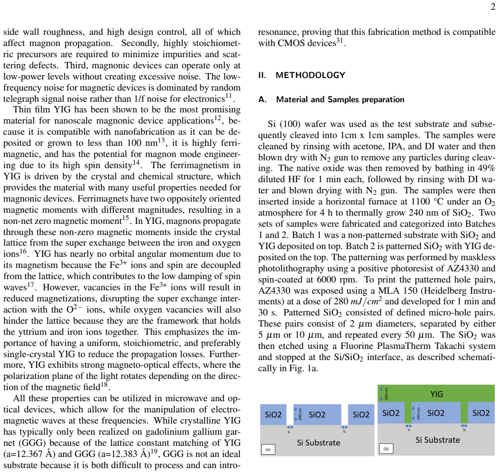
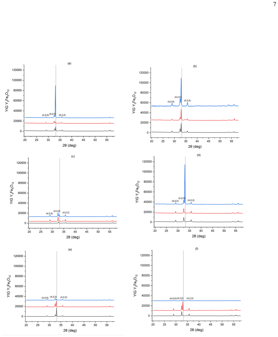
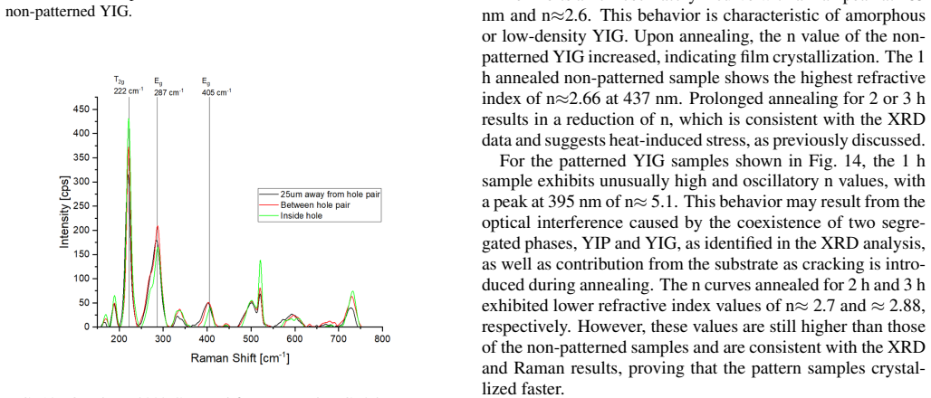
(a) Raman microscope and laser measurement spot inside hole. (b) Between hole pairs. (c) 25µm away from hole pairs. *Note* Contrast and brightness adjusted post imaging. Spectroscopic Ellipsometry (SE) measurements were con- ducted using a J.A Woollam M-2000 to determine both the thickness and optical constants. To characterize thin-film YIG, a modified B...
2000
-
[3]
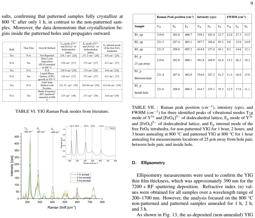
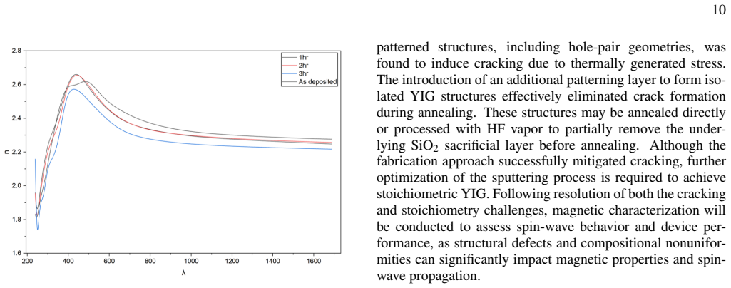
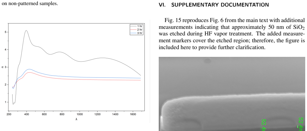
XRD data for hematite with crystal peak (1,0,4) labeled located at 33.23° [36]. TABLE V . XRD 2θposition (°), integrated intensity (cps°), and FWHM (°) data for the YIG (400), (420), Fe 2O3 (104) and YIG (444) for all non-patterned and patterned samples. Table is organized by increasing 2θ. C. Raman Three Raman peaks were identified using fit analysis wit...
2025
-
[4]
Low-field regime of magnon transport in yttrium iron garnet,
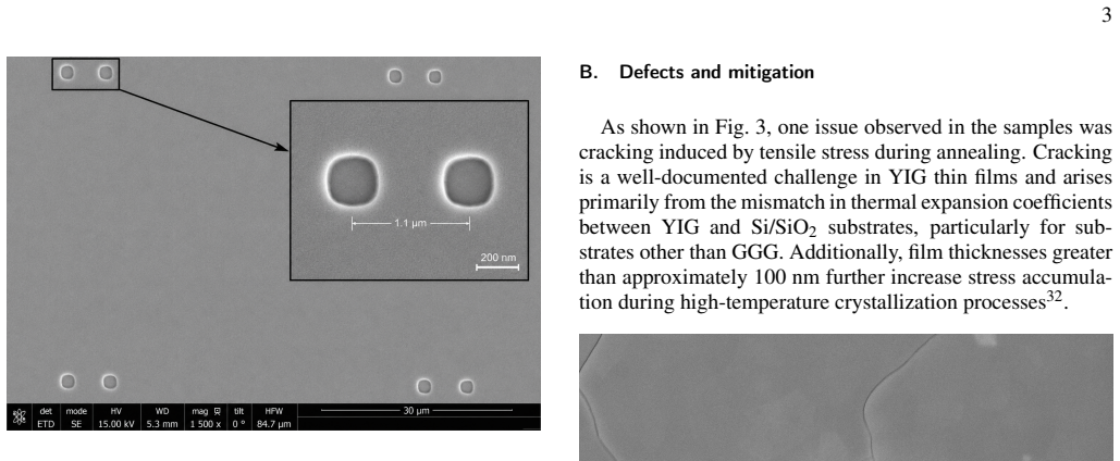
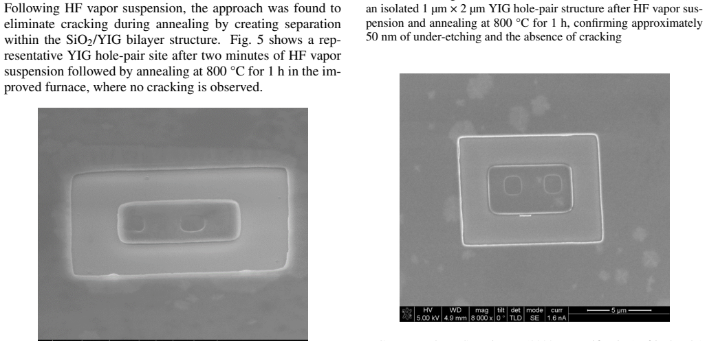
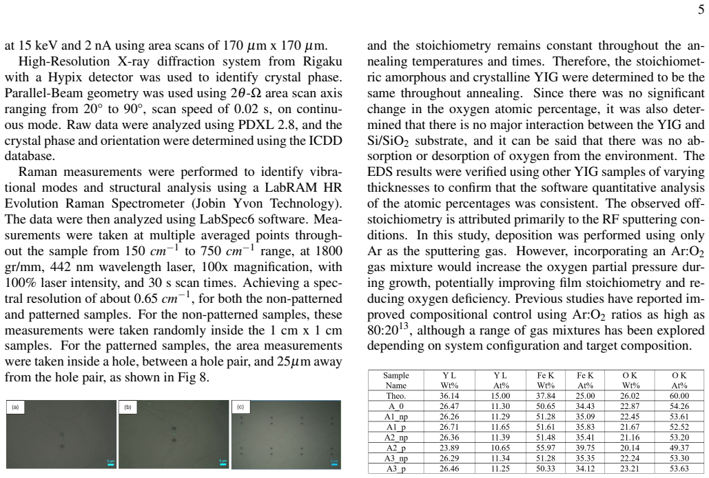
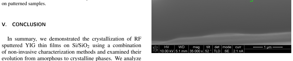
SEM image of Cross-sectional FIB (35000× magnification) of an isolated 1µm × 2µm YIG hole-pair structure after HF vapor suspension and annealing 800 °C for 1 h, confirming approximately 50 nm of under-etching and the absence of cracking with measure- ments. VII. ACKNOWLEDGMENTS This work was performed, in part, at the Center for High Technology Materials ...
-
[5]
2B. Flebuset al., “Recent advances in magnonics,” J. Appl. Phys.133(2023), 10.1063/5.0153424, accessed 21 Jan
-
[6]
Electric field control of chiral magnonic resonators for spin-wave manipulation,
chapter 3 Surface Magnons. 4Y .-Y . Au and K. G. Fripp, “Electric field control of chiral magnonic resonators for spin-wave manipulation,” Phys. Rev. Appl.20(2023), 10.1103/PhysRevApplied.20.034023, accessed 28 Jan
-
[7]
Spin-wave propagation through a magnonic crystal in a thermal gradient,
5T. Langneret al., “Spin-wave propagation through a magnonic crystal in a thermal gradient,” J. Phys. D: Appl. Phys.51, 344002 (2018), accessed 28 Jan
2018
-
[8]
Spin seebeck effect and ballistic transport of quasi- acoustic magnons in room-temperature yttrium iron garnet films,
6T. B. Noacket al., “Spin seebeck effect and ballistic transport of quasi- acoustic magnons in room-temperature yttrium iron garnet films,” J. Phys. D: Appl. Phys.51, 234003 (2018), accessed 28 Jan
2018
-
[9]
Magnon dark modes and gradient memory,
7X. Zhanget al., “Magnon dark modes and gradient memory,” Nat. Com- mun.6(2015), 10.1038/ncomms9914, accessed 24 Oct
-
[10]
Spin-wave propagation in ultra-thin yig based waveg- uides,
8M. Colletet al., “Spin-wave propagation in ultra-thin yig based waveg- uides,” Appl. Phys. Lett.110(2017), 10.1063/1.4976708, accessed 21 Jan
-
[11]
Spin wave modes observation in yig thin films with perpendic- ular magnetic anisotropy,
9Z. Capku, “Spin wave modes observation in yig thin films with perpendic- ular magnetic anisotropy,” J. Magn. Magn. Mater. , 6 (2021). 10T. Matsumoto and T. Homma, “Effect on etch rate and surface roughness of crystal orientation of polycrystalline silicon used for consumable parts of reactive ion etching equipment,” ECS J. Solid State Sci. Technol.11, 08...
2021
-
[12]
The discrete noise of magnons,
11S. Rumyantsevet al., “The discrete noise of magnons,” Appl. Phys. Lett. 114(2019), 10.1063/1.5088651, accessed 28 Jan
-
[13]
Structural and magnetic properties of yig thin films de- posited by pulsed laser deposition and rf magnetron sputtering technique,
12S. Satapathyet al., “Structural and magnetic properties of yig thin films de- posited by pulsed laser deposition and rf magnetron sputtering technique,” Phys. Scr.98, 105508 (2023), accessed 21 Jan
2023
-
[14]
Ultra thin films of yttrium iron garnet with very low damping: A review,
13G. Schmidt, C. Hauser, P. Trempler, M. Paleschke, and E. T. Papaioannou, “Ultra thin films of yttrium iron garnet with very low damping: A review,” Phys. Status Solidi B257, 1900644 (2020). 14M. Settipalliet al., “Investigation of phonon lifetimes and magnon–phonon coupling in yig/ggg hybrid magnonic systems in the diffraction limited regime,” J. Appl. ...
-
[16]
Magnonics: Materials, physics, and devices,
16X. Hanet al., “Magnonics: Materials, physics, and devices,” Appl. Phys. Lett.125(2024), 10.1063/5.0216094, accessed 4 Dec
-
[17]
17W. Nounet al., “Determination of yttrium iron garnet superexchange pa- rameters as a function of oxygen and cation stoichiometry,” Phys. Rev. B 81(2010), 10.1103/physrevb.81.054411, accessed 20 Jan
-
[18]
Integrating magnons for quantum information,
18Z. Jianget al., “Integrating magnons for quantum information,” Appl. Phys. Lett.123(2023), 10.1063/5.0157520, accessed 21 Jan
-
[19]
19M. C. Onbasliet al., “Optical and magneto-optical behavior of cerium yt- trium iron garnet thin films at wavelengths of 200–1770 nm,” Sci. Rep.6 (2016), 10.1038/srep23640, accessed 7 May
-
[20]
Growth of high-quality yttrium iron gar- net thin films on metallic thin layers,
20Y . Sun, Y .-Y . Song, and M. Wu, “Growth of high-quality yttrium iron gar- net thin films on metallic thin layers,” (2011), preprint, Oct
2011
-
[21]
Identification of a new source of magnon relax- ation in interface between epitaxial iron garnet ferrite films and ggg sub- strate,
23A. N. Kuzmichevet al., “Identification of a new source of magnon relax- ation in interface between epitaxial iron garnet ferrite films and ggg sub- strate,” Mater. Res. Bull.149, 111691 (2022), accessed
2022
-
[22]
Monocrystalline freestanding three-dimensional yttrium- iron-garnet magnon nanoresonators,
24F. Heyrothet al., “Monocrystalline freestanding three-dimensional yttrium- iron-garnet magnon nanoresonators,” Phys. Rev. Appl.12, 054031 (2019), accessed
2019
-
[23]
25P. Trempleret al., “Integration and characterization of micron-sized yig structures with very low gilbert damping on arbitrary substrates,” Appl. Phys. Lett.117(2020), 10.1063/5.0026120, accessed 6 Nov
-
[24]
Raman-active phonons in aluminum, gallium, and iron garnets,
26J.-J. Songet al., “Raman-active phonons in aluminum, gallium, and iron garnets,” J. Opt. Soc. Am.63, 1135 (1973), accessed 21 Jan
1973
-
[25]
Pulsed laser deposition grown yttrium-iron-garnet thin films: Effect of composition and iron ion valences on microstructure and magnetic properties,
27L. Jinet al., “Pulsed laser deposition grown yttrium-iron-garnet thin films: Effect of composition and iron ion valences on microstructure and magnetic properties,” Appl. Surf. Sci.483, 947–952 (2019), accessed 21 Jan
2019
-
[26]
Phase transition in y3fe5o12 at high pressures ob- served by raman spectroscopy,
28S. N. Aksenovet al., “Phase transition in y3fe5o12 at high pressures ob- served by raman spectroscopy,” JETP Lett.114, 742–750 (2021), accessed 4 Dec
2021
-
[27]
Crystallization of yttrium-iron garnet (yig) in thin films: Nucleation and growth aspects,
29M. V . Zaezjevet al., “Crystallization of yttrium-iron garnet (yig) in thin films: Nucleation and growth aspects,” MRS Proc.1036(2007), 10.1557/proc-1036-m04-19, accessed 21 Jan
-
[28]
Magneto-optical properties of yttrium iron garnet (yig) thin films elaborated by radio frequency sputtering,
30T. Boudiaret al., “Magneto-optical properties of yttrium iron garnet (yig) thin films elaborated by radio frequency sputtering,” J. Magn. Magn. Mater. 284, 77–85 (2004), accessed 9 Sept
2004
-
[29]
Integration and characterization of micron-sized yig struc- tures with very low gilbert damping on arbitrary substrates,
31P. Trempler, R. Dreyer, P. Geyer, C. Hauser, G. Woltersdorf, and G. Schmidt, “Integration and characterization of micron-sized yig struc- tures with very low gilbert damping on arbitrary substrates,” Appl. Phys. Lett.117, 232401 (2020), accessed
2020
-
[30]
Magneto-optical properties of yttrium iron garnet (yig) thin films elaborated by radio frequency sputtering,
32T. Boudiar, M. Hehn, C. Lacour, M. Klopfer, A. K. Malek, C. Dufour, G. Viau, and F. Montaigne, “Magneto-optical properties of yttrium iron garnet (yig) thin films elaborated by radio frequency sputtering,” Journal of Magnetism and Magnetic Materials284, 77–85 (2004). 33H. Jiang, K. Yoo, J.-L. A. Yeh, Z. Li, and N. C. Tien, “Fabrication of thick silicon ...
2004
-
[31]
Studies on the formation of yttrium iron garnet (yig) through stoichiometry modification prepared by conventional solid-state method,
36W. Zahet al., “Studies on the formation of yttrium iron garnet (yig) through stoichiometry modification prepared by conventional solid-state method,” J. Eur. Ceram. Soc.33, 1317–1324 (2013), accessed 1 May
2013
-
[32]
Effect of post-annealing temperature on the microstructure and magnetic properties of ce:yig thin films deposited on si substrates,
37X. Zhouet al., “Effect of post-annealing temperature on the microstructure and magnetic properties of ce:yig thin films deposited on si substrates,” Appl. Surf. Sci.253, 2108–2112 (2006), accessed 17 May
2006
-
[33]
Data set from: Can laboratory-based xafs compete with xrd and mössbauer spectroscopy by means of quantitative analysis?
38S. Praetzet al., “Data set from: Can laboratory-based xafs compete with xrd and mössbauer spectroscopy by means of quantitative analysis?” (2024), accessed 25 Aug
2024
-
[34]
Raman-active phonons in aluminum, gallium, and iron garnets,
39J.-J. Songet al., “Raman-active phonons in aluminum, gallium, and iron garnets,” J. Opt. Soc. Am.63, 1135 (1973), accessed 21 Jan
1973
-
[35]
Pulsed laser deposition grown yttrium-iron-garnet thin films: Effect of composition and iron ion valences on microstructure and magnetic properties,
40L. Jinet al., “Pulsed laser deposition grown yttrium-iron-garnet thin films: Effect of composition and iron ion valences on microstructure and magnetic properties,” Appl. Surf. Sci.483, 947–952 (2019), accessed 21 Jan
2019
-
[36]
Phase transition in y3fe5o12 at high pressures ob- served by raman spectroscopy,
41S. N. Aksenovet al., “Phase transition in y3fe5o12 at high pressures ob- served by raman spectroscopy,” JETP Lett.114, 742–750 (2021), accessed 4 Dec
2021
-
[37]
Thickness dependence of magnetic properties in submicron yttrium iron garnet films,
42Y . Raoet al., “Thickness dependence of magnetic properties in submicron yttrium iron garnet films,” J. Phys. D: Appl. Phys.51, 435001 (2018), ac- 12 cessed 30 May
2018
-
[38]
Electrical, magnetic, and raman spectroscopic studies on bi-modified yig ceramics,
43T. Susnehaet al., “Electrical, magnetic, and raman spectroscopic studies on bi-modified yig ceramics,” J. Mater. Sci. Mater. Electron.35(2024), 10.1007/s10854-024-12655-9, accessed 30 May
-
[39]
Si raman spectrum,
44RamanLife, “Si raman spectrum,” (2024). 45RamanLife, “Sio2 raman spectrum,” (2024)
2024
discussion (0)
Sign in with ORCID, Apple, or X to comment. Anyone can read and Pith papers without signing in.