Valley Engineering in Bilayer WSe₂ Gate-All-Around Transistors
Pith reviewed 2026-06-27 15:54 UTC · model grok-4.3
The pith
Compressive biaxial strain in bilayer WSe2 raises the on/off current ratio from 69 to 156 while the subthreshold swing stays near 60 mV/dec.
A machine-rendered reading of the paper's core claim, the machinery that carries it, and where it could break.
Core claim
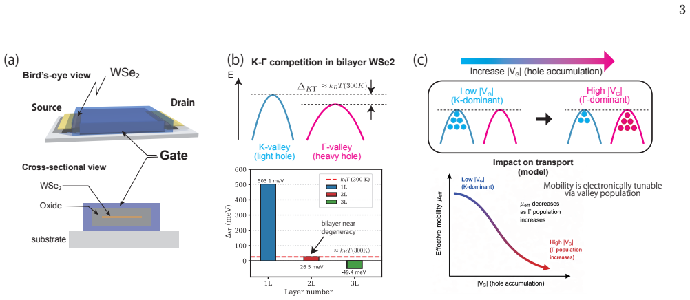
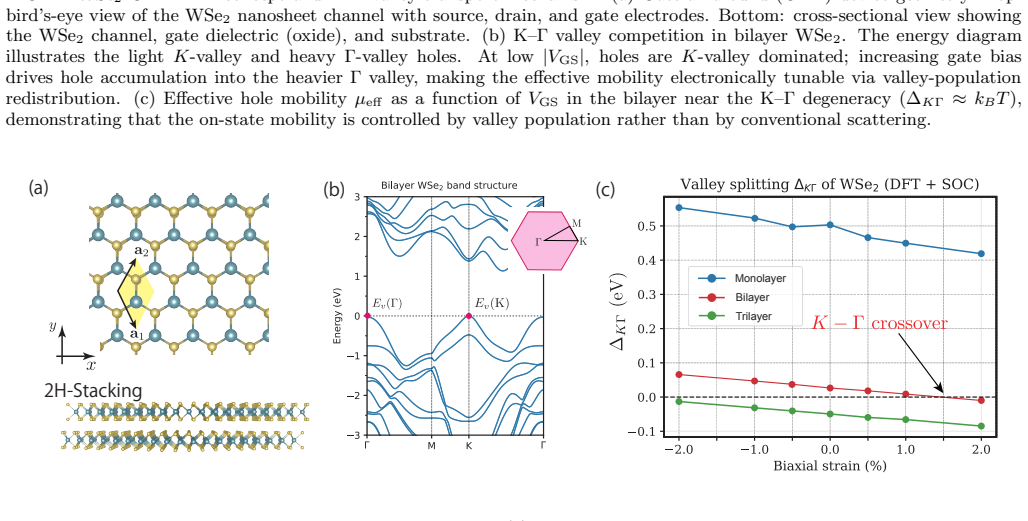
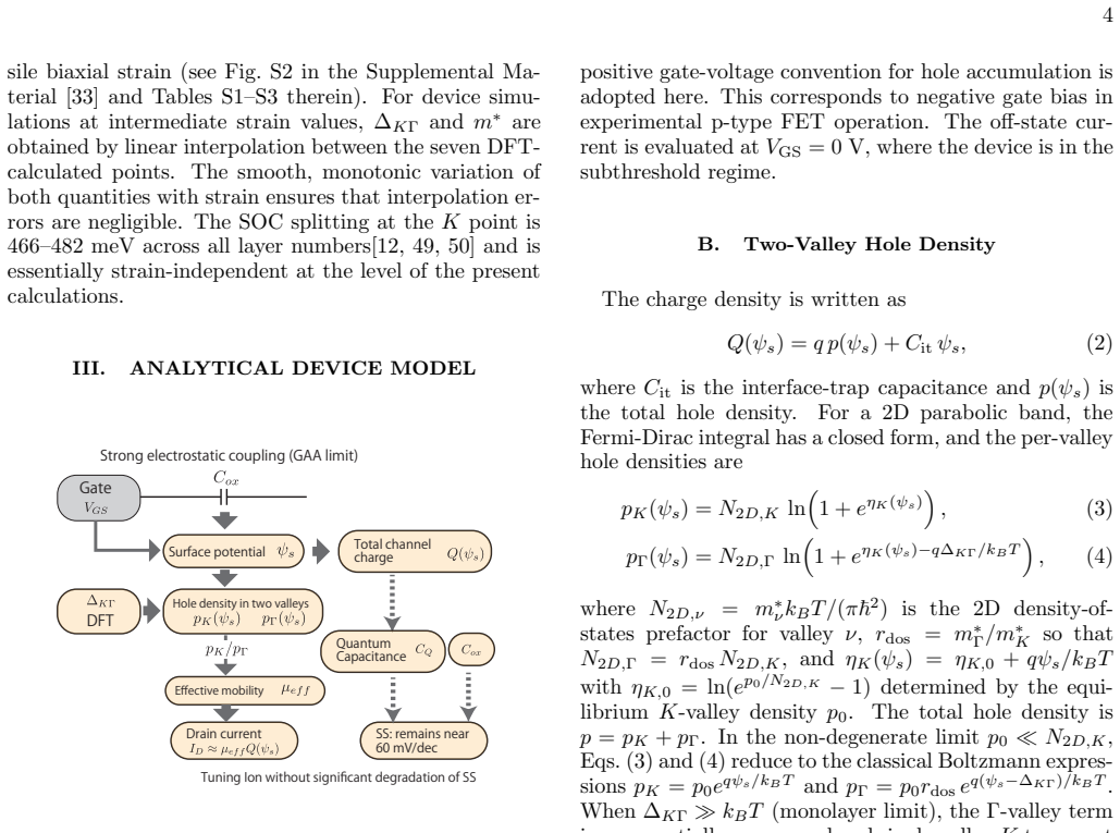
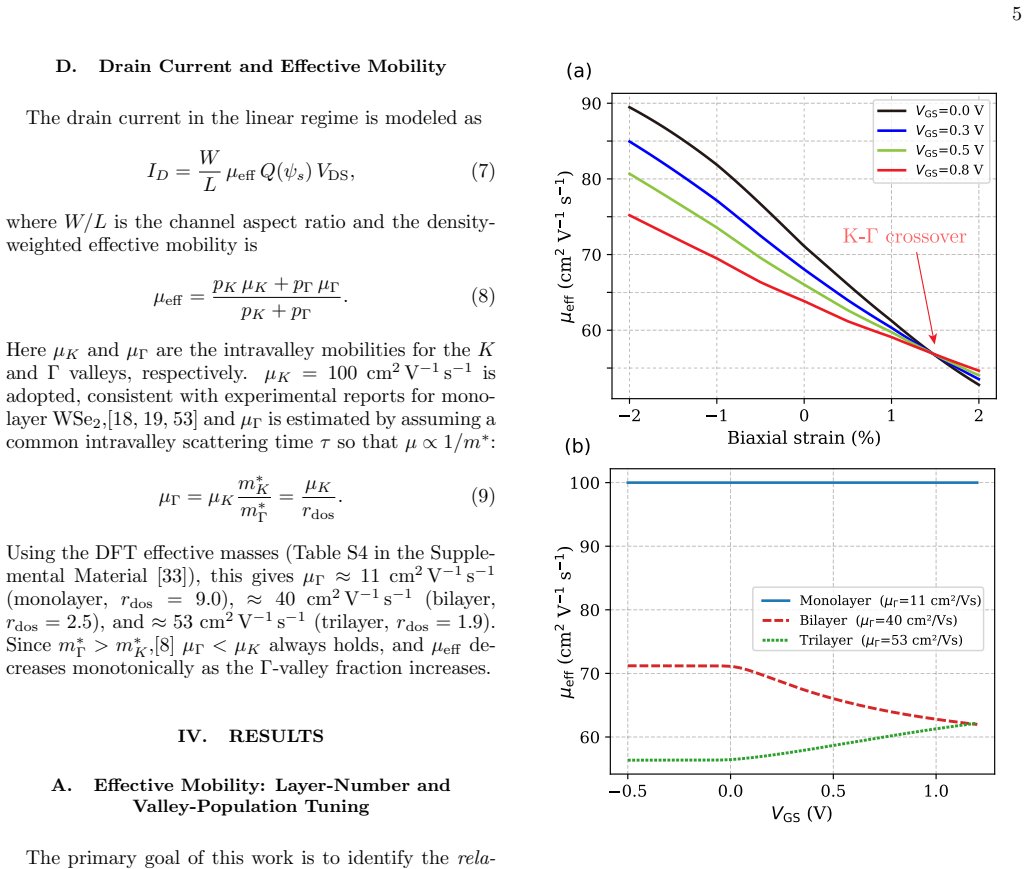
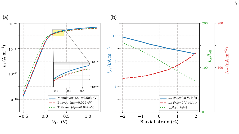
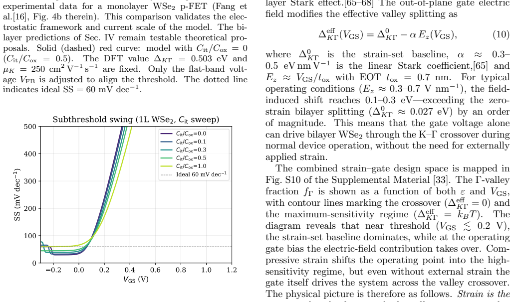
The paper establishes that valley-engineering sensitivity is maximized when the K–Gamma splitting equals kBT, a condition met naturally by bilayer WSe2 at room temperature and zero strain. DFT calculations of valley splitting and effective masses, inserted into an analytical two-valley device model, predict that compressive biaxial strain in the bilayer raises the on-current, lowers the off-current, and improves the on/off ratio from approximately 69 to 156, while the subthreshold swing stays near the thermionic limit. The same model shows that effective mobility falls monotonically with added layers because the valley occupation ratio changes, yet the subthreshold swing itself is independen
What carries the argument
The analytical two-valley device model that treats K and Gamma hole populations as thermally equilibrated channels whose relative occupation is tuned by strain-induced valley splitting.
If this is right
- Subthreshold swing stays near 60 mV/dec independently of layer number because of quantum-capacitance screening.
- Effective mobility is fixed by the K-to-Gamma valley occupation ratio and decreases as layer number increases.
- In the bilayer, compressive strain simultaneously raises on-current and lowers off-current.
- Valley-engineering effects are strongest precisely when the valley splitting is comparable to kBT.
Where Pith is reading between the lines
- The same near-degeneracy condition could be engineered in other few-layer transition-metal dichalcogenides by choosing appropriate thickness or external fields.
- Device models that omit explicit valley splitting may systematically underestimate strain benefits in systems where Delta is near kBT.
- Room-temperature operation of strained bilayer devices would directly test whether the predicted on/off improvement survives scattering mechanisms not captured in the two-valley model.
Load-bearing premise
The analytical two-valley device model, when supplied with DFT-derived valley splittings and masses, quantitatively predicts the strain-induced changes in on- and off-currents for the gate-all-around geometry.
What would settle it
Fabricate a bilayer WSe2 gate-all-around transistor, apply controlled compressive biaxial strain, and measure whether the room-temperature on/off ratio rises from 69 to 156 while the subthreshold swing remains near 60 mV/dec.
Figures
read the original abstract
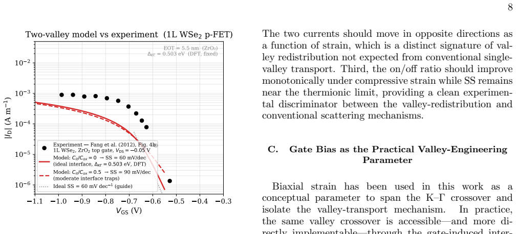
In bilayer WSe$_2$, interlayer coupling reduces the K--$\Gamma$ valley splitting to $\Delta_{K\Gamma} \approx k_BT$ at room temperature, placing two hole-transport channels of markedly different effective mass in near-thermal equilibrium. We combine density functional theory (DFT) with spin--orbit coupling and an analytical two-valley device model to quantify how this near-degeneracy governs hole transport in gate-all-around (GAA) field-effect transistors. Three main results are obtained: (i)~the subthreshold swing is protected near $60$~mV~dec$^{-1}$ by quantum-capacitance screening independently of layer number; (ii)~the effective mobility is set by the K-to-$\Gamma$ valley occupation ratio and decreases monotonically with layer number; and (iii)~in the bilayer, compressive biaxial strain \emph{simultaneously} enhances the on-current, suppresses the off-current, and improves the on/off ratio from ${\approx}69$ to ${\approx}156$, while the subthreshold swing remains near the thermionic limit. This decoupling of on-state performance from switching slope is inaccessible through conventional mobility engineering and establishes a concrete design principle: \emph{valley-engineering sensitivity is maximized when $\Delta_{K\Gamma} \approx k_BT$}, the condition most naturally satisfied by bilayer WSe$_2$ at room temperature and zero strain, making it the optimal channel for valley-engineered GAA transistors.
Editorial analysis
A structured set of objections, weighed in public.
Referee Report
Summary. The manuscript combines DFT calculations (with SOC) and an unspecified analytical two-valley device model to analyze hole transport in bilayer WSe₂ gate-all-around FETs. It reports three results: (i) subthreshold swing remains near 60 mV/dec due to quantum-capacitance screening independent of layer count; (ii) effective mobility is controlled by the K-to-Γ valley occupation ratio and falls with increasing layer number; (iii) compressive biaxial strain in the bilayer simultaneously raises on-current, lowers off-current, and improves the on/off ratio from ≈69 to ≈156 while keeping SS near the thermionic limit. The central design principle is that valley-engineering sensitivity peaks when Δ_{KΓ} ≈ k_B T, a condition naturally met in unstrained bilayer WSe₂.
Significance. If the quantitative predictions of result (iii) can be independently verified, the work would supply a concrete, material-specific route to decouple on-state performance from subthreshold swing in 2D GAA transistors. The identification of bilayer WSe₂ as the layer count that maximizes strain sensitivity at room temperature is a potentially useful design rule, provided the two-valley model is shown to correctly map DFT valley splittings and masses onto GAA electrostatics and currents.
major comments (3)
- [Abstract, results (iii)] Abstract and §3 (results (iii)): the on/off ratio shift from ≈69 to ≈156 under compressive biaxial strain is obtained by feeding DFT-derived Δ_{KΓ} and m* into an analytical two-valley model whose equations, capacitance treatment, and current expressions are never stated. Without these, it is impossible to assess whether the reported numbers follow from the model or are simply re-expressions of the input valley splitting.
- [results (iii)] The two-valley occupation ratio that determines both mobility and the on/off improvement is defined directly from the DFT-computed Δ_{KΓ}. Consequently the strain-induced performance gain reported in result (iii) reduces, by construction, to a restatement of the DFT input rather than an independent prediction of the device model.
- [results (iii)] No validation data, fitting procedure, or comparison against full NEGF or self-consistent Poisson–Schrödinger solutions is provided for the analytical GAA model. Any omitted physics (intervalley scattering, strain dependence of dielectric screening, or short-channel electrostatics beyond the analytical capacitance) would directly change the predicted ratio shift.
minor comments (2)
- The manuscript should include the explicit equations of the two-valley analytical model (current expressions, occupation factors, capacitance model) in a dedicated methods or appendix section.
- Figure captions and text should clarify whether the quoted on/off values are obtained at fixed gate overdrive or at fixed off-current, and at what drain bias.
Simulated Author's Rebuttal
We thank the referee for the careful reading and constructive comments on our manuscript. We address each major comment below and indicate the revisions that will be incorporated.
read point-by-point responses
-
Referee: [Abstract, results (iii)] Abstract and §3 (results (iii)): the on/off ratio shift from ≈69 to ≈156 under compressive biaxial strain is obtained by feeding DFT-derived Δ_{KΓ} and m* into an analytical two-valley model whose equations, capacitance treatment, and current expressions are never stated. Without these, it is impossible to assess whether the reported numbers follow from the model or are simply re-expressions of the input valley splitting.
Authors: We agree that the equations of the analytical two-valley model were not presented explicitly. In the revised manuscript we will add a dedicated subsection (or supplementary note) that states the full set of model equations, including the expressions for valley occupation, quantum capacitance in the GAA geometry, and the resulting current. This will allow direct verification that the reported on/off ratios are obtained from the model rather than being direct restatements of the DFT inputs. revision: yes
-
Referee: [results (iii)] The two-valley occupation ratio that determines both mobility and the on/off improvement is defined directly from the DFT-computed Δ_{KΓ}. Consequently the strain-induced performance gain reported in result (iii) reduces, by construction, to a restatement of the DFT input rather than an independent prediction of the device model.
Authors: While Δ_{KΓ} is taken from DFT, the device model independently maps this splitting onto electrostatics and transport. The occupation ratio enters the GAA capacitance and current expressions together with the distinct effective masses of the two valleys; the strain-induced change in on- and off-currents therefore emerges from the solution of the model equations rather than from the DFT value alone. We will clarify this distinction in the revised text. revision: no
-
Referee: [results (iii)] No validation data, fitting procedure, or comparison against full NEGF or self-consistent Poisson–Schrödinger solutions is provided for the analytical GAA model. Any omitted physics (intervalley scattering, strain dependence of dielectric screening, or short-channel electrostatics beyond the analytical capacitance) would directly change the predicted ratio shift.
Authors: We acknowledge that the analytical model has not been benchmarked against NEGF or self-consistent simulations. In the revision we will add an explicit discussion of the model’s assumptions and the possible quantitative impact of omitted effects such as intervalley scattering. The model is intended to isolate the valley-engineering mechanism; the reported numbers should be understood as indicative of the design principle rather than precise device predictions. revision: partial
Circularity Check
No circularity; derivation uses external DFT inputs in independent analytical model
full rationale
The paper computes valley splitting ΔKΓ and effective masses via DFT (external first-principles calculation), then inserts those values into a separate analytical two-valley device model to obtain on/off currents and ratios under strain. No equation in the abstract or described results equates a model output directly to an input by algebraic identity or by renaming a fitted parameter as a prediction. No self-citations appear in the load-bearing steps, and the central claim (iii) is a forward calculation from the combined inputs rather than a self-definition or tautology. This is the normal, non-circular workflow of parameter extraction followed by device modeling.
Axiom & Free-Parameter Ledger
free parameters (2)
- K-to-Γ valley occupation ratio
- compressive biaxial strain value
axioms (2)
- domain assumption The analytical two-valley device model accurately maps valley occupation to on- and off-currents in the GAA geometry
- domain assumption Quantum-capacitance screening protects subthreshold swing near 60 mV/dec independently of layer number
Forward citations
Cited by 1 Pith paper
-
Electrical Spectroscopy of Intervalley Relaxation in WSe$_2$ Transistors
Transconductance in multilayer WSe2 FETs acts as an electrical spectrometer for intervalley relaxation time τ_iv via predicted Lorentzian frequency response, two-stage transients, and sweep-rate hysteresis with layer-...
Reference graph
Works this paper leans on
-
[1]
Xiao, G.-B
D. Xiao, G.-B. Liu, W. Feng, X. Xu, and W. Yao, Cou- pled spin and valley physics in monolayers of MoS 2 and other group-VI dichalcogenides, Phys. Rev. Lett.108, 196802 (2012)
2012
-
[2]
Manzeli, D
S. Manzeli, D. Ovchinnikov, D. Pasquier, O. V. Yazyev, and A. Kis, 2D transition metal dichalcogenides, Nat. Rev. Mater.2, 17033 (2017)
2017
-
[3]
K. S. Novoselov, A. Mishchenko, A. Carvalho, and A. H. Castro Neto, 2D materials and van der Waals het- erostructures, Science353, aac9439 (2016)
2016
-
[4]
A. K. Geim and I. V. Grigorieva, Van der Waals het- erostructures, Nature499, 419 (2013)
2013
-
[5]
S. Lai, Z. Zhang, N. Wang, A. Rasmita, Y. Deng, Z. Liu, and W.-B. Gao, Dual-gate all-electrical valleytronic tran- sistors, Nano Lett.23, 192 (2023)
2023
-
[6]
W. Zhao, Z. Ghorannevis, L. Chu, M. Toh, C. Kloc, P.- H. Tan, and G. Eda, Evolution of electronic structure in atomically thin sheets of WS 2 and WSe2, ACS Nano7, 791 (2013)
2013
-
[7]
Zhang, T.-R
Y. Zhang, T.-R. Chang, B. Zhou, Y.-T. Cui, H. Yan, Z. Liu, F. Schmitt, J. Lee, R. Moore, Y. Chen, H. Lin, H.-T. Jeng, S.-K. Mo, Z. Hussain, A. Bansil, and Z.-X. Shen, Direct observation of the transition from indirect to direct bandgap in atomically thin epitaxial MoSe 2, Nat. Nanotechnol.9, 111 (2014)
2014
-
[8]
Wickramaratne, F
D. Wickramaratne, F. Zahid, and R. K. Lake, Elec- tronic and thermoelectric properties of few-layer transi- tion metal dichalcogenides, J. Chem. Phys.140, 124710 (2014)
2014
-
[9]
P.-C. Yeh, W. Jin, N. Zaki, D. Zhang, J. T. Liou, J. T. Sadowski, A. Al-Mahboob, J. I. Dadap, I. P. Herman, P. Sutter, and J. Osgood, R. M., Layer-dependent elec- tronic structure of an atomically heavy two-dimensional dichalcogenide, Phys. Rev. B91, 041407 (2015)
2015
-
[10]
Korm´ anyos, G
A. Korm´ anyos, G. Burkard, M. Gmitra, J. Fabian, V. Z´ olyomi, N. D. Drummond, and V. Fal’ko, k·p the- ory for two-dimensional transition metal dichalcogenide semiconductors, 2D Mater.2, 022001 (2015)
2015
-
[11]
Ridolfi, D
E. Ridolfi, D. Le, T. S. Rahman, E. R. Mucciolo, and C. H. Lewenkopf, A tight-binding model for MoS2 mono- layers, J. Phys.: Condens. Matter27, 365501 (2015)
2015
-
[12]
Z. Y. Zhu, Y. C. Cheng, and U. Schwingenschl¨ ogl, Gi- ant spin-orbit-induced spin splitting in two-dimensional transition-metal dichalcogenide semiconductors, Phys. Rev. B84, 153402 (2011)
2011
-
[13]
H. C. P. Movva, T. Lovorn, B. Fallahazad, S. Laren- tis, K. Kim, T. Taniguchi, K. Watanabe, S. K. Baner- jee, A. H. MacDonald, and E. Tutuc, Tunable Γ–Kval- ley populations in hole-doped trilayer WSe 2, Phys. Rev. Lett.120, 107703 (2018)
2018
-
[14]
Z. Jin, X. Li, J. T. Mullen, and K. W. Kim, Intrin- sic transport properties of electrons and holes in mono- layer transition metal dichalcogenides, Phys. Rev. B90, 045422 (2014)
2014
-
[15]
X. Xu, W. Yao, D. Xiao, and T. F. Heinz, Spin and pseudospins in layered transition metal dichalcogenides, Nat. Phys.10, 343 (2014)
2014
-
[16]
H. Fang, S. Chuang, T. C. Chang, K. Takei, T. Taka- hashi, and A. Javey, High-performance single layered WSe2 p-FETs with chemically doped contacts, Nano Lett.12, 3788 (2012)
2012
-
[17]
W. Liu, J. Kang, D. Sarkar, Y. Khatami, D. Jena, and K. Banerjee, Role of metal contacts in designing high- performance monolayer n-type WSe 2 field effect transis- tors, Nano Lett.13, 1983 (2013)
1983
-
[18]
Allain and A
A. Allain and A. Kis, Electron and hole mobilities in single-layer WSe2, ACS Nano8, 7180 (2014)
2014
-
[19]
N. R. Pradhan, D. Rhodes, S. Memaran, J. M. Poumirol, D. Smirnov, S. Talapatra, S. Feng, N. Perea-Lopez, A. L. Elias, M. Terrones, P. M. Ajayan, and L. Balicas, Hall and field-effect mobilities in few layered p-WSe 2 field- effect transistors, Sci. Rep.5, 8979 (2015)
2015
-
[20]
N. H. Patoary, J. Xie, G. Zhou, F. Al Mamun, M. Sayyad, S. Tongay, and I. Sanchez Esqueda, Improvements in 2D p-type WSe2 transistors towards ultimate CMOS scaling, Sci. Rep.13, 3304 (2023)
2023
-
[21]
Chiu, W.-C
K.-H. Chiu, W.-C. Wu, H.-Y. Huang, J.-H. Chih, Y.-C. Chang, S.-T. Wang, H.-Y. Chen, C.-Y. Lin, D.-H. Lien, C. Hu, and C.-H. Chien, Homo-channel WSe 2 n/pFETs with high performance and on/off ratio using tunable doping, inSymp. VLSI Technology and Circuits(2025)
2025
-
[22]
Ghosh, M
S. Ghosh, M. U. K. Sadaf, A. R. Graves, Y. Zheng, A. Pannone, S. Ray, C. Y. Cheng, J. Guevara, J. M. Redwing, and S. Das, High-performance p-type bilayer WSe2 field effect transistors by nitric oxide doping, Nat. Commun.16, 5649 (2025)
2025
-
[23]
Loubet, T
N. Loubet, T. Hook, P. Montanini, C.-W. Yeung, S. Kanakasabapathy, M. Guillorn, T. Yamashita, J. Zhang, X. Miao, J. Wang, A. Young, R. Chao, M. Kang, Z. Liu, S. Fan, B. Hamieh, S. Sieg, Y. Mignot, W. Xu, S.-C. Seo, J. Yoo, S. Mochizuki, M. Sankarapan- dian, O. Kwon, A. Carr, A. Greene, Y. Park, J. Frougier, R. Galatage, R. Bao, J. Shearer, R. Conti, H. So...
2017
-
[24]
A. M. Ionescu and H. Riel, Tunnel field-effect transistors as energy-efficient electronic switches, Nature479, 329 (2011)
2011
-
[25]
Mukesh and J
S. Mukesh and J. Zhang, A review of the gate-all-around nanosheet FET process opportunities, Electronics11, 3589 (2022)
2022
-
[26]
S. B. Desai, S. R. Madhvapathy, A. B. Sachid, J. P. Lli- nas, Q. Wang, G. H. Ahn, G. Pitner, M. J. Kim, J. Bokor, C. Hu, H.-S. P. Wong, and A. Javey, MoS 2 transistors with 1-nanometer gate lengths, Science354, 99 (2016)
2016
-
[27]
S. Das, A. Sebastian, E. Pop, C. J. McClellan, A. D. Franklin, T. Grasser, T. Knobloch, Y. Illarionov, A. V. Penumatcha, J. Appenzeller, Z. Chen, W. Zhu, I. Assel- berghs, L.-J. Li, U. E. Avci, N. Bhat, T. D. Anthopoulos, and R. Singh, Transistors based on two-dimensional ma- terials for future integrated circuits, Nat. Electron.4, 786 (2021)
2021
-
[28]
Fiori, F
G. Fiori, F. Bonaccorso, G. Iannaccone, T. Pala- cios, D. Neumaier, A. Seabaugh, S. K. Banerjee, and L. Colombo, Electronics based on two-dimensional ma- 11 terials, Nat. Nanotechnol.9, 768 (2014)
2014
-
[29]
Zheng, W
F. Zheng, W. Meng, and L.-J. Li, Continue the scaling of electronic devices with transition metal dichalcogenide semiconductors, Nano Lett.25, 3683 (2025)
2025
-
[30]
Chen, M.-Y
J. Chen, M.-Y. Sun, Z.-H. Wang, Z. Zhang, K. Zhang, S. Wang, Y. Zhang, X. Wu, T.-L. Ren, H. Liu, and L. Han, Performance limits and advancements in sin- gle 2D transition metal dichalcogenide transistor, Nano- Micro Lett.16, 264 (2024)
2024
-
[31]
M¨ uller, T
J. M¨ uller, T. S. B¨ oscke, U. Schr¨ oder, S. Mueller, D. Br¨ auhaus, U. B¨ ottger, L. Frey, and T. Mikolajick, Ferroelectricity in simple binary ZrO 2 and HfO 2, Nano Lett.12, 4318 (2012)
2012
-
[32]
Lin, B.-C
C.-Y. Lin, B.-C. Chen, Y.-C. Liu, S.-F. Kuo, H.-C. Tsai, Y.-M. Chang, C.-Y. Kuo, C.-F. Chang, J.-H. Chen, Y.- H. Chu, M. Yamamoto, C.-H. Shen, Y.-L. Chueh, P.-W. Chiu, Y.-C. Chen, J.-C. Yang, and Y.-F. Lin, Integra- tion of freestanding hafnium zirconium oxide membranes into two-dimensional transistors as a high-κferroelectric dielectric, Nat. Electron.8,...
2025
-
[33]
See Supplemental Material at [URL will be in- serted by publisher] for DFT computational details, band structures, effective-mass tables, Γ-valley fraction, subthreshold-swing analysis,I D–VGS characteristics un- der strain and interface traps, saturation model, short- channel effects, and gate-field Stark analysis
-
[34]
K. He, C. Poole, K. F. Mak, and J. Shan, Experimental demonstration of continuous electronic structure tuning via strain in atomically thin MoS 2, Nano Lett.13, 2931 (2013)
2013
-
[35]
H. J. Conley, B. Wang, J. I. Ziegler, R. F. Haglund, Jr., S. T. Pantelides, and K. I. Bolotin, Bandgap engineering of strained monolayer and bilayer MoS 2, Nano Lett.13, 3626 (2013)
2013
-
[36]
Johari and V
P. Johari and V. B. Shenoy, Tuning the electronic prop- erties of semiconducting transition metal dichalcogenides by applying mechanical strains, ACS Nano6, 5449 (2012)
2012
-
[37]
Scalise, M
E. Scalise, M. Houssa, G. Pourtois, V. Afanas’ev, and A. Stesmans, Strain-induced semiconductor to metal transition in the two-dimensional honeycomb structure of MoS2, Nano Res.5, 43 (2012)
2012
-
[38]
Kumar, L
A. Kumar, L. Xu, A. Pal, K. Agashiwala, K. Parto, W. Cao, and K. Banerjee, Strain engineering in 2D FETs: Physics, status, and prospects, J. Appl. Phys. 136, 090901 (2024)
2024
-
[39]
Michail, J
A. Michail, J. A. Yang, K. Filintoglou, N. Balakeras, C. A. Nattoo, C. S. Bailey, A. Daus, J. Parthenios, E. Pop, and K. Papagelis, Biaxial strain transfer in mono- layer MoS2 and WSe 2 transistor structures, ACS Appl. Mater. Interfaces16, 49602 (2024)
2024
-
[40]
G. H. Ahn, M. Amani, H. Rasool, D.-H. Lien, J. P. Ma- standrea, J. W. Ager, M. Dubey, D. C. Chrzan, A. M. Minor, and A. Javey, Strain-engineered growth of two- dimensional materials, Nat. Commun.8, 608 (2017)
2017
-
[41]
Carrascoso, H
F. Carrascoso, H. Li, R. Frisenda, and A. Castellanos- Gomez, Strain engineering in single-, bi- and tri-layer MoS2, MoSe 2, WS 2 and WSe 2, Nano Res.14, 1698 (2021)
2021
-
[42]
Jaikissoon, C ¸
M. Jaikissoon, C ¸ . K¨ oro˘ glu, J. A. Yang, K. M. Neilson, K. C. Saraswat, and E. Pop, CMOS-compatible strain en- gineering for monolayer semiconductor transistors, Nat. Electron.7, 885 (2024)
2024
-
[43]
Kresse and J
G. Kresse and J. Furthm¨ uller, Efficient iterative schemes forAb Initiototal-energy calculations using a plane-wave basis set, Phys. Rev. B54, 11169 (1996)
1996
-
[44]
Kresse and J
G. Kresse and J. Furthm¨ uller, Efficiency ofAb Initiototal energy calculations for metals and semiconductors using a plane-wave basis set, Comput. Mater. Sci.6, 15 (1996)
1996
-
[45]
J. P. Perdew, K. Burke, and M. Ernzerhof, Generalized gradient approximation made simple, Phys. Rev. Lett. 77, 3865 (1996)
1996
-
[46]
Grimme, J
S. Grimme, J. Antony, S. Ehrlich, and H. Krieg, A con- sistent and accurateAb Initioparametrization of density functional dispersion correction (DFT-D) for the 94 ele- ments H–Pu, J. Chem. Phys.132, 154104 (2010)
2010
-
[47]
Komsa and A
H.-P. Komsa and A. V. Krasheninnikov, Effects of con- finement and environment on the electronic structure and exciton binding energy of MoS2 from first principles, Phys. Rev. B86, 241201 (2012)
2012
-
[48]
D. Muoi, N. N. Hieu, H. T. T. Phung, H. V. Phuc, B. Amin, B. D. Hoi, N. V. Hieu, L. C. Nhan, C. V. Nguyen, and P. T. T. Le, Electronic properties of WS 2 and WSe 2 monolayers with biaxial strain: A first- principles study, Chem. Phys.519, 69 (2019)
2019
-
[49]
J. M. Riley, F. Mazzola, M. Dendzik, M. Michiardi, T. Takayama, L. Bawden, C. Granerød, M. Leandersson, T. Balasubramanian, M. Hoesch, T. K. Kim, H. Tak- agi, W. Meevasana, P. Hofmann, M. S. Bahramy, J. W. Wells, and P. D. C. King, Direct observation of spin- polarized bulk bands in an inversion-symmetric semicon- ductor, Nat. Phys.10, 835 (2014)
2014
-
[50]
D. Le, A. Barinov, E. Preciado, M. Isarraraz, I. Tanabe, T. Komesu, C. Troha, L. Bartels, T. S. Rahman, and P. A. Dowben, Spin–orbit coupling in the band struc- ture of monolayer WSe 2, J. Phys.: Condens. Matter27, 182201 (2015)
2015
-
[51]
Luryi, Quantum capacitance devices, Appl
S. Luryi, Quantum capacitance devices, Appl. Phys. Lett. 52, 501 (1988)
1988
-
[52]
R. K. A. Bennett and E. Pop, How do quantum effects in- fluence the capacitance and carrier density of monolayer MoS2 transistors?, Nano Lett.23, 1666 (2023)
2023
-
[53]
V.-A. Ha, S. Tiwari, and F. Giustino, Ultrahigh hole mobility in monolayer WSe 2 enabled by spin–orbit sup- pression of intervalley scattering, Nano Lett.25, 14304 (2025)
2025
-
[54]
S. B. Desai, G. Seol, J. S. Kang, H. Fang, C. Battaglia, R. Kapadia, J. W. Ager, J. Guo, and A. Javey, Strain- induced indirect to direct bandgap transition in multi- layer WSe2, Nano Lett.14, 4592 (2014)
2014
-
[55]
C. S. Boland, Y. Sun, and D. G. Papageorgiou, Bandgap engineering of 2D materials toward high-performing straintronics, Nano Lett.24, 12722 (2024)
2024
-
[56]
X. Yang, S. Fang, Y. Li, Z. Yang, Q. Li, M. Wang, and J. Lu, Ab-initio quantum transport simulation of sub-1 nm gate length monolayer and bilayer WSe 2 tran- sistors: Implications for ultra-scaled CMOS technology, ACS Appl. Nano Mater.8, 3460 (2025)
2025
-
[57]
Chuang, X
H.-J. Chuang, X. Tan, N. J. Ghimire, M. M. Perera, B. Chamlagain, M. M.-C. Cheng, J. Yan, D. Mandrus, D. Tom´ anek, and Z. Zhou, High mobility WSe2 p- and n-type field-effect transistors contacted by highly doped graphene for low-resistance contacts, Nano Lett.14, 3594 (2014)
2014
-
[58]
Tosun, S
M. Tosun, S. Chuang, H. Fang, A. B. Sachid, M. Hettick, Y. Lin, Y. Zeng, and A. Javey, High-gain inverters based on WSe 2 complementary field-effect transistors, ACS 12 Nano8, 4948 (2014)
2014
-
[59]
F. Ali, H. Choi, N. Ali, Y. Hassan, T. D. Ngo, F. Ahmed, W. K. Park, Z. Sun, and W. J. Yoo, Achieving near-ideal subthreshold swing in p-type WSe 2 field-effect transis- tors, Adv. Electron. Mater.10, 2400071 (2024)
2024
-
[60]
Lee, Y.-C
T.-E. Lee, Y.-C. Su, B.-J. Lin, Y.-X. Chen, W.-S. Yun, P.-H. Ho, J.-F. Wang, S.-K. Su, C.-F. Hsu, P.-S. Mao, Y.-C. Chang, C.-H. Chien, B.-H. Liu, C.-Y. Su, C.-C. Kei, H. Wang, H.-S. P. Wong, T. Y. Lee, W.-H. Chang, C.-C. Cheng, and I. P. Radu, Nearly ideal subthreshold swing in monolayer MoS2 top-gate nfets with scaled EOT of 1 nm, Tech. Dig. Int. Electro...
2022
-
[61]
Y. Y. Illarionov, T. Knobloch, M. Jech, M. Lanza, D. Akinwande, M. I. Vexler, T. Mueller, M. C. Lemme, G. Fiori, F. Schwierz, and T. Grasser, Insulators for 2D nanoelectronics: The gap to bridge, Nat. Commun.11, 3385 (2020)
2020
-
[62]
Huang, Y
X. Huang, Y. Yao, S. Peng, D. Zhang, J. Shi, and Z. Jin, Effects of charge trapping at the MoS2–SiO2 interface on the stability of subthreshold swing of MoS 2 field effect transistors, Materials13, 2896 (2020)
2020
-
[63]
Ghatak, S
S. Ghatak, S. Mukherjee, M. Jain, D. D. Sarma, and A. Ghosh, Microscopic origin of low frequency noise in MoS 2 field-effect transistors, APL Mater.2, 092515 (2014)
2014
-
[64]
Liang, L
B. Liang, L. Liu, J. Tang, J. Chen, Y. Shi, and S. Li, Enhancement of carrier mobility in semiconductor nanos- tructures by carrier distribution engineering, Chin. Phys. Lett.40, 058503 (2023)
2023
-
[65]
Ramasubramaniam, D
A. Ramasubramaniam, D. Naveh, and E. Towe, Tunable band gaps in bilayer transition-metal dichalcogenides, Phys. Rev. B84, 205325 (2011)
2011
-
[66]
C. Gong, H. Zhang, W. Wang, L. Colombo, R. M. Wal- lace, and K. Cho, Band alignment of two-dimensional transition metal dichalcogenides: Application in tunnel field effect transistors, Appl. Phys. Lett.103, 053513 (2013)
2013
-
[67]
Zhang, J
Z. Zhang, J. Li, G. Yang, and G. Ouyang, Interface engi- neering of band evolution and transport properties of bi- layer WSe2 under different electric fields, J. Phys. Chem. C123, 19812 (2019)
2019
-
[68]
L. Wei, Q. Li, M. U. Rehman, Y. He, D. An, S. Li, K. Watanabe, T. Taniguchi, M. Claassen, K. S. Novoselov, D. M. Kennes, A. Rubio, D. A. Rhodes, L. Xian, G. Yu, and L. Wang, Valley charge-transfer in- sulator in twisted double bilayer WSe 2, Nat. Commun. 16, 1185 (2025)
2025
-
[69]
Fivaz and E
R. Fivaz and E. Mooser, Mobility of charge carriers in semiconducting layer structures, Phys. Rev.163, 743 (1967)
1967
-
[70]
J. R. Schaibley, H. Yu, G. Clark, P. Rivera, J. S. Ross, K. L. Seyler, W. Yao, and X. Xu, Valleytronics in 2D materials, Nat. Rev. Mater.1, 16055 (2016)
2016
-
[71]
Allain, J
A. Allain, J. Kang, K. Banerjee, and A. Kis, Electrical contacts to two-dimensional semiconductors, Nat. Mater. 14, 1195 (2015)
2015
-
[72]
Das, H.-Y
S. Das, H.-Y. Chen, A. V. Penumatcha, and J. Ap- penzeller, High performance multilayer MoS 2 transistors with scandium contacts, Nano Lett.13, 100 (2013)
2013
discussion (0)
Sign in with ORCID, Apple, or X to comment. Anyone can read and Pith papers without signing in.