The origin and promise of transition metal dichalcogenide hosted single photon emitters for quantum technologies
Pith reviewed 2026-05-10 06:32 UTC · model grok-4.3
The pith
Critical review of disputed atomic origins for single photon emitters in TMDCs clarifies their source and needed improvements for quantum use.
A machine-rendered reading of the paper's core claim, the machinery that carries it, and where it could break.
Core claim
The atomistic origin of single photon emitters in TMDCs is highly debated with contradicting proposals; a critical review of these proposals, trend analysis of figures of merit, and a proposed characterization methodology can elucidate their origin and streamline reporting for quantum technology adoption.
What carries the argument
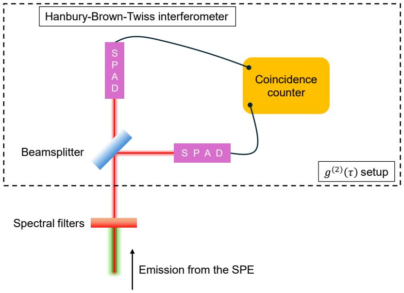
Critical synthesis of atomistic proposals for the origin of single photon emission in TMDC monolayers, supported by statistical trend analysis of device performance metrics and a recommended characterization protocol.
Load-bearing premise
The published experimental data on TMDC-hosted single photon emitters is complete, consistent, and free of significant reporting biases, allowing a reliable critical synthesis.
What would settle it
A large-scale controlled experiment that systematically varies atomic defects in multiple TMDC materials and finds emission statistics that match none of the reviewed origin proposals, or a meta-analysis of additional papers that shows no reproducible performance trends across studies.
Figures


read the original abstract
Single photon emitters (SPEs) are integral parts of several quantum technology implementations. Over the past decade or so, monolayers of transition metal dichalcogenides (TMDCs) have emerged as one of the promising candidates for SPE platforms with attractive characteristics. To move ahead, it is necessary to understand the atomistic origin of SPEs in TMDCs - a topic which is highly debated with contradicting proposals. In this paper, we critically review these existing proposals to elucidate their origin. Further, we perform a critical trend analysis for different figures of merit of TMDC-based SPEs, and propose a characterization methodology to streamline the reporting process. Finally, we review several quantum technology implementations where solid state SPEs are being used, and identify the advancements required in TMDC-based SPEs for their successful adoption in these technologies.
Editorial analysis
A structured set of objections, weighed in public.
Referee Report
Summary. The manuscript is a critical review of the highly debated atomistic origins of single-photon emitters (SPEs) hosted in transition metal dichalcogenide (TMDC) monolayers. It synthesizes conflicting proposals from the literature, performs a trend analysis of key figures of merit (e.g., brightness, purity, and stability), proposes a standardized characterization methodology to improve reporting consistency, and reviews quantum technology applications while identifying performance gaps for TMDC SPE adoption.
Significance. If the literature synthesis is robust, the work could help consolidate fragmented understanding of SPE origins in TMDCs and provide practical guidance for experimental standardization, which is a noted weakness in the field. The proposed characterization protocol directly addresses reproducibility issues, and the mapping to quantum technology requirements (e.g., for communication or sensing) offers a useful roadmap. These elements have the potential to streamline future research and accelerate technology transfer, provided the trend analysis accounts for experimental variability.
major comments (2)
- [Trend analysis section] Trend analysis section: The paper performs a critical trend analysis of figures of merit but does not describe explicit controls, normalization procedures, or exclusion criteria for confounding variables such as differing excitation wavelengths, substrate interactions, sample quality metrics, or inconsistent defect identification techniques across the compiled experimental reports. Without these, observed trends risk reflecting methodological heterogeneity rather than intrinsic atomistic physics, directly undermining the central claim that the review elucidates SPE origins.
- [Review of origin proposals] Review of origin proposals: While the manuscript critically reviews contradicting proposals for the atomistic origin of TMDC SPEs, it lacks a systematic comparison (e.g., a summary table or weighted evidence assessment) that maps specific experimental observables (such as temperature dependence, magnetic field response, or defect spectroscopy) to each proposed model. This omission makes it difficult to evaluate the relative strength of evidence and weakens the elucidation of origins.
minor comments (3)
- [Abstract] Abstract: The phrase 'over the past decade or so' is vague; specifying the exact literature search period, database used, or approximate number of papers reviewed would improve transparency and context for the synthesis.
- [Characterization methodology proposal] Characterization methodology proposal: The proposed protocol would be more actionable if presented as a concise checklist or flowchart rather than descriptive text, and if it included references to standard measurement techniques or example datasets.
- [Quantum technology implementations section] Quantum technology implementations section: Some cited performance targets for applications (e.g., indistinguishability thresholds) could be cross-referenced to specific TMDC FoM trends to make the 'advancements required' discussion more quantitative.
Simulated Author's Rebuttal
We thank the referee for their constructive and detailed comments, which identify opportunities to strengthen the methodological transparency of our trend analysis and the systematic presentation of evidence in our review of origin proposals. We address each major comment below and will incorporate the suggested improvements in the revised manuscript.
read point-by-point responses
-
Referee: [Trend analysis section] Trend analysis section: The paper performs a critical trend analysis of figures of merit but does not describe explicit controls, normalization procedures, or exclusion criteria for confounding variables such as differing excitation wavelengths, substrate interactions, sample quality metrics, or inconsistent defect identification techniques across the compiled experimental reports. Without these, observed trends risk reflecting methodological heterogeneity rather than intrinsic atomistic physics, directly undermining the central claim that the review elucidates SPE origins.
Authors: We agree that greater transparency in data compilation is needed to support the robustness of the observed trends. In the revised manuscript, we will add a new subsection detailing our literature selection protocol, including explicit normalization procedures (e.g., scaling brightness values to account for excitation wavelength and collection efficiency differences), exclusion criteria (e.g., omitting reports lacking basic sample quality metrics or defect identification details), and discussion of how substrate and measurement variability were considered. These additions will clarify the distinction between methodological heterogeneity and intrinsic physics while preserving the central insights on SPE origins. revision: yes
-
Referee: [Review of origin proposals] Review of origin proposals: While the manuscript critically reviews contradicting proposals for the atomistic origin of TMDC SPEs, it lacks a systematic comparison (e.g., a summary table or weighted evidence assessment) that maps specific experimental observables (such as temperature dependence, magnetic field response, or defect spectroscopy) to each proposed model. This omission makes it difficult to evaluate the relative strength of evidence and weakens the elucidation of origins.
Authors: We acknowledge the value of a more structured comparison. We will introduce a summary table in the revised manuscript that maps each proposed origin model to key experimental observables, including temperature dependence, magnetic field response, and defect spectroscopy signatures. The table will also include a qualitative weighting of evidence strength based on the number, consistency, and quality of supporting reports in the literature. This will enable readers to more readily assess the relative merits of competing models. revision: yes
Circularity Check
No circularity: literature review with no derivations or self-referential predictions
full rationale
The paper is a critical review synthesizing external literature on TMDC-hosted SPEs, with no equations, fitted parameters, predictions, or derivations present in the abstract or described structure. Central claims (elucidating origin via review, trend analysis of figures of merit, and proposing a characterization methodology) are framed as syntheses of cited prior work rather than reductions to the paper's own inputs. No self-citations are shown to be load-bearing for uniqueness theorems or ansatzes, and no renaming of known results or self-definitional loops appear. The analysis is self-contained against external benchmarks, consistent with the default expectation for non-circular review papers.
Axiom & Free-Parameter Ledger
Reference graph
Works this paper leans on
-
[1]
Photonic Quantum Tech- nologies
Jeremy L. O’Brien, Akira Furusawa, and Jelena Vuˇ ckovi´ c. “Photonic Quantum Tech- nologies”.Nature Photonics3.12 (2009), p. 687
work page 2009
-
[2]
A Scheme for Efficient Quantum Computa- tion with Linear Optics
E. Knill, R. Laflamme, and G. J. Milburn. “A Scheme for Efficient Quantum Computa- tion with Linear Optics”.Nature409.6816 (2001), p. 46
work page 2001
-
[3]
A versatile single-photon-based quantum computing platform
Nicolas Maring et al. “A versatile single-photon-based quantum computing platform”. Nature Photonics18.6 (2024), p. 603
work page 2024
-
[4]
Pawe l Wyborski et al.Toward triggered generation of indistinguishable single-photons from MoTe2 quantum emitters. 2025
work page 2025
-
[5]
Al´ an Aspuru-Guzik and Philip Walther. “Photonic quantum simulators”.Nature Physics 8.4 (2012), p. 285
work page 2012
-
[6]
Boson Sampling with Single-Photon Fock States from a Bright Solid-State Source
J. C. Loredo et al. “Boson Sampling with Single-Photon Fock States from a Bright Solid-State Source”.Physical Review Letters118.13 (2017), p. 130503
work page 2017
-
[7]
Time-Bin-Encoded Boson Sampling with a Single-Photon Device
Yu He et al. “Time-Bin-Encoded Boson Sampling with a Single-Photon Device”.Physical Review Letters118.19 (2017), p. 1. 39
work page 2017
-
[8]
Toward Scalable Boson Sampling with Photon Loss
Hui Wang et al. “Toward Scalable Boson Sampling with Photon Loss”.Physical Review Letters120.23 (2018), p. 1
work page 2018
-
[9]
Hui Wang et al. “Boson Sampling with 20 Input Photons and a 60-Mode Interferometer in a 1014 -Dimensional Hilbert Space”.Physical Review Letters123.25 (2019), p. 250503
work page 2019
-
[10]
Quantum cryptography: Public key distribu- tion and coin tossing
Charles H. Bennett and Gilles Brassard. “Quantum cryptography: Public key distribu- tion and coin tossing”.Theoretical Computer Science. Theoretical Aspects of Quantum Cryptography – celebrating 30 years of BB84 560 (2014), p. 7
work page 2014
-
[11]
Quantum cryptography based on Bell’s theorem
Artur K. Ekert. “Quantum cryptography based on Bell’s theorem”.Physical Review Letters67.6 (1991), p. 661
work page 1991
-
[12]
Single-emitter quantum key distribution over 175 km of fibre with optimised finite key rates
Christopher L. Morrison et al. “Single-emitter quantum key distribution over 175 km of fibre with optimised finite key rates”.Nature Communications14.1 (2023), p. 3573
work page 2023
-
[13]
Frederik Brooke Barnes et al.Decoy-state quantum key distribution over 227 km with a frequency-converted telecom single-photon source. 2025
work page 2025
-
[14]
Site-Controlled Telecom-Wavelength Single-Photon Emitters in Atomically- Thin MoTe2
Huan Zhao et al. “Site-Controlled Telecom-Wavelength Single-Photon Emitters in Atomically- Thin MoTe2”.Nature Communications12.1 (2021), p. 6753
work page 2021
-
[15]
Quantum teleportation with dissimilar quantum dots over a hybrid quantum network
Alessandro Laneve et al. “Quantum teleportation with dissimilar quantum dots over a hybrid quantum network”.Nature Communications16.1 (2025), p. 10028
work page 2025
-
[16]
Telecom-wavelength quantum teleportation using frequency-converted photons from remote quantum dots
Tim Strobel et al. “Telecom-wavelength quantum teleportation using frequency-converted photons from remote quantum dots”.Nature Communications16.1 (2025), p. 10027
work page 2025
-
[17]
Quantum teleportation using highly coherent emission from telecom C-band quantum dots
M. Anderson et al. “Quantum teleportation using highly coherent emission from telecom C-band quantum dots”.npj Quantum Information6.1 (2020), p. 14
work page 2020
-
[18]
Single Photon Randomness based on a Defect Center in Diamond
Xing Chen et al. “Single Photon Randomness based on a Defect Center in Diamond”. Scientific Reports9.1 (2019), p. 18474
work page 2019
-
[19]
Single photon randomness originating from the symmetric dipole emission pattern of quantum emitters
Michael Hoese et al. “Single photon randomness originating from the symmetric dipole emission pattern of quantum emitters”.Applied Physics Letters120.4 (2022), p. 044001
work page 2022
-
[20]
Voltage-Controlled Quantum Light from an Atomically Thin Semiconductor
Chitraleema Chakraborty et al. “Voltage-Controlled Quantum Light from an Atomically Thin Semiconductor”.Nature Nanotechnology10.6 (2015), p. 507. 40
work page 2015
-
[21]
Single Quantum Emitters in Monolayer Semiconductors
Yu-Ming He et al. “Single Quantum Emitters in Monolayer Semiconductors”.Nature Nanotechnology10.6 (2015), p. 497
work page 2015
-
[22]
Single Photon Emitters in Exfoliated WSe 2 Structures
M. Koperski et al. “Single Photon Emitters in Exfoliated WSe 2 Structures”.Nature Nanotechnology10.6 (2015), p. 503
work page 2015
-
[23]
Optically Active Quantum Dots in Monolayer WSe 2
Ajit Srivastava et al. “Optically Active Quantum Dots in Monolayer WSe 2”.Nature Nanotechnology10.6 (2015), p. 491
work page 2015
-
[24]
Strain-Induced Spatial and Spectral Isolation of Quantum Emitters in Mono- and Bilayer WSe2
S. Kumar, A. Kaczmarczyk, and B. D. Gerardot. “Strain-Induced Spatial and Spectral Isolation of Quantum Emitters in Mono- and Bilayer WSe2”.Nano Letters15.11 (2015), p. 7567
work page 2015
-
[25]
Single Defect Light-Emitting Diode in a van Der Waals Het- erostructure
Genevieve Clark et al. “Single Defect Light-Emitting Diode in a van Der Waals Het- erostructure”.Nano Letters16.6 (2016), p. 3944
work page 2016
-
[26]
Electrically Pumped Single-Defect Light Emitters in WSe 2
S Schwarz et al. “Electrically Pumped Single-Defect Light Emitters in WSe 2”.2D Ma- terials3.2 (2016), p. 025038
work page 2016
-
[27]
Atomically Thin Quantum Light-Emitting Diodes
Carmen Palacios-Berraquero et al. “Atomically Thin Quantum Light-Emitting Diodes”. Nature Communications7.1 (2016), p. 12978
work page 2016
-
[28]
Large-Scale Quantum-Emitter Arrays in Atomically Thin Semiconductors
Carmen Palacios-Berraquero et al. “Large-Scale Quantum-Emitter Arrays in Atomically Thin Semiconductors”.Nature Communications8.1 (2017), p. 15093
work page 2017
-
[29]
Luca Sortino et al. “Bright Single Photon Emitters with Enhanced Quantum Efficiency in a Two-Dimensional Semiconductor Coupled with Dielectric Nano-Antennas”.Nature Communications12.1 (2021), p. 6063
work page 2021
-
[30]
Kamyar Parto et al. “Defect and Strain Engineering of Monolayer WSe 2 Enables Site- Controlled Single-Photon Emission up to 150 K”.Nature Communications12.1 (2021), p. 3585
work page 2021
-
[31]
Deterministic Strain-Induced Arrays of Quantum Emitters in a Two-Dimensional Semiconductor
Artur Branny et al. “Deterministic Strain-Induced Arrays of Quantum Emitters in a Two-Dimensional Semiconductor”.Nature Communications8.1 (2017), p. 15053
work page 2017
-
[32]
Observation of Site-Controlled Localized Charged Excitons in CrI 3 /WSe 2 Heterostructures
Arunabh Mukherjee et al. “Observation of Site-Controlled Localized Charged Excitons in CrI 3 /WSe 2 Heterostructures.”Nature Communications(2020). 41
work page 2020
-
[33]
Tao Cai et al. “Radiative Enhancement of Single Quantum Emitters in WSe 2 Monolayers Using Site-Controlled Metallic Nanopillars”.ACS Photonics5.9 (2018), p. 3466
work page 2018
-
[34]
Single Photon Emission in WSe 2 up 160 K by Quantum Yield Control
Yue Luo et al. “Single Photon Emission in WSe 2 up 160 K by Quantum Yield Control”. 2D Materials6.3 (2019), p. 035017
work page 2019
-
[35]
Mayank Chhaperwal et al. “Simultaneously Enhancing Brightness and Purity of WSe 2 Single Photon Emitter Using High-Aspect-Ratio Nanopillar Array on Metal”.Nano Let- ters24.40 (2024), p. 12461
work page 2024
-
[36]
Site-Controlled Quantum Emitters in Monolayer MoSe 2
Leo Yu et al. “Site-Controlled Quantum Emitters in Monolayer MoSe 2”.Nano Letters 21.6 (2021), p. 2376
work page 2021
-
[37]
Ajit Kumar Dash et al. “Quantum Light Generation with Ultra-High Spatial Resolution in 2D Semiconductors via Ultra-Low Energy Electron Irradiation”.Advanced Functional Materials35.27 (2025), p. 2421684
work page 2025
-
[38]
Alexander H¨ otger et al. “Gate-Switchable Arrays of Quantum Light Emitters in Con- tacted Monolayer MoS2 van Der Waals Heterodevices”.Nano Letters21.2 (2021), p. 1040
work page 2021
-
[39]
Nb Impurity-Bound Excitons as Quantum Emitters in Monolayer WS 2
Leyi Loh et al. “Nb Impurity-Bound Excitons as Quantum Emitters in Monolayer WS 2”. Nature Communications15.1 (2024), p. 10035
work page 2024
-
[40]
Spatially Controlled Single Photon Emitters in hBN-Capped WS2 Domes
Salvatore Cianci et al. “Spatially Controlled Single Photon Emitters in hBN-Capped WS2 Domes”.Advanced Optical Materials11.12 (2023), p. 2202953
work page 2023
-
[41]
Tunable Emission from Localized Excitons Deterministically Positioned in Monolayerp–nJunctions
Erik J. Lenferink et al. “Tunable Emission from Localized Excitons Deterministically Positioned in Monolayerp–nJunctions”.ACS Photonics9.9 (2022), p. 3067
work page 2022
-
[42]
Electrically Driven Site-Controlled Single Photon Source
Shi Guo et al. “Electrically Driven Site-Controlled Single Photon Source”.ACS Photon- ics10.8 (2023), p. 2549
work page 2023
-
[43]
Jae-Pil So et al. “Electrically Driven Strain-Induced Deterministic Single-Photon Emit- ters in a van Der Waals Heterostructure”.Science Advances7.43 (2021), eabj3176
work page 2021
-
[44]
Electric Field Tuning of Strain-Induced Quantum Emitters in WSe2
Arunabh Mukherjee et al. “Electric Field Tuning of Strain-Induced Quantum Emitters in WSe2”.AIP Advances10.7 (2020), p. 075310. 42
work page 2020
-
[45]
Alberto Ciarrocchi et al. “Polarization Switching and Electrical Control of Interlayer Excitons in Two-Dimensional van Der Waals Heterostructures”.Nature Photonics13.2 (2019), p. 131
work page 2019
-
[46]
Magdalena Mocza la-Dusanowska et al. “Strain-Tunable Single-Photon Source Based on a Circular Bragg Grating Cavity with Embedded Quantum Dots”.ACS Photonics7.12 (2020), p. 3474
work page 2020
-
[47]
Deterministically fabricated spectrally-tunable quantum dot based single-photon source
Marco Schmidt et al. “Deterministically fabricated spectrally-tunable quantum dot based single-photon source”. EN.Optical Materials Express10.1 (2020), p. 76
work page 2020
-
[48]
Jiawei Yang et al. “Tunable quantum dots in monolithic Fabry-Perot microcavities for high-performance single-photon sources”. en.Light: Science & Applications13.1 (2024), p. 33
work page 2024
-
[49]
Microcavity Enhanced Single Photon Emission from Two-Dimensional WSe2
L. C. Flatten et al. “Microcavity Enhanced Single Photon Emission from Two-Dimensional WSe2”.Applied Physics Letters112.19 (2018), p. 191105
work page 2018
-
[50]
Jens-Christian Drawer et al. “Monolayer-Based Single-Photon Source in a Liquid-Helium- Free Open Cavity Featuring 65% Brightness and Quantum Coherence”.Nano Letters 23.18 (2023), p. 8683
work page 2023
-
[51]
Oliver Iff et al. “Purcell-Enhanced Single Photon Source Based on a Deterministically Placed WSe2 Monolayer Quantum Dot in a Circular Bragg Grating Cavity”.Nano Let- ters21.11 (2021), p. 4715
work page 2021
-
[52]
Shaimaa I Azzam, Kamyar Parto, and Galan Moody. “Purcell Enhancement and Polar- ization Control of Single-Photon Emitters in Monolayer WSe 2 Using Dielectric Nanoan- tennas”.Nanophotonics12.3 (2023), p. 477
work page 2023
-
[53]
Yue Luo et al. “Deterministic Coupling of Site-Controlled Quantum Emitters in Mono- layer WSe2 to Plasmonic Nanocavities”.Nature Nanotechnology13.12 (2018), p. 1137
work page 2018
-
[54]
Polarization Control of Deterministic Single-Photon Emitters in Mono- layer WSe2
Jae-Pil So et al. “Polarization Control of Deterministic Single-Photon Emitters in Mono- layer WSe2”.Nano Letters21.3 (2021), p. 1546
work page 2021
-
[55]
Integration of Single Photon Emitters in 2D Layered Materials with a Silicon Nitride Photonic Chip
Fr´ ed´ eric Peyskens et al. “Integration of Single Photon Emitters in 2D Layered Materials with a Silicon Nitride Photonic Chip”.Nature Communications10.1 (2019), p. 4435. 43
work page 2019
-
[56]
Victor N. Mitryakhin et al. “Engineering the Impact of Phonon Dephasing on the Co- herence of a${\mathrm{WSe}} {2}$Single-Photon Source via Cavity Quantum Elec- trodynamics”.Physical Review Letters132.20 (2024), p. 206903
work page 2024
-
[57]
Interfacing Single Photons and Single Quantum Dots with Photonic Nanostructures
Peter Lodahl, Sahand Mahmoodian, and Soren Stobbe. “Interfacing Single Photons and Single Quantum Dots with Photonic Nanostructures”.Reviews of Modern Physics87.2 (2015), p. 347
work page 2015
-
[58]
Deterministic Coupling of a Single Nitrogen Vacancy Center to a Photonic Crystal Cavity
Dirk Englund et al. “Deterministic Coupling of a Single Nitrogen Vacancy Center to a Photonic Crystal Cavity”.Nano Letters10.10 (2010), p. 3922
work page 2010
-
[59]
Quantum Photon Sources in WSe 2 Monolay- ers Induced by Weakly Localized Strain Fields
Xinxin Li, Wei Wang, and Xuedan Ma. “Quantum Photon Sources in WSe 2 Monolay- ers Induced by Weakly Localized Strain Fields”.The Journal of Physical Chemistry C 126.47 (2022), p. 20057
work page 2022
-
[60]
High-Performance Semiconduc- tor Quantum-Dot Single-Photon Sources
Pascale Senellart, Glenn Solomon, and Andrew White. “High-Performance Semiconduc- tor Quantum-Dot Single-Photon Sources”.Nature Nanotechnology12.11 (2017), p. 1026
work page 2017
-
[61]
Hanqing Liu et al. “Broadband Enhancement and High Extraction Efficiency from Single Quantum Dots Embedded in Microlenses Coupled with a Gold Mirror”.Applied Physics Letters124.4 (2024), p. 041102
work page 2024
-
[62]
J. P. Hadden et al. “Strongly Enhanced Photon Collection from Diamond Defect Cen- ters under Microfabricated Integrated Solid Immersion Lenses”.Applied Physics Letters 97.24 (2010), p. 241901
work page 2010
-
[63]
Room Temperature Stable Single-Photon Source
A. Beveratos et al. “Room Temperature Stable Single-Photon Source”.The European Physical Journal D - Atomic, Molecular, Optical and Plasma Physics18.2 (2002), p. 191
work page 2002
-
[64]
Efficient Extraction of Light from a Nitrogen-Vacancy Center in a Diamond Parabolic Reflector
Noel H. Wan et al. “Efficient Extraction of Light from a Nitrogen-Vacancy Center in a Diamond Parabolic Reflector”.Nano Letters18.5 (2018), p. 2787
work page 2018
-
[65]
Efficient Photon Detection from Color Centers in a Diamond Optical Waveguide
D. Le Sage et al. “Efficient Photon Detection from Color Centers in a Diamond Optical Waveguide”.Physical Review B85.12 (2012), p. 121202
work page 2012
-
[66]
Point Defects and Localized Excitons in 2D WSe 2
Yu Jie Zheng et al. “Point Defects and Localized Excitons in 2D WSe 2”.ACS Nano13.5 (2019), p. 6050. 44
work page 2019
-
[67]
Defect-Mediated Charge-Carrier Trapping and Nonra- diative Recombination in WSe2 Monolayers
Lesheng Li and Emily A. Carter. “Defect-Mediated Charge-Carrier Trapping and Nonra- diative Recombination in WSe2 Monolayers”.Journal of the American Chemical Society 141.26 (2019), p. 10451
work page 2019
-
[68]
Tae Young Jeong et al. “Spectroscopic Studies of Atomic Defects and Bandgap Renor- malization in Semiconducting Monolayer Transition Metal Dichalcogenides”.Nature Communications10.1 (2019), p. 3825
work page 2019
-
[69]
Defect Activated Photoluminescence in WSe 2 Monolayer
Zhangting Wu et al. “Defect Activated Photoluminescence in WSe 2 Monolayer”.The Journal of Physical Chemistry C121.22 (2017), p. 12294
work page 2017
-
[70]
Localized Intervalley Defect Excitons as Single-Photon Emitters in WSe2
Lukas Linhart et al. “Localized Intervalley Defect Excitons as Single-Photon Emitters in WSe2”.Physical Review Letters123.14 (2019), p. 146401
work page 2019
-
[71]
Chemomechanical Modification of Quantum Emission in Monolayer WSe2
M. Iqbal Bakti Utama et al. “Chemomechanical Modification of Quantum Emission in Monolayer WSe2”.Nature Communications14.1 (2023), p. 2193
work page 2023
-
[72]
Modulation of Single Photon Emission from Suspended 1L WSe2 under Electrostatically Induced Strain
Frances Camille M. Wu et al. “Modulation of Single Photon Emission from Suspended 1L WSe2 under Electrostatically Induced Strain”.Nano Letters25.27 (2025), p. 10983
work page 2025
-
[73]
Artem N. Abramov et al. “Photoluminescence Imaging of Single Photon Emitters within Nanoscale Strain Profiles in Monolayer WSe 2”.Nature Communications14.1 (2023), p. 5737
work page 2023
-
[74]
Caique Serati De Brito et al. “Probing the Nature of Single-Photon Emitters in a WSe 2 Monolayer by Magneto-Photoluminescence Spectroscopy”.Nano Letters24.42 (2024), p. 13300
work page 2024
-
[75]
Strain Activation of Localized States in WSe 2
O˘ guzhan Y¨ ucel et al. “Strain Activation of Localized States in WSe 2”.2D Materials 12.3 (2025), p. 035006
work page 2025
-
[76]
Microsecond Valley Lifetime of Defect-Bound Excitons in Monolayer WSe2
Galan Moody et al. “Microsecond Valley Lifetime of Defect-Bound Excitons in Monolayer WSe2”.Physical Review Letters121.5 (2018), p. 057403
work page 2018
-
[77]
Qingkai Qian et al. “Defect Creation in WSe 2 with a Microsecond Photoluminescence Lifetime by Focused Ion Beam Irradiation”.Nanoscale12.3 (2020), p. 2047
work page 2020
-
[78]
Gate-Tunable Magnetism via Resonant Se-Vacancy Levels in WSe2
Tuan Dung Nguyen et al. “Gate-Tunable Magnetism via Resonant Se-Vacancy Levels in WSe2”.Advanced Science8.24 (2021), p. 2102911. 45
work page 2021
-
[79]
Strain Control of Hybridization between Dark and Lo- calized Excitons in a 2D Semiconductor
Pablo Hern´ andez L´ opez et al. “Strain Control of Hybridization between Dark and Lo- calized Excitons in a 2D Semiconductor”.Nature Communications13.1 (2022), p. 7691
work page 2022
-
[80]
Defect Structure of Localized Excitons in a WSe 2 Monolayer
Shuai Zhang et al. “Defect Structure of Localized Excitons in a WSe 2 Monolayer”. Physical Review Letters119.4 (2017), p. 046101
work page 2017
discussion (0)
Sign in with ORCID, Apple, or X to comment. Anyone can read and Pith papers without signing in.