REVIEW 5 major objections 5 minor 70 references
Tuning electronic and optical properties of free-standing Sn2Bi monolayer stabilized by hydrogenation
T0 review · 5 major / 5 minor · reviewed 2026-08-14 · deepseek-v4-flash
Pith's one-line read Hydrogenation turns Sn2Bi into a strain-tunable 2D semiconductor.
desk verdict Competent DFT tunability study of Sn2BiH2; the new content is the strain/field/optical map, but the 'complete stability' claim rests on an unexamined imaginary phonon. read the letter →
The pith
A machine-rendered reading of the paper's core claim, the machinery that carries it, and where it could break.
The reading
What carries the argument
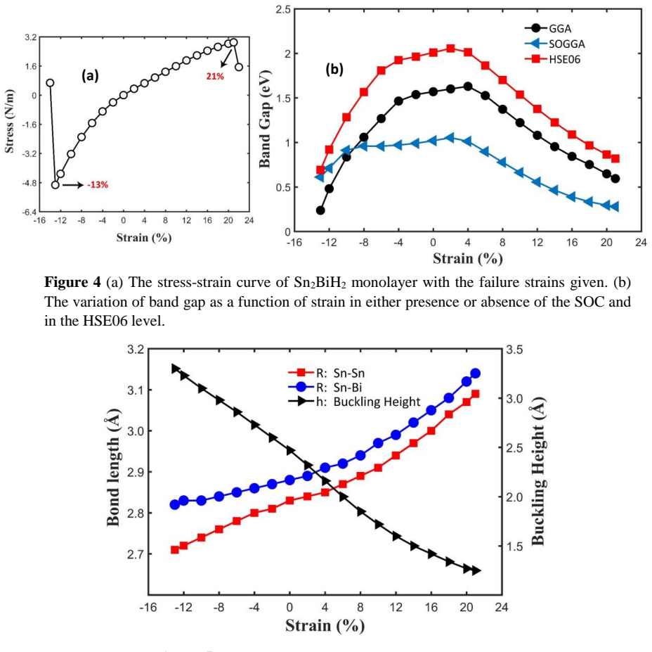
The load-bearing object is the ten-atom rhombic unit cell of Sn2BiH2, a hexagonal Sn network with Bi atoms, passivated by four H atoms. The stabilizing mechanism is electron transfer: population analysis shows H atoms gain charge from Sn and Bi, removing the surplus electrons that make the bare sheet unstable. The tuning mechanism is biaxial strain, which changes the buckling height (2.46 Å at equilibrium, falling under tension and rising under compression) and the Sn-Sn and Sn-Bi bond lengths; these shifts move the valence-band maximum at the Gamma point and the conduction-band minimum near M or K, reducing the gap and eventually making it direct. The paper's argument is carried by comparing generalized-gradient, spin-orbit-coupled, and hybrid-functional band structures under strain, together with phonon dispersion and stress-strain curves.
What would settle it
A more converged phonon calculation using a larger supercell, tighter force thresholds, or an anharmonic treatment that finds the -1.6 $cm^{-1}$ mode remains imaginary, or a search that finds a lower-energy arrangement of hydrogen atoms, would overturn the stability claim. Experimentally, synthesizing free-standing Sn2BiH2 and measuring the band gap by angle-resolved photoemission or optical absorption would test whether the predicted 1.02 to 2.01 eV range and strain tunability are real.
Extended reading notes
Core claim
The paper argues that hydrogen passivation removes the surplus electrons that destabilize isolated Sn2Bi, yielding a free-standing monolayer Sn2BiH2 with an indirect band gap of 1.57 eV at the GGA level, 1.02 eV with spin-orbit coupling, and 2.01 eV in hybrid-functional calculations. The monolayer exhibits flat electron bands near the conduction band and dispersive hole bands near the valence band, and it remains mechanically stable under biaxial strains between -13% and +21%. Under strain, the gap shrinks to about 0.2 eV at high compression and an indirect-to-direct transition appears near +5% tensile strain, which the authors attribute to changes in buckling height and in the strong Sn-Sn and Sn-Bi sigma bonds. The paper further claims that the monolayer is transparent in the infrared and visible range and strongly absorbs and reflects in portions of the ultraviolet, making it a candidate for near-infrared detectors, transistors, sensors, photocatalysis, thermoelectric devices, and flexible optoelectronics.
Load-bearing premise
The result rests on taking the chosen hydrogen-passivated honeycomb configuration as the stable ground state and treating the small imaginary phonon frequency of about -1.6 $cm^{-1}$ near the Gamma point as a numerical artifact rather than a sign of true dynamical instability.
Editorial extensions
If this is right
- The monolayer stays semiconducting under biaxial strain from -13% to +21%, so flexible electronics could exploit large reversible deformation without losing the gap.
- An indirect-to-direct gap transition near +5% strain would improve light emission and absorption, making Sn2BiH2 more useful for optoelectronic devices than a purely indirect semiconductor.
- High hole mobility, with a small effective mass of about -0.26 electron masses at the valence-band maximum, together with strongly localized electrons gives a route to ambipolar or correlated transport in a single monolayer.
- Transparency in the infrared and visible range plus strong ultraviolet response suggests applications as optical filters, transparent conductors, or ultraviolet detectors.
- Band gaps spanning 1.02 to 2.01 eV across the three levels of theory bracket the near-infrared-to-visible range, matching the needs of photodetectors and photocatalysis.
Reading between the lines
- If a more exhaustive search of hydrogen coverages finds another arrangement with comparable or lower energy, the magnitude of the gap and the critical strains would likely shift, but the qualitative picture of a strain-tunable semiconducting hydride may survive.
- The coexistence of flat electron bands and dispersive hole bands suggests that doping or gating Sn2BiH2 could produce strongly correlated electron states in a free-standing monolayer, a possibility the paper mentions only briefly for the substrate-bound sample.
- Because the three computed gaps differ by roughly 1 eV, measuring the optical absorption edge would discriminate which level of theory describes this material, providing a sharp experimental check.
- The strain range from -13% to +21% implies the monolayer could act as a flexible strain sensor, where a simple test would be to measure how its optical absorption edge shifts under bending.
Signed reviews
Editorial analysis
A structured set of objections, weighed in public.
Referee Report
Summary. The manuscript uses DFT (PBE, PBE+SOC, and HSE06) with the SIESTA code to study a hydrogenated free-standing Sn2Bi monolayer (Sn2BiH2) in a ten-atom rhombic honeycomb cell. It reports structural parameters, cohesive energy, phonon dispersion, electronic band structure, effective masses, density of states, electron localization, biaxial strain dependence of the band gap and buckling, electric-field effects, and optical properties from an independent-particle dielectric function. The central claims are that Sn2BiH2 is a dynamically stable semiconductor with an indirect gap (1.57 eV PBE, 1.02 eV PBE+SOC, 2.01 eV HSE06), that the gap can be tuned between about 0.2 and 1.6 eV under biaxial strain from -13% to +21%, with indirect-to-direct transitions, and that the material is transparent in the IR/visible and metallic in parts of the UV.
Significance. If the results hold, the paper offers a potentially useful prediction of a functionalized two-dimensional semiconductor with strain-tunable electronic and optical properties, and it connects to an experimentally realized Sn2Bi/Si(111) system. The work follows standard DFT practice, reports many numerical parameters (cutoff, k-grid, vacuum thickness, tolerances), and provides data from three exchange-correlation treatments plus optical response functions. However, the significance is conditional on the dynamical stability of the proposed structure, which is not convincingly established: the phonon calculation excludes hydrogen-related branches, the one imaginary acoustic mode is dismissed without analysis, and no alternative hydrogenation arrangements are tested. The strain-tuning claims likewise lack stability checks for the strained structures. These gaps prevent the paper from supporting its central 'completely stable and strain-tunable' conclusion as written.
major comments (5)
- [Structural characteristics of Sn2BiH2 monolayer, Fig. 1b and adjacent text] The phonon dispersion is computed and plotted with only the 18 branches of the six Bi/Sn atoms, explicitly excluding branches relevant to H atoms ('Due to the existence of six atoms (Bi, Sn) in the unit cell excluding H atoms, there are 18 phonon branches'). A complete phonon calculation for the ten-atom Sn2BiH2 cell should have 30 branches. Excluding H-related modes is not a harmless simplification: hydrogenation is the proposed stabilization mechanism, and a soft mode involving H motion would directly invalidate the stability claim. The manuscript must either present the full phonon spectrum including all ten atoms or justify why H-related branches can be safely projected out. As it stands, the dynamical stability conclusion is unsupported.
- [Structural characteristics of Sn2BiH2 monolayer, Fig. 1b and adjacent text] The lone imaginary acoustic mode with frequency about -1.6 cm^-1 near the Gamma point is dismissed as 'negligible' without any convergence study or eigenvector analysis. For a 2D crystal, an imaginary acoustic mode near Gamma can indicate a genuine soft mode driving a structural distortion, or it can be a numerical artifact of an insufficient supercell, insufficient k-point sampling, or an acoustic sum-rule violation. The paper reports only a 5x5x1 supercell with a 4x4x1 k-grid and gives no tests with larger supercells or different displacement amplitudes. The 'completely stable' claim in the Introduction and the dynamical stability statement in this section therefore rest on an unverified assertion, which is a load-bearing weakness.
- [Structural characteristics, Fig. 1a and Table 1] The manuscript adopts a specific hydrogenation pattern (four H atoms in the ten-atom rhombic cell) without comparing it with alternative passivation configurations, coverages, or binding sites. Since reference 37 already studied functionalized Sn2Bi nanosheets, the authors should demonstrate that the chosen arrangement is the ground state among plausible candidates, for example by total-energy comparison or by phonon stability checks for the alternatives. Without such a comparison, the structural model underlying every subsequent electronic, strain, and optical result is an unjustified assumption.
- [Electronic characteristics of Sn2BiH2 monolayer under biaxial strain, Fig. 4] The strain-tuning results claim that Sn2BiH2 remains semiconducting and mechanically stable from -13% to +21% strain, and that indirect-direct transitions occur in this range. However, the paper provides no phonon or other dynamical stability calculations for the strained structures; the stress-strain curve alone indicates ideal strength limits, not dynamical stability. A structure can be mechanically stable on the stress-strain curve while being dynamically unstable (imaginary phonons) at a given strain, which would make the reported band gaps and transitions irrelevant for that strain. The authors should either compute phonon spectra at representative strained states or explicitly limit the tuning claims to the range where dynamical stability is verified.
- [Abstract and Introduction] The abstract and the Introduction state that 'the band gap, effective mass, and carrier mobility can be improved and tuned by applying a biaxial strain,' but the manuscript reports only effective masses, not carrier mobilities. No mobility formula, relaxation-time model, or deformation-potential calculation appears anywhere. This is an overclaim that should be corrected by either removing 'carrier mobility' from the claims or adding the missing mobility calculations.
minor comments (5)
- [Computational details, Eq. (1)] The effective mass is written as m* = hbar^2 (d^2E/dk^2)^-1, but the text later reports values like 'm* = -0.26 me' without defining 'me' as the electron mass in that context; please clarify the notation and state the propagation direction for each mass.
- [Throughout] The abbreviation 'SOGGA' is used in Figure 4b and in the text without definition; the paper only defines GGA and SOC. Please define the combined method explicitly.
- [Structural characteristics, Fig. 1b] If the phonon plot intentionally omits H-related branches, the figure caption should state this clearly, and the branch count should be explained in the caption as well as in the text.
- [Optical characteristics, Eq. (4)] The manuscript says the optical response is computed within TDDFT in the independent-particle approximation, but the Kubo-Greenwood formula is a ground-state linear-response expression; please clarify whether excitonic effects are included or neglected, since this affects how the optical spectra should be interpreted.
- [Table 1] The header 'Eg PBE/SOC (eV)' is ambiguous: it appears to list both the PBE gap and the SOC-included gap, but the column headings are not explicit. Please separate the two values with a clearer label.
Circularity Check
No significant circularity: all central predictions are computed ab initio with standard DFT methods, and no fitted parameter or self-cited result is reused as an output.
full rationale
The paper's central claims concern the structural stability, electronic structure, strain response, and optical properties of a hydrogenated Sn2Bi monolayer. These quantities are obtained directly from DFT calculations: geometry optimization with SIESTA, phonon dispersions from a finite-difference dynamical matrix, band structures from GGA/SOC/HSE06, effective masses from band curvature, and optical spectra from the Kubo-Greenwood susceptibility. None of these target results is used as an input to the calculation that produces it. The experimental band gap of 0.87 eV is used only as a comparison value for the computed 1.57 eV gap, not as a fitted parameter. The structural model follows the externally published work of Ding and Wang (ref. 37), which is not authored by the present authors and does not supply any fitted constant on which the present predictions depend. The small imaginary phonon near Gamma is dismissed by assertion rather than by convergence testing, which is a correctness and robustness concern, but it is not a circularity: the negative frequency is reported as a computed outcome and then judged negligible, rather than being removed by construction or imposed by an input. No prediction is statistically forced by a subset fit, no uniqueness theorem is imported from the authors' own prior work, and no known result is merely renamed. The derivation chain is therefore self-contained with respect to the targets it claims to predict, so the appropriate circularity score is 0.
Assumptions & free parameters
assumptions (4)
- domain assumption PBE-GGA and HSE06 exchange-correlation functionals accurately describe the ground-state and band structure of Sn2BiH2.
- domain assumption The Sn2BiH2 structural model with four H atoms passivating the honeycomb Sn2Bi cell is the relevant ground-state configuration.
- ad hoc to paper The small imaginary phonon mode at Gamma (-1.6 cm^-1) is a numerical artifact.
- domain assumption The independent-particle approximation (Kubo-Greenwood formula) is adequate for the optical properties.
Cite this review
Pith. "Pith review of Tuning electronic and optical properties of free-standing Sn2Bi monolayer stabilized by hydrogenation." pith.science (2026). https://pith.science/paper/BZHEF7Y5
@misc{pith2026190803921,
  author       = {Pith},
  title        = {Pith review of: Tuning electronic and optical properties of free-standing Sn2Bi monolayer stabilized by hydrogenation},
  year         = {2026},
  howpublished = {\url{https://pith.science/paper/BZHEF7Y5}},
  note         = {Machine review of arXiv:1908.03921}
}
read the original abstract
In this study, we systematically investigated the structural, mechanical, electronic and optical properties of Sn2Bi monolayer, a sheet experimentally synthesized recently [PRL, 121, 126801 (2018)] which has been hydrogenated (Sn2BiH2) to stabilize free-standing form using density functional theory (DFT). For tuning the band structure and electronic properties, the mechanical strain and electric field are used. Our investigations show that in this free-standing sample, there are electron flat bands and free hole bands like the recently synthesized sample on silicon wafer, which provide the possibility of having strongly localized electrons and free holes with high mobility. Also, the band gap of Sn2BiH2 monolayer has experienced a growth of 80% compared with the experimental sample. The relevant results to strain suggest that the band gap can be properly manipulated by biaxial strain (-13% to +21%) within a range from 0.2 to 1.6 eV. It should be mentioned that the stability and flexibility of the corresponding monolayer under tensile and compressive strain are due to the strong {\sigma} bonds between atoms. We also realized the strain can cause indirect-direct transition in the band gap. Furthermore, our optical findings indicate that the Sn2BiH2 monolayer has almost metallic properties in a specific range of UV spectrum and it is transparent in the IR and visible spectrum of electromagnetic radiation. All these tunable properties and nontrivial features portend that Sn2BiH2 monolayer has great potentials in applications as near-infrared detectors, thermoelectric devices, field-effect transistors, sensors, photocatalysis, energy harvesting, and optoelectronics.
Figures
Reference graph
Works this paper leans on
-
[1]
Sarma SD, Adam S, Hwang EH, Rossi E (2011) Electronic transport in two-dimensional graphene. Reviews of modern physics. 83(2), 407
work page 2011
-
[2]
Bonaccorso F, Colombo L, Yu G, Stoller M, Tozzini V, Ferrari AC, Ruoff RS, Pellegrini V (2015) Graphene, related two-dimensional crystals, and hybrid systems for energy conversion and storage. Science. 347(6217), 1246501. 17
work page 2015
-
[3]
Pan Y, Zhang L, Huang L, Li L, Meng L, Gao M, Huan Q, Lin X, Wang Y, Du S (2014) Construction of 2d atomic crystals on transition metal surfaces: Graphene, silicene, and hafnene. small. 10(11), 2215-2225
work page 2014
-
[4]
Balendhran S, Walia S, Nili H, Sriram S, Bhaskaran M (2015) Elemental analogues of graphene: Silicene, germanene, stanene, and phosphorene. small. 11(6), 640-652
work page 2015
-
[5]
Kaloni TP, Cheng YC, Schwingenschlögl U (2013) Hole doped dirac states in silicene by biaxial tensile strain. Journal of Applied Physics. 113(10), 104305
work page 2013
-
[6]
Zhang S, Xie M, Cai B, Zhang H, Ma Y, Chen Z, Zhu Z, Hu Z, Zeng H (2016) Semiconductor- topological insulator transition of two-dimensional sbas induced by biaxial tensile strain. Physical Review B. 93(24), 245303
work page 2016
-
[7]
Saladukha D, Clavel MB, Murphy-Armando F, Greene-Diniz G, Grüning M, Hudait MK, Ochalski TJ (2018) Direct and indirect band gaps in ge under biaxial tensile strain investigated by photoluminescence and photoreflectance studies. Physical Review B. 97(19), 195304
work page 2018
-
[8]
Computational Materials Science
Liang X, Ng S-P, Ding N, Wu C-ML (2018) Thermal stability of no on ga-doped graphene and effect of external electric field. Computational Materials Science. 151, 214-221
work page 2018
Show all 70 references
-
[9]
Nano letters
Song L, Ci L, Lu H, Sorokin PB, Jin C, Ni J, Kvashnin AG, Kvashnin DG, Lou J, Yakobson BI (2010) Large scale growth and characterization of atomic hexagonal boron nitride layers. Nano letters. 10(8), 3209-3215
2010
-
[10]
Physical review letters
Lin C-L, Arafune R, Kawahara K, Kanno M, Tsukahara N, Minamitani E, Kim Y, Kawai M, Takagi N (2013) Substrate-induced symmetry breaking in silicene. Physical review letters. 110(7), 076801
2013
-
[11]
Nature communications
Jiang S, Butler S, Bianco E, Restrepo OD, Windl W, Goldberger JE (2014) Improving the stability and optical properties of germanane via one-step covalent methyl-termination. Nature communications. 5(10), 3389
2014
-
[12]
Nature materials
Zhu F, Chen W, Xu Y, Gao C, Guan D, Liu C, Qian D, Zhang S, Jia J (2015) Epitaxial growth of two-dimensional stanene. Nature materials. 14(10), 1020
2015
-
[13]
Nano letters
Berweger S, Qiu G, Wang Y-X, Pollard B, Genter KL, Tyrrell-Ead R, Wallis TM, wu wz, Ye PD, Kabos P (2019) Imaging carrier inhomogeneities in ambipolar tellurene field effect transistors. Nano letters
2019
-
[14]
Advanced Materials
Pumera M, Sofer Z (2017) 2D monoelemental arsenene, antimonene, and bismuthene: Beyond black phosphorus. Advanced Materials. 29(21), 1605299
2017
-
[15]
Cantoro M, Heo Y (2019) Field effect transistor including multiple aspect ratio trapping structures
2019
-
[16]
The Astronomical Journal
Simcoe RA, Fűrész G, Sullivan PW, Hellickson T, Malonis A, Kasliwal M, Shectman SA, Kollmeier JA, Moore A (2019) Background-limited imaging in the near infrared with warm ingaas sensors: Applications for time-domain astronomy. The Astronomical Journal. 157(2), 46
2019
-
[17]
Zhou L, Swearer DF, Zhang C, Robatjazi H, Zhao H, Henderson L, Dong L, Christopher P, Carter EA, Nordlander P (2018) Quantifying hot carrier and thermal contributions in plasmonic photocatalysis. Science. 362(6410), 69-72
2018
-
[18]
Chemical Engineering Journal
Du P, Huang X, Yu JS (2018) Facile synthesis of bifunctional eu3+-activated nabif4 red-emitting nanoparticles for simultaneous white light-emitting diodes and field emission displays. Chemical Engineering Journal. 337, 91-100
2018
-
[19]
Journal of Lightwave Technology
Schneider K, Welter P, Baumgartner Y, Hahn H, Czornomaz L, Seidler P (2018) Gallium phosphide-on-silicon dioxide photonic devices. Journal of Lightwave Technology. 36(14), 2994- 3002. 18
2018
-
[20]
Atabaki AH, Moazeni S, Pavanello F, Gevorgyan H, Notaros J, Alloatti L, Wade MT, Sun C, Kruger SA, Meng H (2018) Integrating photonics with silicon nanoelectronics for the next generation of systems on a chip. Nature. 556(7701), 349
2018
-
[21]
Electrochimica Acta
Mortazavi B, Dianat A, Cuniberti G, Rabczuk T (2016) Application of silicene, germanene and stanene for na or li ion storage: A theoretical investigation. Electrochimica Acta. 213, 865-870
2016
-
[22]
Journal of Materials Chemistry A
Shi L, Zhao TS, Xu A, Xu JB (2016) Ab initio prediction of a silicene and graphene heterostructure as an anode material for li-and na-ion batteries. Journal of Materials Chemistry A. 4(42), 16377- 16382
2016
-
[23]
Ab initio study of size and strain effects on the electronic properties of si nanowires
Peng XH, Alizadeh A, Kumar SK, Nayak SK. Ab initio study of size and strain effects on the electronic properties of si nanowires. International Journal of Applied Mechanics. 1(03), 483-499 (2009)
2009
-
[24]
Journal of Physics: Condensed Matter
Peng XH, Alizadeh A, Bhate N, Varanasi KK, Kumar SK, Nayak SK (2007) First-principles investigation of strain effects on the energy gaps in silicon nanoclusters. Journal of Physics: Condensed Matter. 19(26), 266212
2007
-
[25]
Applied Physics Letters
Wei Q, Peng X (2014) Superior mechanical flexibility of phosphorene and few-layer black phosphorus. Applied Physics Letters. 104(25), 251915
2014
-
[26]
Physical Review B
Kamal C, Ezawa M (2015) Arsenene: Two-dimensional buckled and puckered honeycomb arsenic systems. Physical Review B. 91(8), 085423
2015
-
[27]
Nanotechnology
Zeng H, Zhao J, Cheng A-Q, Zhang L, He Z, Chen R-S (2018) Tuning electronic and optical properties of arsenene/c3n van der waals heterostructure by vertical strain and external electric field. Nanotechnology. 29(7), 075201
2018
-
[28]
Chemical reviews
Hochbaum AI, Yang P (2009) Semiconductor nanowires for energy conversion. Chemical reviews. 110(1), 527-546
2009
-
[29]
Physical Chemistry Chemical Physics
Lu P, Wu X, Guo W, Zeng XC (2012) Strain-dependent electronic and magnetic properties of mos 2 monolayer, bilayer, nanoribbons and nanotubes. Physical Chemistry Chemical Physics. 14(37), 13035-13040
2012
-
[30]
Nano letters
Song S, Keum DH, Cho S, Perello D, Kim Y, Lee YH (2015) Room temperature semiconductor– metal transition of mote2 thin films engineered by strain. Nano letters. 16(1), 188-193
2015
-
[31]
Nanotechnology
Manjanath A, Samanta A, Pandey T, Singh AK (2015) Semiconductor to metal transition in bilayer phosphorene under normal compressive strain. Nanotechnology. 26(7), 075701
2015
-
[32]
Diamond and Related Materials
Grishakov KS, Katin KP, Maslov MM (2018) Strain-induced semiconductor-to-metal transitions in c 36-based carbon peapods: Ab initio study. Diamond and Related Materials. 84, 112-118
2018
-
[33]
Physical Chemistry Chemical Physics
Phuc HV, Hieu NN, Hoi BD, Nguyen CV (2018) Interlayer coupling and electric field tunable electronic properties and schottky barrier in a graphene/bilayer-gase van der waals heterostructure. Physical Chemistry Chemical Physics. 20(26), 17899-17908
2018
-
[34]
Nano letters
Ni Z, Liu Q, Tang K, Zheng J, Zhou J, Qin R, Gao Z, Yu D, Lu J (2011) Tunable bandgap in silicene and germanene. Nano letters. 12(1), 113-118
2011
-
[35]
Journal of Materials Chemistry C
Tan C, Yang Q, Meng R, Liang Q, Jiang J, Sun X, Ye H, Chen XP (2016) An alas/germanene heterostructure with tunable electronic and optical properties via external electric field and strain. Journal of Materials Chemistry C. 4(35), 8171-8178
2016
-
[36]
Physical review letters
Gou J, Xia B, Li H, Wang X, Kong L, Cheng P, Li H, Zhang W, Qian T, Ding H (2018) Binary two- dimensional honeycomb lattice with strong spin-orbit coupling and electron-hole asymmetry. Physical review letters. 121(12), 126801. 19
2018
-
[37]
Applied Physics Letters
Ding Y, Wang Y (2019) Stabilizing the isolated sn2bi nanosheet and tailoring its electronic structure by chemical functionalization: A computational study. Applied Physics Letters. 114(7), 073103
2019
-
[38]
Physical Chemistry Chemical Physics
Xu LC, Du A, Kou L (2016) Hydrogenated borophene as a stable two-dimensional Dirac material with an ultrahigh Fermi velocity. Physical Chemistry Chemical Physics. 18(39), 27284-9
2016
-
[39]
Computational Materials Science
Shahrokhi M (2019) Can fluorine and chlorine functionalization stabilize the graphene like borophene?. Computational Materials Science. 156, 56-66
2019
-
[40]
Nanoscale
Mortazavi B, Makaremi M, Shahrokhi M, Raeisi M, Singh CV, Rabczuk T, Pereira LF (2018) Borophene hydride: a stiff 2D material with high thermal conductivity and attractive optical and electronic properties. Nanoscale. 10(8), 3759-68
2018
-
[41]
Applied Materials Today
Mortazavi B, Shahrokhi M, Makaremi M, Rabczuk T (2017) Theoretical realization of Mo2P; a novel stable 2D material with superionic conductivity and attractive optical properties. Applied Materials Today. 9(5), 292-299
2017
-
[42]
Nanotechnology
Mortazavi B, Shahrokhi M, Makaremi M, Rabczuk T (2017) Anisotropic mechanical and optical response and negative Poisson’s ratio in Mo2C nanomembranes revealed by first-principles simulations. Nanotechnology. 28(11), 115705
2017
-
[43]
Phys: Condens
Soler J, Artacho E, Gale J, Garcia A, Junquera J, Ordejon P, and Sanchez-portal D (2002) The SIESTA method for ab initio order-N materials simulation. Phys: Condens. Matter. 14, 2745
2002
-
[44]
Annalen der Physik
Xu Y, Peng B, Zhang H, Shao H, Zhang R, Zhu H (2017) First‐principle calculations of optical properties of monolayer arsenene and antimonene allotropes. Annalen der Physik. 529(4), 1600152
2017
-
[45]
RSC Advances
Liu M-Y, Huang Y, Chen Q-Y, Li Z-Y, Cao C, He Y (2017) Strain and electric field tunable electronic structure of buckled bismuthene. RSC Advances. 7(63), 39546-39555
2017
-
[46]
Physical Review B
Tang P, Chen P, Cao W, Huang H, Cahangirov S, Xian L, Xu Y, Zhang S-C, Duan W, Rubio A (2014) Stable two-dimensional dumbbell stanene: A quantum spin hall insulator. Physical Review B. 90(12), 121408
2014
-
[47]
Journal of Materials Chemistry
Ma Y, Dai Y, Niu C, Huang B (2012) Halogenated two-dimensional germanium: Candidate materials for being of quantum spin hall state. Journal of Materials Chemistry. 22(25), 12587-12591
2012
-
[48]
Angewandte Chemie
Zhang S, Xie M, Li F, Yan Z, Li Y, Kan E, Liu W, Chen Z, Zeng H (2016) Semiconducting group 15 monolayers: A broad range of band gaps and high carrier mobilities. Angewandte Chemie. 128(5), 1698-1701
2016
-
[49]
Effect of external strain on electronic structure of stanene
Modarresi M, Kakoee A, Mogulkoc Y, Roknabadi MR (2015). Effect of external strain on electronic structure of stanene. Computational Materials Science. 101(5), 164-167
2015
-
[50]
Journal of inorganic and nuclear chemistry
Allred AL (1961) Electronegativity values from thermochemical data. Journal of inorganic and nuclear chemistry. 17(3-4), 215-221
1961
-
[51]
Phonon instability and ideal strength of silicene under tension
Yang C, Yu Z, Lu P, Liu Y, Ye H, Gao T (2014). Phonon instability and ideal strength of silicene under tension. Computational Materials Science. 95(2), 420-428
2014
-
[52]
New Journal of Physics
Wang H, Li Q, Gao Y, Miao F, Zhou X-F, Wan XG (2016) Strain effects on borophene: Ideal strength, negative possion’s ratio and phonon instability. New Journal of Physics. 18(7), 073016
2016
-
[53]
Physica E: Low- dimensional Systems and Nanostructures
Mortazavi B, Rahaman O, Makaremi M, Dianat A, Cuniberti G, Rabczuk T (2017) First-principles investigation of mechanical properties of silicene, germanene and stanene. Physica E: Low- dimensional Systems and Nanostructures. 87, 228-232
2017
-
[54]
ACS applied materials & interfaces
Wang G, Pandey R, Karna SP (2015) Atomically thin group v elemental films: Theoretical investigations of antimonene allotropes. ACS applied materials & interfaces. 7(21), 11490-11496
2015
-
[55]
Nature communications
Akinwande D, Petrone N, Hone J (2014) Two-dimensional flexible nanoelectronics. Nature communications. 5(5), 5678. 20
2014
-
[56]
Physical Review B
Liu F, Ming P, Li J (2007) Ab initio calculation of ideal strength and phonon instability of graphene under tension. Physical Review B. 76(6), 064120
2007
-
[57]
Superlattices and Microstructures
Cao H, Yu Z, Lu P (2015) Electronic properties of monolayer and bilayer arsenene under in-plain biaxial strains. Superlattices and Microstructures. 86, 501-507
2015
-
[58]
Physical Review B
Peng X, Wei Q, Copple A (2014) Strain-engineered direct-indirect band gap transition and its mechanism in two-dimensional phosphorene. Physical Review B. 90(8), 085402
2014
-
[59]
Journal of Physics D: Applied Physics
Wang Y-p, Zhang C-w, Ji W-x, Zhang R-w, Li P, Wang P-j, Ren M-j, Chen X-l, Yuan M (2016) Tunable quantum spin hall effect via strain in two-dimensional arsenene monolayer. Journal of Physics D: Applied Physics. 49(5), 055305
2016
-
[60]
Solid State Communications
Li W, Wang T, Dai X, Wang X, Zhai C, Ma Y, Chang S (2016) Bandgap engineering of different stacking ws2 bilayer under an external electric field. Solid State Communications. 225(10), 32-37
2016
-
[61]
Nanoscale
Lu N, Guo H, Li L, Dai J, Wang L, Mei W-N, Wu X, Zeng XC (2014) Mos 2/mx 2 heterobilayers: Bandgap engineering via tensile strain or external electrical field. Nanoscale. 6(5), 2879-2886
2014
-
[62]
Journal of Materials Chemistry C
Liu G, Luo WW, Wang X, Lei XL, Xu B, Ouyang CY, Liu SB (2018) Tuning the electronic properties of germanene by molecular adsorption and under an external electric field. Journal of Materials Chemistry C. 6(22), 5937-5948
2018
-
[63]
Journal of Materials Chemistry C
Chen X, Yang Q, Meng R, Jiang J, Liang Q, Tan C, Sun X (2016) The electronic and optical properties of novel germanene and antimonene heterostructures. Journal of Materials Chemistry C. 4(23), 5434-5441
2016
-
[64]
Physical Chemistry Chemical Physics
Chen X, Meng R, Jiang J, Liang Q, Yang Q, Tan C, Sun X, Zhang S, Ren T (2016) Electronic structure and optical properties of graphene/stanene heterobilayer. Physical Chemistry Chemical Physics. 18(24), 16302-16309
2016
-
[65]
Physical Review B
Kecik D, Durgun E, Ciraci S (2016) Optical properties of single-layer and bilayer arsenene phases. Physical Review B. 94(20), 205410
2016
-
[66]
Harrison WA (1980) Solid state theory: Courier Corporation
1980
-
[67]
Physica E: Low- dimensional Systems and Nanostructures
Mohan B, Kumar A, Ahluwalia PK (2012) A first principle study of interband transitions and electron energy loss in mono and bilayer graphene: Effect of external electric field. Physica E: Low- dimensional Systems and Nanostructures. 44(7-8), 1670-1674
2012
-
[68]
Surface Science
Kuzumaki T, Shirasawa T, Mizuno S, Ueno N, Tochihara H, Sakamoto K (2010) Re-investigation of the Bi-induced Si (111)-(3× 3) surfaces by low-energy electron diffraction. Surface Science. 604(11), 1044-1048
2010
-
[69]
Nicolosi V, Chhowalla M, Kanatzidis G, Strano S, Coleman N (2013) Liquid exfoliation of layered materials. Science. 340(6139), 1226419
2013
-
[70]
Nature communications 7(13), 13261-13267
Son J, Soogil L, Sang J, Byung C, Han L, Sanghoon K, Jae H, Byung H, and Jongill H (2016) Hydrogenated monolayer graphene with reversible and tunable wide band gap and its field-effect transistor. Nature communications 7(13), 13261-13267
2016
Reviewed August 14, 2026 · model on record in the stance chip above.
Discussion (0). Continue with ORCID to comment.