REVIEW 4 major objections 5 minor 53 references
Improving the lifetime of aluminum-based superconducting qubits through atomic layer etching and deposition
T0 review · 4 major / 5 minor · reviewed 2026-08-15 · deepseek-v4-flash
Pith's one-line read A post-fabrication dry etch-and-coat treatment doubles the energy-relaxation time of aluminum superconducting qubits to a median of 196 microseconds.
desk verdict A well-characterized post-fabrication surface treatment for Al qubits with a plausible two-fold TLS loss reduction, but the thermal-budget control is too thin to fully separate the chemistry from the anneal. read the letter →
The pith
A machine-rendered reading of the paper's core claim, the machinery that carries it, and where it could break.
The reading
What carries the argument
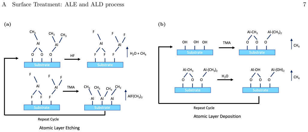
The load-bearing mechanism is the ALE+ALD process itself: self-limiting half-cycles of HF-pyridine and trimethylaluminum etch Al2O3 at about 0.5 Å/cycle, and in-situ TMA/H2O ALD regrows about 1 nm of stoichiometric Al2O3 at 1 Å/cycle, all at 300 °C. This replaces the lossy native oxide with a clean cap while the thermal step weakens PMMA adhesion, allowing the etchant to remove resist residues from aluminum and silicon alike. The argument works by showing that these chemical changes track the measured reduction in TLS loss.
What would settle it
Measure the single-photon TLS loss tangent on junction-free resonators after the full ALE+ALD recipe, after an annealed-only control, and with XPS assay of residual fluorine: if the annealed-only chip reproduces the twofold loss reduction, or if residual fluorine correlates with the loss change, the surface-TLS attribution would collapse.
Extended reading notes
Core claim
The authors claim that thermal ALE with alternating trimethylaluminum and HF-pyridine, followed in situ by ALD of a ~1-nm stoichiometric Al2O3 cap, removes the oxygen-rich native oxide and polymeric fabrication residues from all exposed aluminum and silicon surfaces of a finished device, reducing the TLS defect density that dominates single-photon loss. The direct evidence is a roughly 50% drop in $\delta_{\mathrm{TLS}}$ for treated coplanar-waveguide resonators and a matching twofold rise in transmon $Q$ and $T_1$, with no such gain from a 300 °C anneal alone. Surface characterization (XPS, PiFM, TEM-EELS) shows thinner, more stoichiometric alumina and greatly reduced PMMA contamination, which the authors tie to the loss reduction; they are explicit that the study correlates material quality with device performance rather than isolating every contribution.
Load-bearing premise
The causal claim assumes that the lifetime gain comes from fewer surface TLS defects in the capacitor, not from the treatment's simultaneous effect on the Josephson junction (it shifts qubit frequency by 500–800 MHz), from the 300 °C anneal, or from unmeasured etching residues such as fluorine.
Editorial extensions
If this is right
- Median energy-relaxation time of treated Al-on-Si transmons rises to $T_1 = 196 \pm 22~\mu\mathrm{s}$, with median $Q = 3.69 \pm 0.42 \times 10^6$; some devices exceed $9 \times 10^6$.
- The same treatment halves TLS loss in junction-free coplanar waveguide resonators across 5.2–6.2 GHz, indicating the effect is not specific to qubit junctions.
- Improvements persist for at least 8–9 months after treatment, so the clean surface does not quickly re-oxidize or re-contaminate in storage.
- Because the treatment applies to fully fabricated devices and covers sidewalls as well as top surfaces, it extends beyond capping strategies that leave exposed superconductor sidewalls lossy.
- The process is compatible with aluminum, unlike common wet oxide etchants, so it can be applied where buffered oxide etchant or tri-acid treatments would damage the metal.
Reading between the lines
- If the surface-TLS interpretation is right, extending the etch chemistry to also strip native silicon oxide from exposed substrate areas could push the substrate-air interface to even lower loss.
- The observed anticorrelation between qubit $Q$ and the treatment-induced frequency shift suggests that if the anneal's junction shift could be suppressed, treated devices would show larger gains at high frequencies.
- The 1-nm ALD cap is the new surface that sees the electromagnetic field; testing alternative low-loss ALD dielectrics in the same process flow would directly show whether the cap's own TLS contribution can be lowered further.
Signed reviews
Editorial analysis
A structured set of objections, weighed in public.
Referee Report
Summary. The paper reports a dry post-fabrication surface treatment for aluminum-on-silicon superconducting circuits, combining atomic layer etching (ALE) of the native aluminum oxide with in situ atomic layer deposition (ALD) of a thin Al2O3 cap. The authors measure microwave resonator internal loss and planar transmon T1/Q before and after the treatment, reporting a two-fold reduction in TLS-associated loss in resonators and a comparable improvement in transmons, with median Q = 3.69 ± 0.42 × 10^6 and T1 = 196 ± 22 μs after treatment. They support the interpretation with surface characterization using XPS, PiFM, and TEM-EELS, showing removal of PMMA contamination, reduction of oxyhydroxide species, and a thinner, more stoichiometric surface oxide. A single annealed-only transmon chip is used as a thermal-budget control, and the authors acknowledge that junction properties change during the process.
Significance. If the central claim holds, this is a practically valuable result: a scalable, conformal, Al-compatible surface treatment applied at the end of the fabrication flow that more than doubles transmon coherence, with demonstrated stability over months. The surface analysis is unusually thorough for a device-focused paper, and the direct before/after comparison on the same transmon chips is a strong experimental design. The paper also makes a falsifiable prediction—that surface TLS density is reduced—which is grounded in standard high/low-power loss extraction rather than fitted to the outcome. The main risk, as the authors partly acknowledge, is that the 300 °C thermal budget itself produces some of the chemical changes and device shifts, and the controls presently are insufficient to fully separate the ALE/ALD chemistry from the anneal.
major comments (4)
- [§II.A and Methods IV.C] The resonator result lacks an annealed-only control group. The central claim of a two-fold reduction in δ_TLS (Eq. 1) is attributed to the ALE+ALD chemistry, but the process is performed at 300 °C, and the XPS data in §II.C show that annealing alone removes Al-O-OH and reduces O=C-O carbon. Without a resonator chip subjected only to the same thermal budget, the observed reduction in δ_TLS cannot be separated from the anneal's chemical effects. The authors should either add an annealed-only resonator cohort or explicitly weaken the causal claim to 'treatment, including its thermal budget,' and discuss what the resonator data do and do not establish.
- [§II.B and SI Sections II–III] The transmon attribution rests on a single annealed-only chip, which is underpowered for the variance in T1/Q distributions shown in Figure 2. Moreover, the treatment shifts f01 upward by 500–800 MHz (SI Section III) and the paper states in §II.D that 'changes in the junction also occur during the ALE/ALD process' with unexplained resistance changes. The Purcell curves in SI Section II are modeled, not measured corrections, and the reported median Q and T1 are not compensated for the frequency-dependent Purcell contribution. The causal step from 'ALE+ALD treatment improves T1/Q' to 'surface TLS density in the capacitor is reduced' is therefore load-bearing and not fully tested. The authors should present a quantitative estimate of the maximum Purcell contribution to the reported improvement, or measure TLS density directly (e.g., via temperature-dependent loss or coherent TLS spectroscopy) on treated versus annealed-only devices.
- [§II.C and Methods IV.D] Fluorine incorporation is not assayed, although the ALE process uses HF-pyridine and the proposed mechanism in Eq. (2) forms AlF3 as a surface intermediate. The XPS measurements (Figures 3 and SI-5 through SI-7) do not include a F 1s spectrum, and the paper does not discuss fluorine residues as a possible loss source or as a marker of incomplete ALE. Given that the treatment is claimed to produce a clean, stoichiometric Al2O3 surface, the absence of any fluorine assay leaves an important gap in the surface-chemistry evidence chain. The authors should provide F 1s XPS data or another direct measurement of residual fluorine on treated surfaces.
- [§II.A and Methods IV.C] The resonator statistics are reported only as 'three resonators on two devices' for each group, with no per-device error bars on the derived δ_TLS values or on the factor-of-two reduction. Figure 1 shows three representative pairs, but the reader cannot assess the scatter or significance of the improvement. The authors should report all paired values, the uncertainty on each δ_TLS extraction (including the HP/LP fitting errors), and a statistical test of the difference between treated and untreated groups.
minor comments (5)
- [§II.B, Eq. (2)] The definition of the effective quality factor is unclear as typeset: 'Q = 2π f01 T1 4' appears to contain a spurious superscript or missing denominator. Please state explicitly whether Q = 2π f01 T1 or Q = 2π f01 T1 / 4, and use a consistent notation in the abstract, main text, and SI.
- [§II.B, Figure 2(c)] The e-PDF and e-CDF are described as empirical distributions, but the reported medians and MADs presumably come from a bootstrap or resampling procedure. Please state the resampling method and the number of samples used for the error bars.
- [§IV.C, 'three resonators on two devices'] The main text says three resonators on two devices for both untreated and treated samples, but the caption of Figure 1 says 'three representative resonators.' Please clarify whether these are the same three resonators, and whether the two devices each contribute multiple resonators.
- [§II.C, PiFM discussion] The statement that residual PMMA forms a continuous layer of at least ~2 nm thickness on the untreated surface is supported by a shielding test described only loosely in the text. Please provide the test details or a reference for the thickness estimate.
- [§II.D] The sentence 'While our study does not disentangle the individual contributions of polymeric residue removal and Al oxide layer modification' is an important limitation that should be placed earlier in the paper, ideally in the abstract or introduction, so that readers do not overinterpret the causal mechanism.
Circularity Check
No significant circularity: the two-fold improvement is a directly measured experimental result, not a quantity fitted or defined into existence.
full rationale
The paper's central claim—a two-fold reduction in TLS loss and increased Q and T1 after ALE+ALD treatment—is a directly measured experimental comparison, not a derived quantity that reduces to its inputs. Resonator TLS loss is extracted with the standard power-saturation subtraction delta_TLS = 1/Q_i,LP - 1/Q_i,HP (Eq. 1), and transmon Q is computed from measured T1 and f01 via Q = 2*pi*f01*T1; neither quantity is fitted to produce the improvement. The surface-chemistry changes are characterized independently by XPS, PiFM, and TEM-EELS, and the paper explicitly presents the connection as correlation rather than derivation: 'While our study does not disentangle the individual contributions of polymeric residue removal and Al oxide layer modification, it establishes a direct correlation between improved material quality at the MA and SA interfaces and increased resonator Q and transmon T1.' The only AWS-authored citations (Refs. 20, 50, 51) concern resonator measurement methods, fitting procedures, and cryogenic setup; they establish how data were taken and analyzed, and none contains or presupposes the observed improvement. The single annealed-only transmon chip is an experimental-control limitation on attributing the gain specifically to surface TLS density rather than thermal or junction effects, but that is an attribution concern, not a definitional or fitting circularity. Therefore no load-bearing step reduces to its own inputs.
Assumptions & free parameters
assumptions (6)
- domain assumption The low-power/high-power resonator loss difference (delta_TLS = 1/Q_LP - 1/Q_HP) isolates TLS absorption from other loss channels.
- domain assumption TLS density is approximately frequency-independent over 2.2-4.4 GHz, so Q = 2*pi*f01*T1 is a valid frequency-independent figure of merit (standard tunneling model).
- ad hoc to paper The ALE process with TMA/HF-pyridine selectively removes Al2O3, including on device sidewalls, without removing the exposed Al metal or Si and without leaving fluorine residues that affect loss.
- domain assumption Annealing alone at 300 C in the ALD chamber is an adequate control for the thermal component of the ALE+ALD process.
- domain assumption XPS-derived oxide thickness using fixed IMFPs (lambda0=28 A, lambdam=26 A, Nm:N0=1.5) and TEM-EELS measurements give representative values for the device surfaces.
- ad hoc to paper The observed improvement in transmon T1/Q is not primarily caused by the treatment-induced change in the Josephson junction (500-800 MHz upward f01 shift) and the resulting Purcell loss variation.
Cite this review
Pith. "Pith review of Improving the lifetime of aluminum-based superconducting qubits through atomic layer etching and deposition." pith.science (2026). https://pith.science/paper/7TNVETZQ
@misc{pith2026250617474,
  author       = {Pith},
  title        = {Pith review of: Improving the lifetime of aluminum-based superconducting qubits through atomic layer etching and deposition},
  year         = {2026},
  howpublished = {\url{https://pith.science/paper/7TNVETZQ}},
  note         = {Machine review of arXiv:2506.17474}
}
abstract
We present a dry surface treatment combining atomic layer etching and deposition (ALE and ALD) to mitigate dielectric loss in fully fabricated superconducting quantum devices formed from aluminum thin films on silicon. The treatment, performed as a final processing step prior to device packaging, starts by conformally removing the native metal oxide and fabrication residues from the exposed surfaces through ALE before \textit{in situ} encapsulating the metal surfaces with a thin dielectric layer using ALD. We measure a two-fold reduction in loss attributed to two-level system (TLS) absorption in treated aluminum-based resonators and planar transmon qubits. Treated transmons with compact capacitor plates and gaps achieve median $Q$ and $T_1$ values of $3.69 \pm 0.42 \times 10^6$ and $196 \pm 22$~$\mu$s, respectively. These improvements were found to be sustained over several months. We discuss how the combination of ALE and ALD reverses fabrication-induced surface damages to significantly and durably improve device performance via a reduction of the TLS defect density in the capacitive elements.
Figures


Figures from the paper (3 more)


Reference graph
Works this paper leans on
-
[1]
G. Wendin, ``Quantum information processing with superconducting circuits: a review,'' Reports on Progress in Physics , vol. 80, no. 10, p. 106001, 2017
work page 2017
- [2]
-
[3]
C. Wang, C. Axline, Y. Y. Gao, T. Brecht, Y. Chu, L. Frunzio, M. H. Devoret, and R. J. Schoelkopf, ``Surface participation and dielectric loss in superconducting qubits,'' Applied Physics Letters , vol. 107, no. 16, 2015
work page 2015
-
[4]
J. M. Gambetta, C. E. Murray, Y.-K.-K. Fung, D. T. McClure, O. Dial, W. Shanks, J. W. Sleight, and M. Steffen, ``Investigating surface loss effects in superconducting transmon qubits,'' IEEE Transactions on Applied Superconductivity , vol. 27, no. 1, pp. 1--5, 2016
work page 2016
-
[5]
M. D. Reed, B. R. Johnson, A. A. Houck, L. DiCarlo, J. M. Chow, D. I. Schuster, L. Frunzio, and R. J. Schoelkopf, ``Fast reset and suppressing spontaneous emission of a superconducting qubit,'' Applied Physics Letters , vol. 96, no. 20, 2010
work page 2010
-
[6]
E. Jeffrey, D. Sank, J. Y. Mutus, T. C. White, J. Kelly, R. Barends, Y. Chen, Z. Chen, B. Chiaro, A. Dunsworth, et al. , ``Fast accurate state measurement with superconducting qubits,'' Physical review letters , vol. 112, no. 19, p. 190504, 2014
work page 2014
-
[7]
C. E. Murray, ``Material matters in superconducting qubits,'' Materials Science and Engineering: R: Reports , vol. 146, p. 100646, 2021
work page 2021
-
[8]
A. P. M. Place, L. V. H. Rodgers, P. Mundada, B. M. Smitham, M. Fitzpatrick, Z. Leng, A. Premkumar, J. Bryon, A. Vrajitoarea, S. Sussman, et al. , ``New material platform for superconducting transmon qubits with coherence times exceeding 0.3 milliseconds,'' Nature communications , vol. 12, no. 1, p. 1779, 2021
work page 2021
Show all 53 references
-
[9]
M. P. Bland, F. Bahrami, J. G. C. Martinez, P. H. Prestegaard, B. M. Smitham, A. Joshi, E. Hedrick, A. Pakpour-Tabrizi, S. Kumar, A. Jindal, et al. , ``2 D transmons with lifetimes and coherence times exceeding 1 millisecond,'' arXiv preprint arXiv:2503.14798 , 2025
2025 arXiv
-
[10]
Woods, G
W. Woods, G. Calusine, A. Melville, A. Sevi, E. Golden, D. K. Kim, D. Rosenberg, J. L. Yoder, and W. D. Oliver, ``Determining interface dielectric losses in superconducting coplanar-waveguide resonators,'' Physical Review Applied , vol. 12, no. 1, p. 014012, 2019
2019
-
[11]
M. V. P. Alto \'e , A. Banerjee, C. Berk, A. Hajr, A. Schwartzberg, C. Song, M. Alghadeer, S. Aloni, M. J. Elowson, J. M. Kreikebaum, et al. , ``Localization and mitigation of loss in niobium superconducting circuits,'' PRX Quantum , vol. 3, no. 2, p. 020312, 2022
2022
-
[12]
K. D. Crowley, R. A. McLellan, A. Dutta, N. Shumiya, A. P. M. Place, X. H. Le, Y. Gang, T. Madhavan, M. P. Bland, R. Chang, et al. , ``Disentangling losses in tantalum superconducting circuits,'' Physical Review X , vol. 13, no. 4, p. 041005, 2023
2023
-
[13]
C. J. Kopas, D. P. Goronzy, T. Pham, C. G. Torres Castanedo, M. Cheng, R. Cochrane, P. Nast, E. Lachman, N. Z. Zhelev, A. Valli \`e res, et al. , ``Enhanced superconducting qubit performance through ammonium fluoride etch,'' Materials for Quantum Technology , 2024
2024
-
[14]
D. P. Lozano, M. Mongillo, X. Piao, S. Couet, D. Wan, Y. Canvel, A. M. Vadiraj, T. Ivanov, J. Verjauw, R. Acharya, et al. , ``Low-loss -tantalum coplanar waveguide resonators on silicon wafers: fabrication, characterization and surface modification,'' Materials for Quantum Tec...
2024
-
[15]
C. Zhou, J. Mun, J. Yao, A. k. Anbalagan, M. D. Hossain, R. A. McLellan, R. Li, K. Kisslinger, G. Li, X. Tong, et al. , ``Ultrathin magnesium-based coating as an efficient oxygen barrier for superconducting circuit materials,'' Advanced Materials , vol. 36, no. 18, p. 2310280, 2024
2024
-
[16]
M. Bal, A. A. Murthy, S. Zhu, F. Crisa, X. You, Z. Huang, T. Roy, J. Lee, D. v. Zanten, R. Pilipenko, et al. , ``Systematic improvements in transmon qubit coherence enabled by niobium surface encapsulation,'' npj Quantum Information , vol. 10, no. 1, p. 43, 2024
2024
-
[17]
S. K. Karuppannan, D. Huang, N. M. Kommanaboina, K. Anil, G. Yan, D. V. M. Repaka, Y. Zhang, K. E. J. Goh, W. S. Kai, N. L. C. Beng, et al. , ``Improved interface of niobium superconducting resonator with ruthenium as a capping layer,'' ACS Applied Electronic Materials , 2024
2024
-
[18]
R. D. Chang, N. Shumiya, R. A. McLellan, Y. Zhang, M. P. Bland, F. Bahrami, J. Mun, C. Zhou, K. Kisslinger, G. Cheng, et al. , ``Eliminating surface oxides of superconducting circuits with noble metal encapsulation,'' Physical review letters , vol. 134, no. 9, p. 097001, 2025
2025
-
[19]
C. R. H. McRae, H. Wang, J. Gao, M. R. Vissers, T. Brecht, A. Dunsworth, D. P. Pappas, and J. Mutus, ``Materials loss measurements using superconducting microwave resonators,'' Review of Scientific Instruments , vol. 91, no. 9, 2020
2020
-
[20]
Marcaud, D
G. Marcaud, D. Perello, C. Chen, E. Umbarkar, C. Weiland, J. Gao, S. Diez, V. Ly, N. Mahuli, N. D'Souza, et al. , ``Low-loss superconducting resonators fabricated from tantalum films grown at room temperature,'' arXiv preprint arXiv:2501.09885 , 2025
2025 arXiv
-
[21]
Q.-M. Chen, M. Pfeiffer, M. Partanen, F. Fesquet, K. E. Honasoge, F. Kronowetter, Y. Nojiri, M. Renger, K. G. Fedorov, A. Marx, et al. , ``Scattering coefficients of superconducting microwave resonators. i. transfer matrix approach,'' Physical Review B , vol. 106, no. 21, p. 2...
2022
-
[22]
P. G. Baity, C. Maclean, V. Seferai, J. Bronstein, Y. Shu, T. Hemakumara, and M. Weides, ``Circle fit optimization for resonator quality factor measurements: Point redistribution for maximal accuracy,'' Physical Review Research , vol. 6, no. 1, p. 013329, 2024
2024
-
[23]
Calusine, A
G. Calusine, A. Melville, W. Woods, R. Das, C. Stull, V. Bolkhovsky, D. Braje, D. Hover, D. K. Kim, X. Miloshi, et al. , ``Analysis and mitigation of interface losses in trenched superconducting coplanar waveguide resonators,'' Applied Physics Letters , vol. 112, no. 6, 2018
2018
-
[24]
Barends, J
R. Barends, J. Kelly, A. Megrant, D. Sank, E. Jeffrey, Y. Chen, Y. Yin, B. Chiaro, J. Mutus, C. Neill, et al. , ``Coherent josephson qubit suitable for scalable quantum integrated circuits,'' Physical review letters , vol. 111, no. 8, p. 080502, 2013
2013
-
[25]
P. V. Klimov, J. Kelly, Z. Chen, M. Neeley, A. Megrant, B. Burkett, R. Barends, K. Arya, B. Chiaro, Y. Chen, et al. , ``Fluctuations of energy-relaxation times in superconducting qubits,'' Physical review letters , vol. 121, no. 9, p. 090502, 2018
2018
-
[26]
Anomalies
C. C Yu and H. M. Carruzzo, ``Two-level systems and the tunneling model: A critical view,'' Low-temperature Thermal And Vibrational Properties Of Disordered Solids: A Half-century Of Universal" Anomalies" Of Glasses , p. 113, 2022
2022
-
[27]
Y. Lee, J. W. DuMont, and S. M. George, ``Trimethylaluminum as the metal precursor for the atomic layer etching of A l _ 2 O _ 3 using sequential, self-limiting thermal reactions,'' Chemistry of Materials , vol. 28, no. 9, pp. 2994--3003, 2016
2016
-
[28]
R. L. Puurunen, ``Surface chemistry of atomic layer deposition: A case study for the trimethylaluminum/water process,'' Journal of applied physics , vol. 97, no. 12, 2005
2005
-
[29]
Prasanna, G
S. Prasanna, G. Krishnendu, S. Shalini, P. Biji, G. M. Rao, S. Jayakumar, and R. Balasundaraprabhu, ``Composition, structure and electrical properties of DC reactive magnetron sputtered A l _ 2 O _ 3 thin films,'' Materials science in semiconductor processing , vol. 16, no. 3,...
2013
-
[30]
Reddy, P
N. Reddy, P. Bera, V. R. Reddy, N. Sridhara, A. Dey, C. Anandan, and A. K. Sharma, `` XPS study of sputtered alumina thin films,'' Ceramics International , vol. 40, no. 7, pp. 11099--11107, 2014
2014
-
[31]
G. A. Mengesha, J. P. Chu, B.-S. Lou, and J.-W. Lee, ``Corrosion performance of plasma electrolytic oxidation grown oxide coating on pure aluminum: effect of borax concentration,'' Journal of Materials Research and Technology , vol. 9, no. 4, pp. 8766--8779, 2020
2020
-
[32]
Nguyen, T
L. Nguyen, T. Hashimoto, D. N. Zakharov, E. A. Stach, A. P. Rooney, B. Berkels, G. E. Thompson, S. J. Haigh, and T. L. Burnett, ``Atomic-scale insights into the oxidation of aluminum,'' ACS applied materials & interfaces , vol. 10, no. 3, pp. 2230--2235, 2018
2018
-
[33]
G. Duan, C. Zhang, A. Li, X. Yang, L. Lu, and X. Wang, ``Preparation and characterization of mesoporous zirconia made by using a poly (methyl methacrylate) template,'' Nanoscale research letters , vol. 3, pp. 118--122, 2008
2008
-
[34]
S. B. Aziz, O. G. Abdullah, M. Brza, A. K. Azawy, and D. A. Tahir, ``Effect of carbon nano-dots ( CND s) on structural and optical properties of PMMA polymer composite,'' Results in Physics , vol. 15, p. 102776, 2019
2019
-
[35]
D. N. Goldstein, J. A. McCormick, and S. M. George, ``Al _ 2 O _ 3 atomic layer deposition with trimethylaluminum and ozone studied by in situ transmission FTIR spectroscopy and quadrupole mass spectrometry,'' The Journal of Physical Chemistry C , vol. 112, no. 49, pp. 19530--...
2008
-
[36]
Vemuri, S
V. Vemuri, S. W. King, W. A. Lanford, J. T. Gaskins, P. E. Hopkins, J. Van Derslice, H. Li, and N. C. Strandwitz, ``Comprehensive study of the chemical, physical, and structural evolution of molecular layer deposited alucone films during thermal processing,'' Chemistry of Mate...
1916
-
[37]
Kashiwagi, A
T. Kashiwagi, A. Inabi, and A. Hamins, ``Behavior of primary radicals during thermal degradation of poly (methyl methacrylate),'' Polymer Degradation and Stability , vol. 26, no. 2, pp. 161--184, 1989
1989
-
[38]
L. E. Manring, ``Thermal degradation of poly (methyl methacrylate). 4. random side-group scission,'' Macromolecules , vol. 24, no. 11, pp. 3304--3309, 1991
1991
-
[39]
H. A. Al-Abadleh and V. Grassian, `` FT - IR study of water adsorption on aluminum oxide surfaces,'' Langmuir , vol. 19, no. 2, pp. 341--347, 2003
2003
-
[40]
Y. Lee, J. W. DuMont, A. S. Cavanagh, and S. M. George, ``Atomic layer deposition of A l F _ 3 using trimethylaluminum and hydrogen fluoride,'' The Journal of Physical Chemistry C , vol. 119, no. 25, pp. 14185--14194, 2015
2015
-
[41]
J. W. DuMont and S. M. George, ``Competition between A l _ 2 O _ 3 atomic layer etching and A l F _ 3 atomic layer deposition using sequential exposures of trimethylaluminum and hydrogen fluoride,'' The Journal of Chemical Physics , vol. 146, no. 5, 2017
2017
-
[42]
G. P. Gakis, H. Vergnes, F. Cristiano, Y. Tison, C. Vahlas, B. Caussat, A. G. Boudouvis, and E. Scheid, `` I n situ N _ 2 - NH _ 3 plasma pre-treatment of silicon substrate enhances the initial growth and restricts the substrate oxidation during alumina ALD ,'' Journal of Appl...
2019
-
[43]
W. Xu, R. J. Gasvoda, P. C. Lemaire, K. Sharma, D. M. Hausmann, and S. Agarwal, ``Area-selective atomic layer deposition of A l _ 2 O _ 3 on S i N _ x with S i O _ 2 as the nongrowth surface,'' Journal of Vacuum Science & Technology A , vol. 40, no. 1, 2022
2022
-
[44]
W. Xu, P. C. Lemaire, K. Sharma, D. M. Hausmann, and S. Agarwal, ``Extending growth inhibition during area-selective atomic layer deposition of A l _ 2 O _ 3 on aminosilane-functionalized S i O _ 2 ,'' Chemical Communications , vol. 58, no. 46, pp. 6650--6652, 2022
2022
-
[45]
Papirer, J.-M
E. Papirer, J.-M. Perrin, G. Nanse, and P. Fioux, ``Adsorption of poly (methylmethacrylate) on an alumina: evidence of formation of surface carboxylate bonds,'' European polymer journal , vol. 30, no. 8, pp. 985--991, 1994
1994
-
[46]
J. F. Watts, S. R. Leadley, J. E. Castle, and C. J. Blomfield, ``Adsorption of PMMA on oxidized A l and S i substrates: An investigation by high-resolution X -ray photoelectron spectroscopy,'' Langmuir , vol. 16, no. 5, pp. 2292--2300, 2000
2000
-
[47]
Ferriol, A
M. Ferriol, A. Gentilhomme, M. Cochez, N. Oget, and J. L. Mieloszynski, ``Thermal degradation of poly (methyl methacrylate)( PMMA ): modelling of DTG and TG curves,'' Polymer degradation and stability , vol. 79, no. 2, pp. 271--281, 2003
2003
-
[48]
Almajhadi and H
M. Almajhadi and H. K. Wickramasinghe, ``Contrast and imaging performance in photo induced force microscopy,'' Optics Express , vol. 25, no. 22, pp. 26923--26938, 2017
2017
-
[49]
R. A. McLellan, A. Dutta, C. Zhou, Y. Jia, C. Weiland, X. Gui, A. P. M. Place, K. D. Crowley, X. H. Le, T. Madhavan, et al. , ``Chemical profiles of the oxides on tantalum in state of the art superconducting circuits,'' Advanced Science , vol. 10, no. 21, p. 2300921, 2023
2023
-
[50]
C. Chen, D. Perello, S. Aghaeimeibodi, G. Marcaud, I. Jarrige, H. Lee, W. Fon, M. Matheny, and J. Gao, ``Efficient methods for extracting superconducting resonator loss in the single-photon regime,'' Journal of Applied Physics , vol. 137, no. 4, 2025
2025
-
[51]
Levine, A
H. Levine, A. Haim, J. S. C. Hung, N. Alidoust, M. Kalaee, L. DeLorenzo, E. A. Wollack, P. Arrangoiz-Arriola, A. Khalajhedayati, R. Sanil, et al. , ``Demonstrating a long-coherence dual-rail erasure qubit using tunable transmons,'' Physical Review X , vol. 14, no. 1, p. 011051, 2024
2024
-
[52]
Wei, Y.-J
Z. Wei, Y.-J. Ma, H. Jang, W. Yang, and J. Du, ``To measure T _ 1 of short T _ 2 species using an inversion recovery prepared three-dimensional ultrashort echo time (3 D IR-UTE ) method: A phantom study,'' Journal of Magnetic Resonance , vol. 314, p. 106725, 2020
2020
-
[53]
J. A. Monta \ n ez-Barrera, M. R. von Spakovsky, C. E. Damian Ascencio, and S. Cano-Andrade, ``Decoherence predictions in a superconducting quantum processor using the steepest-entropy-ascent quantum thermodynamics framework,'' Physical Review A , vol. 106, no. 3, p. 032426, 2022
2022
Reviewed August 15, 2026 · model on record in the stance chip above.
Discussion (0). Continue with ORCID to comment.