Reproducibility and variability in commercial SiC MOSFETs at deep-cryogenic temperatures
Pith reviewed 2026-05-19 02:45 UTC · model grok-4.3
The pith
Commercial SiC MOSFETs show large gate hysteresis, threshold voltage shifts, and subthreshold swing deterioration at deep cryogenic temperatures.
A machine-rendered reading of the paper's core claim, the machinery that carries it, and where it could break.
Core claim
Commercial SiC MOSFETs exhibit significant performance degradation at temperatures as low as 650 mK, including large gate hysteresis, threshold voltage shifts, and subthreshold swing deterioration. These effects indicate instability in electrostatic control, likely caused by carrier freeze-out and high interface trap density, which may pose challenges for the reliable use of this transistor technology in quantum devices or cryo-CMOS electronics.
What carries the argument
Statistical measurements of threshold voltage, subthreshold swing, and gate hysteresis on multiple commercial SiC power MOSFETs across the temperature range from 300 K to 650 mK, with emphasis on reproducibility and device-to-device variability.
If this is right
- These transistors may fail to provide the stable electrostatic control required for quantum device operation at millikelvin temperatures.
- High device-to-device variability could hinder scalable integration into cryo-CMOS circuits.
- Material or process changes to lower interface trap density would be needed before reliable cryogenic deployment.
Where Pith is reading between the lines
- Interface engineering to reduce trap density could be a direct route to improving low-temperature stability in SiC devices.
- The same carrier freeze-out and trap issues may appear in other wide-bandgap power transistors when cooled to deep cryogenic ranges.
- Expanding tests to devices from additional suppliers would clarify whether the observed problems are platform-wide.
Load-bearing premise
The degradation and variability measured in the tested commercial devices are representative of SiC MOSFET technology in general and result primarily from carrier freeze-out and interface traps rather than measurement artifacts or packaging effects.
What would settle it
Observation of minimal gate hysteresis, stable threshold voltages, and unchanged subthreshold swing at 650 mK in a larger sample of devices from multiple manufacturers would indicate the effects are not inherent to the technology platform.
Figures


read the original abstract
Silicon carbide is a wide-bandgap semiconductor with an emerging CMOS technology platform and it is widely deployed in high power and harsh environment electronics. This material is also attracting interest for quantum technologies through its crystal defects, which can act as spin-based qubits or single-photon sources. In this work, we assess the cryogenic performance of commercial power MOSFETs to evaluate their suitability for CMOS-compatible quantum electronics. We perform a statistical study of threshold voltage and subthreshold swing from 300 K down to 650 mK, focusing on reproducibility and variability. Our results show significant performance degradation at low temperatures, including large gate hysteresis, threshold voltage shifts, and subthreshold swing deterioration. These effects suggest instability in electrostatic control, likely due to carrier freeze-out and high interface trap density, which may pose challenges for the reliable use of this transistor technology towards the realisation of quantum devices or cryo-CMOS electronics.
Editorial analysis
A structured set of objections, weighed in public.
Referee Report
Summary. The paper reports a statistical experimental study of commercial SiC power MOSFETs, measuring threshold voltage, subthreshold swing, and gate hysteresis from 300 K down to 650 mK. It documents significant degradation and device-to-device variability at deep-cryogenic temperatures and infers that the effects arise primarily from carrier freeze-out combined with elevated interface trap density, with implications for quantum-device and cryo-CMOS applications.
Significance. The work supplies empirical data on reproducibility and variability of a commercial wide-bandgap technology at millikelvin temperatures, which is directly relevant to emerging cryo-electronics and quantum applications. The statistical sampling of multiple devices is a positive feature; however, the significance is limited by the absence of direct mechanistic characterization and control experiments that would strengthen the causal interpretation.
major comments (2)
- [Abstract and Discussion] The attribution of observed subthreshold-swing deterioration and threshold-voltage shifts to high interface trap density and carrier freeze-out (stated in the abstract and developed in the discussion) rests on indirect inference from DC transfer curves alone. No direct Dit extraction (charge-pumping, split-CV, or conductance methods) at base temperature nor independent freeze-out diagnostics are reported, leaving open the possibility that other mechanisms contribute.
- [Methods] No control experiments are described to exclude packaging-induced mechanical stress or cryostat-specific artifacts. Commercial power MOSFETs are typically packaged; differential thermal contraction between package and die can modulate channel electrostatics independently of the SiC/SiO2 interface. Post-cryo room-temperature re-measurement, bare-die versus packaged comparison, or strain-relief tests are not mentioned.
minor comments (2)
- [Results] Specify the exact number of devices measured, the selection criteria, and whether any devices were excluded; include error bars or standard deviations on all statistical plots of Vth and SS versus temperature.
- [Methods] Clarify the measurement protocol for hysteresis (sweep rate, hold times, and whether forward/reverse sweeps are shown on the same axes) to allow readers to assess possible measurement artifacts.
Simulated Author's Rebuttal
We thank the referee for their careful review and constructive comments on our work. We address each major comment below and describe the corresponding revisions to the manuscript.
read point-by-point responses
-
Referee: [Abstract and Discussion] The attribution of observed subthreshold-swing deterioration and threshold-voltage shifts to high interface trap density and carrier freeze-out (stated in the abstract and developed in the discussion) rests on indirect inference from DC transfer curves alone. No direct Dit extraction (charge-pumping, split-CV, or conductance methods) at base temperature nor independent freeze-out diagnostics are reported, leaving open the possibility that other mechanisms contribute.
Authors: We acknowledge that the interpretation is inferential and drawn from the temperature dependence of DC transfer characteristics. These trends exhibit the expected signatures of carrier freeze-out and interface-trap-mediated hysteresis documented for SiC devices in the literature. Direct Dit extraction at 650 mK is experimentally demanding and lies outside the scope of the present statistical study of commercial devices. We have revised the abstract and discussion sections to state the inferential basis more explicitly and have added citations to prior cryogenic SiC interface studies. revision: partial
-
Referee: [Methods] No control experiments are described to exclude packaging-induced mechanical stress or cryostat-specific artifacts. Commercial power MOSFETs are typically packaged; differential thermal contraction between package and die can modulate channel electrostatics independently of the SiC/SiO2 interface. Post-cryo room-temperature re-measurement, bare-die versus packaged comparison, or strain-relief tests are not mentioned.
Authors: We agree that packaging-induced stress and cryostat artifacts are valid concerns not addressed by dedicated controls in the original manuscript. The study intentionally examines commercial packaged devices to reflect application-relevant conditions. We have added a paragraph to the Methods section discussing possible contributions from differential thermal contraction and noting that the large observed device-to-device variability and the reversible nature of the shifts upon thermal cycling are more consistent with interface and freeze-out mechanisms than with uniform packaging stress. revision: yes
Circularity Check
No circularity: direct experimental measurements with no derivations or self-referential predictions
full rationale
This is a purely experimental study reporting measured threshold voltage shifts, subthreshold swing degradation, and gate hysteresis in commercial SiC MOSFETs across a temperature range down to 650 mK. No equations, fitted parameters, or first-principles derivations appear in the provided text; the central claims rest on statistical observations from device characterization rather than any model whose outputs are forced by its own inputs or prior self-citations. Attributions to carrier freeze-out and interface traps are presented as interpretive suggestions, not as quantities derived by construction from author-defined relations. The paper therefore contains no load-bearing steps that reduce to self-definition or fitted-input renaming.
Axiom & Free-Parameter Ledger
axioms (1)
- domain assumption Commercial SiC MOSFETs are representative samples for evaluating the suitability of SiC transistor technology for cryogenic quantum electronics.
Lean theorems connected to this paper
-
IndisputableMonolith/Foundation/RealityFromDistinction.leanreality_from_one_distinction unclear?
unclearRelation between the paper passage and the cited Recognition theorem.
We perform a statistical study of threshold voltage and subthreshold swing from 300 K down to 650 mK
What do these tags mean?
- matches
- The paper's claim is directly supported by a theorem in the formal canon.
- supports
- The theorem supports part of the paper's argument, but the paper may add assumptions or extra steps.
- extends
- The paper goes beyond the formal theorem; the theorem is a base layer rather than the whole result.
- uses
- The paper appears to rely on the theorem as machinery.
- contradicts
- The paper's claim conflicts with a theorem or certificate in the canon.
- unclear
- Pith found a possible connection, but the passage is too broad, indirect, or ambiguous to say the theorem truly supports the claim.
Reference graph
Works this paper leans on
-
[1]
T. Kimoto, Material science and device physics in SiC technology for high-voltage power devices, Japanese Journal of Applied Physics 54, 040103 (2015)
work page 2015
- [2]
- [3]
- [4]
-
[5]
D. D. Awschalom, R. Hanson, J. Wrachtrup, and B. B. Zhou, Quantum technologies with optically interfaced solid-state spins, Nature Photonics 12, 516 (2018)
work page 2018
-
[6]
N. T. Son, C. P. Anderson, A. Bourassa, K. C. Miao, C. Babin, M. Widmann, M. Niethammer, J. Ul Hassan, N. Morioka, I. G. Ivanov, F. Kaiser, J. Wrachtrup, and D. D. Awschalom, Developing silicon carbide for quan- tum spintronics, Applied Physics Letters 116, 190501 (2020)
work page 2020
-
[7]
J. B. S. Abraham, C. Gutgsell, D. Todorovski, S. Sper- ling, J. E. Epstein, B. S. Tien-Street, T. M. Sweeney, J. J. Wathen, E. A. Pogue, P. G. Brereton, T. M. Mc- Queen, W. Frey, B. D. Clader, and R. Osiander, Nan- otesla magnetometry with the silicon vacancy in silicon carbide, Phys. Rev. Appl. 15, 064022 (2021)
work page 2021
-
[8]
A. Lohrmann, B. C. Johnson, J. C. McCallum, and S. Castelletto, A review on single photon sources in sili- con carbide, Reports on Progress in Physics 80, 034502 (2017)
work page 2017
-
[9]
N. Banerjee, C. Bell, C. Ciccarelli, T. Hesjedal, F. John- son, H. Kurebayashi, T. A. Moore, C. Moutafis, H. L. Stern, I. J. Vera-Marun, J. Wade, C. Barton, M. R. Con- nolly, N. J. Curson, K. Fallon, A. J. Fisher, D. A. Gan- gloff, W. Griggs, E. Linfield, C. H. Marrows, A. Rossi, F. Schindler, J. Smith, T. Thomson, and O. Kazakova, Materials for quantum t...
-
[10]
M. F. Gonzalez-Zalba, S. de Franceschi, E. Charbon, T. Meunier, M. Vinet, and A. S. Dzurak, Scaling silicon- based quantum computing using CMOS technology, Na- ture Electronics 4, 872 (2021)
work page 2021
-
[11]
J. M. Elzerman, R. Hanson, L. H. Willems van Beveren, B. Witkamp, L. M. K. Vandersypen, and L. P. Kouwen- hoven, Single-shot read-out of an individual electron spin in a quantum dot, Nature 430, 431 (2004)
work page 2004
-
[12]
G. Burkard, T. D. Ladd, A. Pan, J. M. Nichol, and J. R. Petta, Semiconductor spin qubits, Rev. Mod. Phys. 95, 025003 (2023)
work page 2023
- [13]
-
[14]
B. Patra, R. M. Incandela, J. P. Van Dijk, H. A. Ho- mulle, L. Song, M. Shahmohammadi, R. B. Staszewski, A. Vladimirescu, M. Babaie, F. Sebastiano, et al. , Cryo- CMOS circuits and systems for quantum computing ap- plications, IEEE Journal of Solid-State Circuits 53, 309 (2017). 7
work page 2017
- [15]
-
[16]
K. Matocha, Challenges in SiC power MOSFET design, Solid-State Electronics 52, 1631 (2008), papers Selected from the International Semiconductor Device Research Symposium 2007 – ISDRS 2007
work page 2008
-
[17]
H. Chen, P. M. Gammon, V. A. Shah, C. Fisher, C. W. Chan, S. Jahdi, D. Hamilton, M. R. Jennings, M. My- ronov, D. R. Leadley, and P. A. Mawby, Cryogenic char- acterization of commercial SiC power MOSFETs, in Sil- icon Carbide and Related Materials 2014 , Materials Sci- ence Forum, Vol. 821 (Trans Tech Publications Ltd,
work page 2014
-
[18]
H. Gui, R. Ren, Z. Zhang, R. Chen, J. Niu, F. Wang, L. M. Tolbert, B. J. Blalock, D. J. Costinett, and B. B. Choi, Characterization of 1.2 kV SiC power MOSFETs at cryogenic temperatures, in 2018 IEEE Energy Con- version Congress and Exposition (ECCE) (IEEE, 2018) pp. 7010–7015
work page 2018
-
[19]
A. Beckers, F. Jazaeri, and C. Enz, Theoretical limit of low temperature subthreshold swing in field-effect tran- sistors, IEEE Electron Device Letters 41, 276 (2019)
work page 2019
-
[20]
H. Yoshioka, J. Senzaki, A. Shimozato, Y. Tanaka, and H. Okumura, N-channel field-effect mobility inversely proportional to the interface state density at the con- duction band edges of SiO2/4H-SiC interfaces, AIP Ad- vances 5, 017109 (2015)
work page 2015
-
[21]
Neamen, Semiconductor Physics and Devices , 4th ed
D. Neamen, Semiconductor Physics and Devices , 4th ed. (McGraw-Hill, 2012)
work page 2012
-
[22]
A. J. Lelis, R. Green, D. B. Habersat, and M. El, Ba- sic mechanisms of threshold-voltage instability and im- plications for reliability testing of SiC MOSFETs, IEEE Transactions on Electron Devices 62, 316 (2014)
work page 2014
-
[23]
A. J. Lelis, R. Green, and D. B. Habersat, SiC MOSFEt threshold-stability issues, Materials Science in Semicon- ductor Processing 78, 32 (2018), wide band gap semicon- ductors technology for next generation of energy efficient power electronics
work page 2018
-
[24]
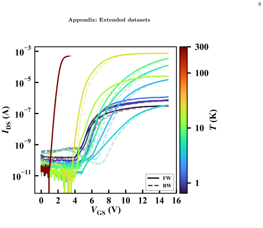
S. J. Angus, A. J. Ferguson, A. S. Dzurak, and R. G. Clark, Gate-defined quantum dots in intrinsic silicon, Nano Letters 7, 2051 (2007). 8 Appendix: Extended datasets FIG. 5. IDS-VGS transfer characteristics for Device A as a function of temperature measured with forward (solid lines) and backward (dashed lines) gate sweeps. V 0.65 K DS = 3.8 V, V 0.85 K ...
work page 2051
discussion (0)
Sign in with ORCID, Apple, or X to comment. Anyone can read and Pith papers without signing in.