A Modified Boost Converter Topology for Dynamic Characterization of Hot Carrier and Trap Generation in GaN HEMTs
Pith reviewed 2026-05-17 02:49 UTC · model grok-4.3
The pith
A modified boost converter stresses GaN HEMTs at high duty cycle to measure logarithmic R_DS(on) rise and validate phonon scattering energies.
A machine-rendered reading of the paper's core claim, the machinery that carries it, and where it could break.
Core claim
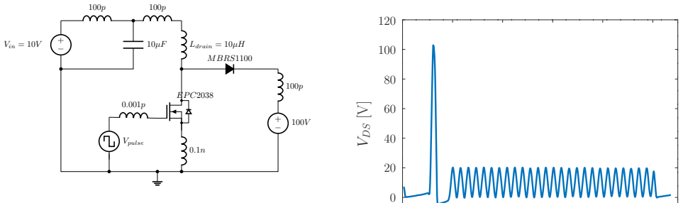
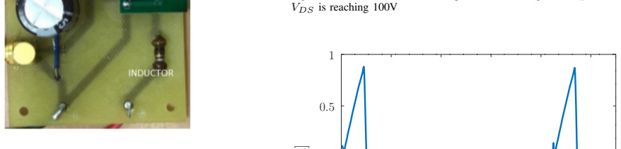
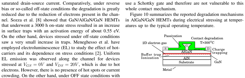
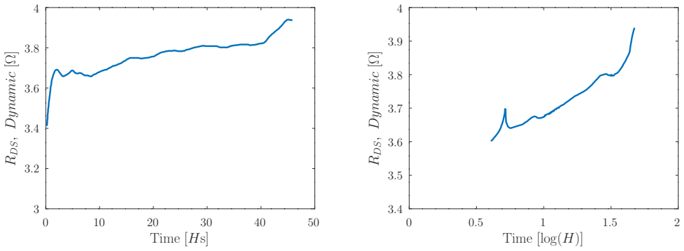
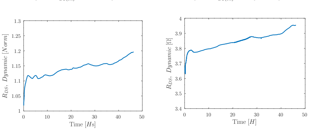
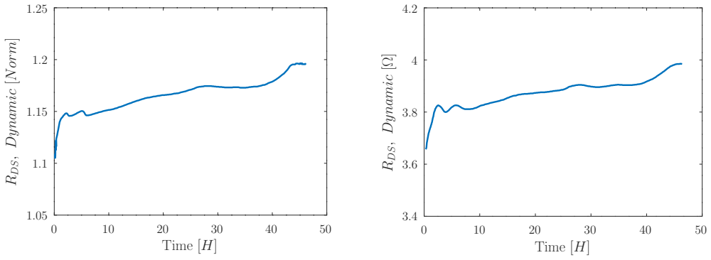
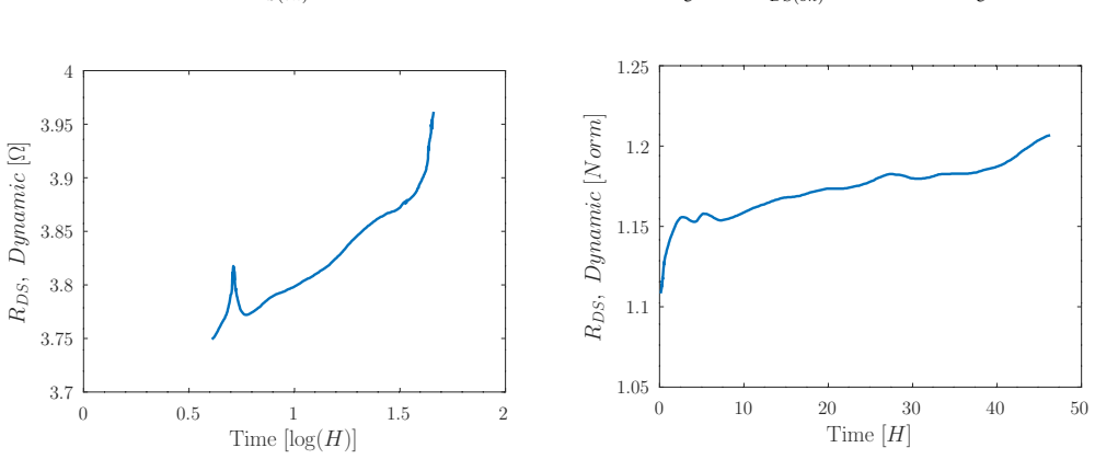
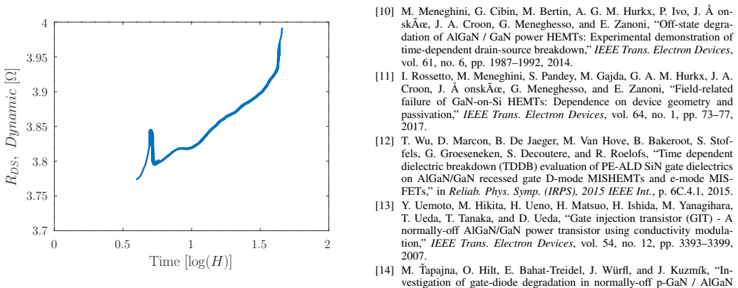
The modified boost converter applies constant 400 mA drain current at 0.7 duty cycle to an EPC 2038 GaN HEMT, producing a logarithmic rise in R_DS(on) that matches the EPC Phase 12 reliability model; stress tests at 70 V and 100 V further yield ħω_LO values that agree with existing theoretical and experimental data, thereby confirming the circuit as a tool for determining MTOL reliability factors through controlled hot carrier and trap generation.
What carries the argument
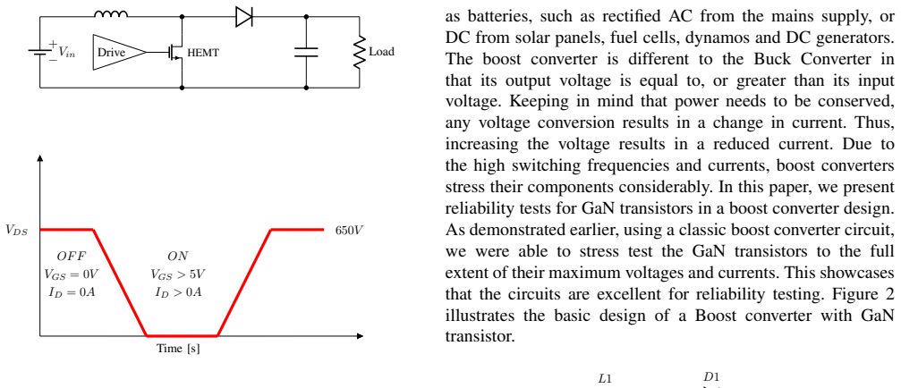
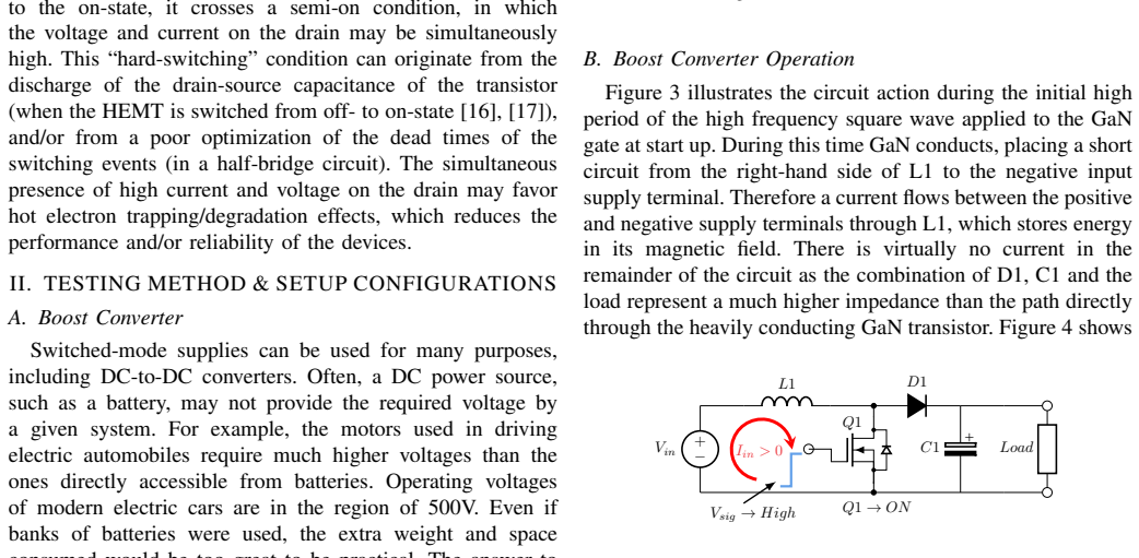
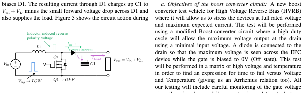
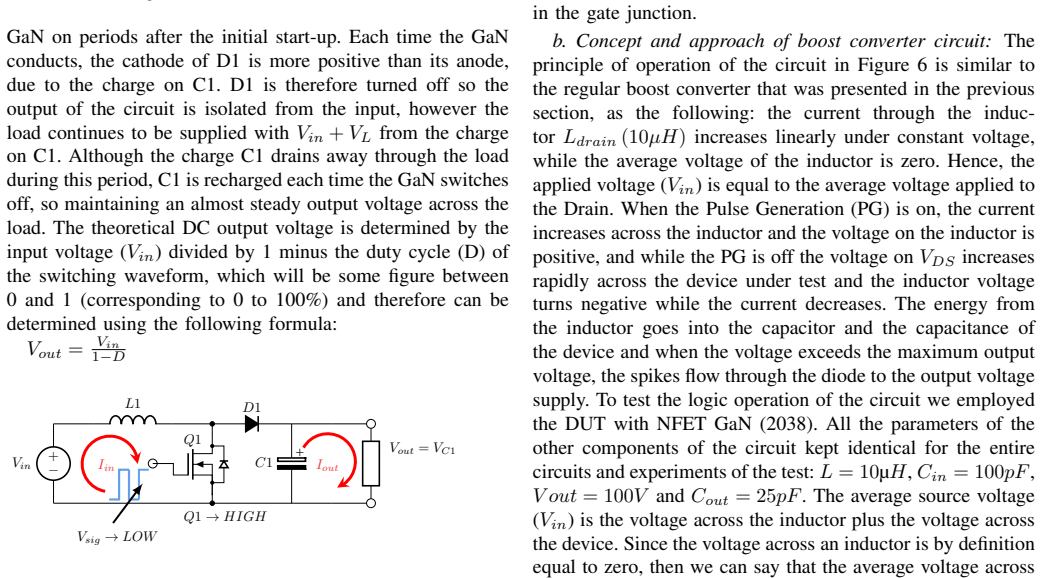
The modified boost converter topology that delivers high-duty-cycle stress at rated voltage and current while keeping input power low.
If this is right
- Device lifetime under varying voltage and current can be predicted from short accelerated tests using the same logarithmic model.
- The MTOL reliability framework gains an experimental route to extract phonon-scattering parameters directly from packaged power transistors.
- Power-electronics designers can qualify GaN HEMTs for specific operating points without full-scale high-power burn-in equipment.
Where Pith is reading between the lines
- The same converter topology could be adapted to study other wide-bandgap devices such as SiC MOSFETs by changing only the duty cycle and voltage set points.
- If the logarithmic trend holds across more device generations, manufacturers could publish standardized degradation curves derived from this low-cost test rather than proprietary high-power rigs.
- Circuit designers might incorporate the measured ħω_LO dependence into real-time temperature and bias monitors to extend safe operating area margins.
Load-bearing premise
The high-duty-cycle stress inside the converter produces the same hot-carrier and trap-generation physics that occur in normal circuit operation without adding new failure modes or measurement errors from the test setup itself.
What would settle it
An independent long-term stress test on the same GaN device under normal switching conditions shows a linear rather than logarithmic R_DS(on) increase or extracts ħω_LO values outside the accepted theoretical range.
Figures
read the original abstract
Modern microelectronic systems require long term operational stability, necessitating precise reliability models to predict device lifecycles and identify governing failure mechanisms. This is particularly critical for high power GaN High-Electron-Mobility Transistors (HEMTs), where reliability research has historically trailed behind low power digital counterparts. This study introduces a novel application of a modified boost converter circuit designed to investigate GaN failure mechanisms, specifically targeting the determination of reliability factors for the MTOL model. By utilizing a high duty cycle, the circuit stresses the device at maximum rated voltages and currents with minimal input requirements, accelerating hot carrier and trap generation without immediate detrimental failure. Experimental validation was conducted using an EPC 2038 GaN transistor under a constant drain current of 400 mA and a duty cycle of 0.7. The results confirmed that the increase in Drain-Source on-resistance ($R_{DS(on)}$) follows a logarithmic trend over time, consistent with the EPC Phase 12 reliability model. While initial tests at 40V did not successfully validate the longitudinal optical phonon scattering energy ($\hbar\omega_{LO}$), but were reasonably acceptable, subsequent stress tests at 70V and 100V yielded $\hbar\omega_{LO}$ values that were successfully validated against existing theoretical and experimental data. This methodology provides a robust framework for predicting performance and lifetime across varying operational parameters in modern power electronics.
Editorial analysis
A structured set of objections, weighed in public.
Referee Report
Summary. The paper proposes a modified boost converter topology to dynamically stress GaN HEMTs and characterize hot-carrier and trap generation for reliability modeling (MTOL). Using an EPC 2038 device stressed at constant 400 mA drain current and 0.7 duty cycle, the authors report a logarithmic rise in R_DS(on) consistent with the EPC Phase 12 model; ħω_LO values extracted at 70 V and 100 V are stated to match existing theoretical and experimental data, while the 40 V test yielded only partial success.
Significance. If the measured degradation can be shown to arise solely from intrinsic hot-carrier and trap mechanisms without confounding contributions from the switching circuit, the approach would offer a practical, low-input-power method for accelerated reliability testing of power GaN devices. The reported consistency with an established model is a positive indicator, but the absence of raw data, error bars, extraction details, and controls for circuit artifacts currently limits the strength of this contribution.
major comments (2)
- [Abstract] Abstract (experimental validation paragraph): the claim that ħω_LO values at 70 V and 100 V 'were successfully validated' is not supported by any description of the extraction procedure, fitting method, uncertainty quantification, or comparison plots; without these the validation cannot be assessed as independent of the reference data.
- [Abstract] Abstract and circuit description: the high-duty-cycle (0.7) boost-converter stress necessarily includes hard-switching transients, inductor ripple, and possible drain voltage overshoot, yet no section quantifies or subtracts these circuit-specific contributions (e.g., via DC-bias control experiments or in-situ waveform monitoring). This leaves open the possibility that part of the observed R_DS(on) rise is an artifact rather than intrinsic hot-carrier physics, directly undermining the central claim that the topology enables clean dynamic characterization.
minor comments (2)
- [Abstract] Abstract: the phrasing 'did not successfully validate ... but were reasonably acceptable' is ambiguous and should be replaced with a clear statement of the quantitative criteria used for validation.
- [Abstract] Abstract: no error bars, number of devices tested, or statistical analysis of the R_DS(on) time series are mentioned; these should be added to allow readers to judge the reliability of the logarithmic trend.
Simulated Author's Rebuttal
We thank the referee for the constructive comments on our manuscript. We address each major point below and outline the revisions we will make to strengthen the presentation of the experimental validation and circuit considerations.
read point-by-point responses
-
Referee: [Abstract] Abstract (experimental validation paragraph): the claim that ħω_LO values at 70 V and 100 V 'were successfully validated' is not supported by any description of the extraction procedure, fitting method, uncertainty quantification, or comparison plots; without these the validation cannot be assessed as independent of the reference data.
Authors: We agree that the abstract lacks sufficient detail on the ħω_LO extraction. The values were obtained by fitting the measured logarithmic R_DS(on) rise to the MTOL model form used in the EPC Phase 12 framework, with the slope parameter directly yielding the phonon energy; these were then compared numerically to the accepted 0.09 eV theoretical value and prior experimental reports. Multiple devices were measured to estimate variability. We will revise the abstract to include a concise description of the fitting procedure and uncertainty, and we will add a dedicated figure showing the data, fits, and literature comparison in the revised manuscript. revision: yes
-
Referee: [Abstract] Abstract and circuit description: the high-duty-cycle (0.7) boost-converter stress necessarily includes hard-switching transients, inductor ripple, and possible drain voltage overshoot, yet no section quantifies or subtracts these circuit-specific contributions (e.g., via DC-bias control experiments or in-situ waveform monitoring). This leaves open the possibility that part of the observed R_DS(on) rise is an artifact rather than intrinsic hot-carrier physics, directly undermining the central claim that the topology enables clean dynamic characterization.
Authors: The concern about possible circuit artifacts is valid and merits explicit discussion. The observed degradation exhibits a clean logarithmic time dependence that matches the established hot-carrier model across the 70 V and 100 V conditions, which is inconsistent with typical transient-induced mechanisms that produce different kinetics. Inductor selection and layout were chosen to limit ripple, and voltage overshoot was monitored during setup. We will expand the circuit description section to include measured waveform captures, estimated ripple and overshoot values from simulation and experiment, and a brief analysis arguing that these do not dominate the long-term logarithmic trend. Full DC-bias-only control experiments lie outside the present scope but will be noted as recommended future work. revision: partial
Circularity Check
No circularity: experimental measurements compared to external models and data
full rationale
The manuscript describes an experimental apparatus (modified boost converter) that applies high-duty-cycle stress to an EPC 2038 GaN HEMT and records the time evolution of R_DS(on). The observed logarithmic rise is reported as consistent with the pre-existing EPC Phase 12 model, and ħω_LO values extracted at 70 V and 100 V are stated to match independent theoretical and experimental literature. No equations, fitted parameters, or self-citations are shown that would make the reported trends or extracted energies equivalent to the input data by construction. The central claims rest on direct measurement and external comparison rather than on any self-referential derivation chain.
Axiom & Free-Parameter Ledger
axioms (1)
- domain assumption The MTOL model provides the correct framework for extracting reliability factors from hot-carrier and trap data in GaN HEMTs
Lean theorems connected to this paper
-
IndisputableMonolith/Cost/FunctionalEquation.leanwashburn_uniqueness_aczel unclear?
unclearRelation between the paper passage and the cited Recognition theorem.
The results confirmed that the increase in Drain-Source on-resistance (R_DS(on)) follows a logarithmic trend over time, consistent with the EPC Phase 12 reliability model... ħω_LO values that were successfully validated against existing theoretical and experimental data.
What do these tags mean?
- matches
- The paper's claim is directly supported by a theorem in the formal canon.
- supports
- The theorem supports part of the paper's argument, but the paper may add assumptions or extra steps.
- extends
- The paper goes beyond the formal theorem; the theorem is a base layer rather than the whole result.
- uses
- The paper appears to rely on the theorem as machinery.
- contradicts
- The paper's claim conflicts with a theorem or certificate in the canon.
- unclear
- Pith found a possible connection, but the passage is too broad, indirect, or ambiguous to say the theorem truly supports the claim.
Reference graph
Works this paper leans on
-
[1]
M. Meneghini, G. Meneghesso, and E. Zanoni,Power GaN devices: Materials, applications and reliability. Springer, 2017
work page 2017
-
[2]
Novel AlInN / GaN integrated circuits operating up to 500 ◦c,
R. Gaska, M. Gaevski, J. Deng, and R. Jain, “Novel AlInN / GaN integrated circuits operating up to 500 ◦c,” inProc. Solid State Device Res. Conf. (ESSDERC), 44th Eur., pp. 142–145, 2014
work page 2014
-
[3]
G. Orr, M. Azoulay, G. Golan, and A. Burger, “Gallium Ni- tride High-Electron-Mobility Transistor-Based High-Energy Particle- Detection Preamplifier,”Metrology, vol. 5, no. 2, p. 21, 2025
work page 2025
-
[4]
1900v,1.6mΩcm 2 AlN/GaN- on-Si power devices realized by local substrate removal,
N. Herbecq, I. Roch-Jeune, N. Rolland, D. Visalli, J. Derluyn, S. Deg- roote, M. Germain, and F. Medjdoub, “1900v,1.6mΩcm 2 AlN/GaN- on-Si power devices realized by local substrate removal,”Appl. Phys. Express, vol. 7, p. 034103, 2014
work page 2014
-
[5]
J.-T. Chen, I. Persson, D. Nilsson, C.-W. Hsu, J. Palisaitis, U. Fors- berg, P. O. Persson, and E. Janzén, “Room-temperature mobility above 2200cm 2/v· s of two-dimensional electron gas in a sharp-interface AlGaN/GaN heterostructure,”Applied Physics Letters, vol. 106, no. 25, 2015
work page 2015
-
[6]
Gs66516t top-side cooled 650 v e-mode GaN transistor preliminary datasheet
“Gs66516t top-side cooled 650 v e-mode GaN transistor preliminary datasheet.” http://www.gansystems.com/datasheets/GS66516T\%20DS\ %20Rev\%20161007.pdf
-
[7]
G. Orr and M. Roth, “Safe and consistent method of spot-welding plat- inum thermocouple wires and foils for high temperature measurements,” Review of scientific instruments, vol. 83, no. 8, 2012
work page 2012
-
[8]
Impact of buffer leakage on intrinsic reliability of 650v AlGaN / GaN HEMTs,
P. Moens, A. Banerjee, M. J. Uren, M. Meneghini, S. Karboyan, I. Chatterjee, P. Vanmeerbeek, M. CÃ Csar, C. Liu, A. Salih, E. Zanoni, G. Meneghesso, M. Kuball, and M. Tack, “Impact of buffer leakage on intrinsic reliability of 650v AlGaN / GaN HEMTs,” inIEEE Electron Device Meet. IEDM 2015 Techical Dig., pp. 903–906, 2015
work page 2015
-
[9]
Kinetics of buffer-relatedr on-increase in GaN-on-Silicon MISHEMTs,
D. Bisi, M. Meneghini, F. A. Marino, D. Marcon, S. Stoffels, M. Van Hove, S. Decoutere, G. Meneghesso, and E. Zanoni, “Kinetics of buffer-relatedr on-increase in GaN-on-Silicon MISHEMTs,”IEEE Electron Device Lett., vol. 35, no. 10, pp. 1004–1006, 2014
work page 2014
-
[10]
M. Meneghini, G. Cibin, M. Bertin, A. G. M. Hurkx, P. Ivo, J. Å on- skÃœ, J. A. Croon, G. Meneghesso, and E. Zanoni, “Off-state degra- dation of AlGaN / GaN power HEMTs: Experimental demonstration of time-dependent drain-source breakdown,”IEEE Trans. Electron Devices, vol. 61, no. 6, pp. 1987–1992, 2014
work page 1987
-
[11]
Field-related failure of GaN-on-Si HEMTs: Dependence on device geometry and passivation,
I. Rossetto, M. Meneghini, S. Pandey, M. Gajda, G. A. M. Hurkx, J. A. Croon, J. Å onskÃœ, G. Meneghesso, and E. Zanoni, “Field-related failure of GaN-on-Si HEMTs: Dependence on device geometry and passivation,”IEEE Trans. Electron Devices, vol. 64, no. 1, pp. 73–77, 2017
work page 2017
-
[12]
T. Wu, D. Marcon, B. De Jaeger, M. Van Hove, B. Bakeroot, S. Stof- fels, G. Groeseneken, S. Decoutere, and R. Roelofs, “Time dependent dielectric breakdown (TDDB) evaluation of PE-ALD SiN gate dielectrics on AlGaN/GaN recessed gate D-mode MISHEMTs and e-mode MIS- FETs,” inReliab. Phys. Symp. (IRPS), 2015 IEEE Int., p. 6C.4.1, 2015
work page 2015
-
[13]
Y . Uemoto, M. Hikita, H. Ueno, H. Matsuo, H. Ishida, M. Yanagihara, T. Ueda, T. Tanaka, and D. Ueda, “Gate injection transistor (GIT) - A normally-off AlGaN/GaN power transistor using conductivity modula- tion,”IEEE Trans. Electron Devices, vol. 54, no. 12, pp. 3393–3399, 2007
work page 2007
-
[14]
M. ˇTapajna, O. Hilt, E. Bahat-Treidel, J. Würfl, and J. Kuzmík, “In- vestigation of gate-diode degradation in normally-off p-GaN / AlGaN / GaN high-electron-mobility transistors,”Appl. Phys. Lett., vol. 107, p. 193506, 2015
work page 2015
-
[15]
Comprehensive investigation of on-state stress on d- mode AlGaN / GaN MIS-HEMTs,
T. Wu, D. Marcon, M. B. Zahid, M. Van Hove, S. Decoutere, and G. Groeseneken, “Comprehensive investigation of on-state stress on d- mode AlGaN / GaN MIS-HEMTs,”IEEE Int. Reliab. Phys. Symp., pp. 1–7, 2013
work page 2013
-
[16]
J. Joh, N. Tipirneni, S. Pendharkar, and S. Krishnan, “Current collapse in GaN heterojunction field effect transistors for highvoltage switching applications,” inIEEE Int. Reliab. Phys. Symp. Proc., pp. 4–7, 2014
work page 2014
-
[17]
Product-level reliability of GaN devices,
S. R. Bahl, D. Ruiz, and D. S. Lee, “Product-level reliability of GaN devices,” inIEEE Int. Reliab. Phys. Symp., 2016
work page 2016
-
[18]
An improved reliability model for Si and GaN power FET,
G. Golan, M. Azoulay, T. Avraham, I. Kremenetsky, and J. B. Bernstein, “An improved reliability model for Si and GaN power FET,”Microelec- tronics Reliability, vol. 81, pp. 77–89, 2018
work page 2018
-
[19]
Role of oxygen in the off-state degradation of AlGaN/GaN high electron mobility transistors,
F. Gao, B. Lu, L. Li, and et al., “Role of oxygen in the off-state degradation of AlGaN/GaN high electron mobility transistors,”Appl. Phys. Lett., vol. 99, no. 22, p. 223506, 2011
work page 2011
-
[20]
Impact of water-assisted electrochemical reactions on the off-state degradation of AlGaN/GaN HEMTs,
F. Gao, S. Tan, J. del Alamo, and et al., “Impact of water-assisted electrochemical reactions on the off-state degradation of AlGaN/GaN HEMTs,”IEEE Trans. Electron Devices, vol. 61, no. 2, pp. 437–444, 2014
work page 2014
-
[21]
Pyroelectric proper- ties of Al(In)GaN/GaN hetero- and quantum well structures,
O. Ambacher, J. Majewski, C. Miskys, and et al., “Pyroelectric proper- ties of Al(In)GaN/GaN hetero- and quantum well structures,”J. Phys. Condens. Matter, vol. 14, no. 13, pp. 3399–3434, 2002
work page 2002
-
[22]
D. Marcon, T. Kauerauf, F. Medjdoub, and et al., “A comprehen- sive reliability investigation of the voltage-, temperature- and device geometry-dependence of the gate degradation on state-of-the-art GaN- on-Si HEMTs,” in2010 Int. Electron Devices Meeting, pp. 20.3.1– 20.3.4, 2010
work page 2010
-
[23]
Ultrathin gate oxide reliability: physical models, statistics, and characterization,
J. Suehle, “Ultrathin gate oxide reliability: physical models, statistics, and characterization,”IEEE Trans. Electron Devices, vol. 49, no. 6, pp. 958–971, 2002
work page 2002
-
[24]
Time-dependent failure of GaN-on-Si power HEMTs with p-GaN gate,
I. Rossetto, M. Meneghini, O. Hilt, and et al., “Time-dependent failure of GaN-on-Si power HEMTs with p-GaN gate,”IEEE Trans. Electron Devices, vol. 63, no. 6, pp. 2334–2339, 2016
work page 2016
-
[25]
I. Rossetto, M. Meneghini, V . Rizzato, and et al., “Study of the stability of e-mode GaN HEMTs with p-GaN gate based on combined DC and optical analysis,”Microelectron. Reliab., vol. 64, pp. 547–551, 2016
work page 2016
-
[26]
Extensive investigation of time-dependent breakdown of GaN-HEMTs submitted to off-state stress,
M. Meneghini, I. Rossetto, F. Hurkx, and et al., “Extensive investigation of time-dependent breakdown of GaN-HEMTs submitted to off-state stress,”IEEE Trans. Electron Devices, vol. 62, no. 8, pp. 2549–2554, 2015
work page 2015
-
[27]
R. Degraeve, G. Groeseneken, R. Bellens, and et al., “New insights in the relation between electron trap generation and the statistical properties of oxide breakdown,”IEEE Trans. Electron Devices, vol. 45, no. 4, pp. 904–911, 1998
work page 1998
-
[28]
Percolation models for gate oxide breakdown,
J. Stathis, “Percolation models for gate oxide breakdown,”J. Appl. Phys., vol. 86, no. 10, p. 5757, 1999
work page 1999
-
[29]
Normally-off GaN-HEMTs with p-type gate: off-state degradation, forward gate stress and ESD failure,
M. Meneghini, O. Hilt, C. Fleury, and et al., “Normally-off GaN-HEMTs with p-type gate: off-state degradation, forward gate stress and ESD failure,”Microelectron. Reliab., vol. 58, pp. 177–184, 2016
work page 2016
-
[30]
Material and electrical properties of electroless Ag-W thin film,
A. Inberg, Y . Shacham-Diamand, E. Rabinovich, G. Golan, and N. Croitoru, “Material and electrical properties of electroless Ag-W thin film,”Journal of electronic materials, vol. 30, no. 4, pp. 355–359, 2001
work page 2001
-
[31]
Demonstration of field and power dependent ESD failure in AlGaN/GaN RF HEMTs,
I. Rossetto, M. Meneghini, M. Barbato, F. Rampazzo, D. Marcon, G. Meneghesso, and E. Zanoni, “Demonstration of field and power dependent ESD failure in AlGaN/GaN RF HEMTs,”IEEE Transactions on Electron Devices, vol. 62, no. 9, pp. 2830–2836, 2015
work page 2015
-
[32]
HBM ESD robustness of GaN-on-Si Schottky diodes,
S. Chen, A. Griffoni, P. Srivastava, and et al., “HBM ESD robustness of GaN-on-Si Schottky diodes,”IEEE Trans. Device Mater. Reliab., vol. 12, no. 4, pp. 589–598, 2012
work page 2012
-
[33]
Unique ESD behavior and failure modes of AlGaN/GaN HEMTs,
B. Shankar and M. Shrivastava, “Unique ESD behavior and failure modes of AlGaN/GaN HEMTs,” in2016 IEEE Int. Reliability Physics Symp. (IRPS), pp. EL–7–1–EL–7–5, 2016
work page 2016
-
[34]
Electrical overstress in AlGaN/GaN HEMTs: Study of degradation processes,
J. Kuzmík, D. Pogány, E. Gornik, P. Javorka, and P. Kordoš, “Electrical overstress in AlGaN/GaN HEMTs: Study of degradation processes,” Solid-State Electronics, vol. 48, no. 2, pp. 271–276, 2004
work page 2004
-
[35]
Application of gold nano- particles for silicon solar cells efficiency increase,
A. Axelevitch, B. Gorenstein, and G. Golan, “Application of gold nano- particles for silicon solar cells efficiency increase,”Applied surface science, vol. 315, pp. 523–526, 2014
work page 2014
-
[36]
M. A. Khan, M. S. Shur, Q. C. Chen, and J. N. Kuznia, “Current/voltage characteristic collapse in AlGaN/GaN heterostructure insulated gate field effect transistors at high drain bias,”Electron. Lett., vol. 30, pp. 2175– 2176, Dec. 1994
work page 1994
-
[37]
The impact of surface states on the DC and RF characteristics of AlGaN/GaN HFETs,
R. Vetury, N. Q. Zhang, S. Keller, and U. K. Mishra, “The impact of surface states on the DC and RF characteristics of AlGaN/GaN HFETs,” IEEE Trans. Electron Devices, vol. 48, pp. 560–566, Mar. 2001
work page 2001
-
[38]
Si3N4/AlGaN/GaN-metal-insulator-semiconductor heterostructure field-effect transistors,
X. Hu, A. Koudymov, G. Simin, J. Yang, M. A. Khan, A. Tarakji, M. S. Shur, and R. Gaska, “Si3N4/AlGaN/GaN-metal-insulator-semiconductor heterostructure field-effect transistors,”Appl. Phys. Lett., vol. 79, pp. 2832–2834, Oct. 2001
work page 2001
-
[39]
RF characterization and transit behavior of AlGaN/GaN power HFETs,
H. Leirer, A. Vescan, R. Dietrich, A. Wieszt, and H. H. Sledzik, “RF characterization and transit behavior of AlGaN/GaN power HFETs,” IEICE Trans. Electron., vol. E84-C, no. 10, pp. 1442–1447, 2001
work page 2001
-
[40]
Novel sputtering method for Pd–Al2O3 UV transparent conductive coatings,
G. Golan and A. Axelevitch, “Novel sputtering method for Pd–Al2O3 UV transparent conductive coatings,”Microelectronics Journal, vol. 31, no. 6, pp. 469–473, 2000
work page 2000
-
[41]
Effects of SiN passivation and high-electric field on AlGaN-GaN HFET degradation,
H. Kim, R. M. Thompson, V . Tilak, T. R. Prunty, J. R. Shealy, and L. F. Eastman, “Effects of SiN passivation and high-electric field on AlGaN-GaN HFET degradation,”IEEE Electron Device Lett., vol. 24, pp. 421–423, July 2003
work page 2003
-
[42]
J. P. Ibbetson, P. T. Fini, K. D. Ness, S. P. DenBaars, J. S. Speck, and U. K. Mishra, “Polarization effects, surface states, and the source of electrons in AlGaN/GaN heterostructure field effect transistors,”Appl. Phys. Lett., vol. 77, pp. 250–252, July 2000
work page 2000
-
[43]
Critical voltage for electrical degradation of GaN high-electron mobility transistors,
J. Joh and J. del Alamo, “Critical voltage for electrical degradation of GaN high-electron mobility transistors,”IEEE Electron Device Lett., vol. 29, no. 4, pp. 287–289, 2008
work page 2008
-
[44]
Effects of RF and DC stress on AlGaN/GaN MODFETs: A low-frequency noise-based investigation,
P. Valizadeh and D. Pavlidis, “Effects of RF and DC stress on AlGaN/GaN MODFETs: A low-frequency noise-based investigation,” IEEE Transactions on Device and Materials Reliability, vol. 5, no. 3, pp. 555–563, 2005
work page 2005
discussion (0)
Sign in with ORCID, Apple, or X to comment. Anyone can read and Pith papers without signing in.