REVIEW 3 major objections 5 minor 37 references
Surface Optimization of Superconducting Aluminum Resonators for Robust Quantum Device Fabrication
T0 review · 3 major / 5 minor · reviewed 2026-08-03 · deepseek-v4-flash
Pith's one-line read Selective removal of surface oxides with HF vapor followed by phosphoric acid reduces dielectric loss in aluminum superconducting resonators by a factor of three, reaching median δ_LP ≈ 5.7×10⁻⁷ (Q ≈ 1.7 million) even after a 24-hour delay
desk verdict A useful process-engineering study with one promising etch recipe and one cautionary negative result, but the headline numbers rest on too few chips to be taken as precisely as stated. read the letter →
The pith
A machine-rendered reading of the paper's core claim, the machinery that carries it, and where it could break.
The reading
What carries the argument
The carrying mechanism is the selective two-step oxide etch: HF vapor strips silicon dioxide with high selectivity to silicon and aluminum, while undiluted phosphoric acid etches aluminum oxide with high selectivity to silicon and SiO₂. Doing both in sequence removes the oxide layers that host two-level systems (TLS)—atomic-scale defects that absorb microwave energy at low power. The performance metric that carries the comparison is the low-power loss δ_LP, extracted by fitting the photon-number dependence of the internal quality factor to a standard TLS model. The combination of a single-wafer sample set and a 24-hour delay before cooldown is what makes the result relevant to production-sty
What would settle it
Prepare at least ten resonator chips per condition from multiple wafers, randomize which chips receive the HF + phosphoric acid etch, and measure δ_LP blind. If the treated median is not separated from untreated by roughly a factor of three, or if one untreated wafer matches the treated level, the claimed ordering and factor would not hold.
Extended reading notes
Core claim
On the paper's own terms, the central discovery is that selective chemistry can remove each surface oxide independently without attacking the metal: HF vapor removes SiO₂ while leaving Al₂O₃, and undiluted phosphoric acid removes Al₂O₃ while leaving Si. Applied sequentially to otherwise untreated resonator chips and followed by a 24-hour wait in ambient air before cooldown, this two-step etch lowered the median low-power dielectric loss from the untreated level by roughly a factor of three, down to δ̃_LP = 5.7 × 10⁻⁷ (Q ≈ 1.7M), with the lower quartile at 5.2 × 10⁻⁷ (Q = 1.9M). The authors attribute the improvement to the removal of TLS-hosting oxides, consistent with the established picture
Load-bearing premise
The result rests on treating chips cut from the same 200 mm wafer as geometrically identical, so the observed factor-of-three loss gap is attributed to the chemical treatment rather than to chip-to-chip variation—and each condition uses only two chips, with some lost.
Editorial extensions
If this is right
- Aluminum resonator chips can be post-treated with a simple wet/vapor etch and still reach Q ≈ 1.7 million after sitting in air for 24 hours, a realistic industrial scheduling window.
- The factor-of-three loss reduction implies that surface oxides are a dominant, removable source of TLS loss in these devices, not an intrinsic material limit.
- Fluorinated aluminum surfaces can survive BOE without visible damage, which could enable full-chip BOE treatment in devices that combine Al junctions with Nb or Ta resonators—though at a measurable loss penalty.
- The same HF + phosphoric acid sequence may be applied to other Al-based circuits, including transmon qubit electrodes, with potential coherence gains.
- Remote oxygen plasma offers only a marginal improvement and high-power direct plasma worsens loss, so process engineers should avoid energetic ion bombardment of the resonator surfaces.
Reading between the lines
- A natural extension not tested in the paper is whether the two-step etch also reduces high-power loss or whether it only removes TLS losses, which would point toward a different set of residual loss mechanisms.
- The 24-hour delay result suggests the etched surfaces re-oxidize slowly enough to remain beneficial; extending the test to longer or humid delays would map out how long the treatment stays effective in real fabs.
- The chemical etch might be combined with the remote oxygen plasma or with argon-milling steps to push Q further, although the paper does not demonstrate such a stack.
- If the loss reduction transfers to qubit T1, the same etch could let manufacturers decouple resonator and qubit fabrication timing, easing multi-chip packaging workflows.
Editorial analysis
A structured set of objections, weighed in public.
Referee Report
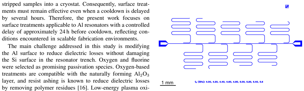
Summary. The paper investigates post-fabrication surface treatments for aluminum coplanar-waveguide resonators subject to a controlled 24-hour ambient delay before cryogenic measurement. Three approaches are compared: oxygen plasma passivation, fluorine passivation via Ar-milling plus CF4 plasma, and selective chemical etching with HF vapor and/or H3PO4. The central claim is that sequential application of HF vapor and phosphoric acid removes SiO2 and Al2O3 selectively, reducing TLS-dominated low-power loss by a factor of about three relative to untreated samples, reaching δ~LP ≈ 5.7×10^-7 and QLP ≈ 1.7–1.9 million in the single-photon regime. The paper also reports that fluorination increases loss while passivating Al against BOE, and that remote oxygen plasma modestly reduces loss. The measurements use the standard TLS loss model to extract δ_LP from S21 data on nine resonators per chip, with two chips per treatment condition.
Significance. If the central claim holds, this is a practically valuable result: a simple, wafer-compatible HF-vapor/H3PO4 etch sequence would mitigate oxide-related TLS loss in Al resonators even after a 24-hour delay, directly addressing an industrial fabrication constraint. The study is systematic in its comparison of several treatments, uses a single wafer to suppress wafer-to-wafer variability, includes XPS verification of fluorination, and is consistent with the established picture of TLS losses from surface oxides. However, the quantitative factor-of-three improvement and the robustness claim rest on a small number of chips per condition and the absence of a zero-delay control, so the experimental support is currently weaker than the abstract's definitive wording implies.
major comments (3)
- [§IV, Fig. 8] second major comment
- [§III-C, abstract] The abstract and conclusion claim that the etch sequence 'preserves low dielectric losses for a 24-hour delay before cooldown.' No zero-delay or shorter-delay control is reported, so the data only show that the treated samples are lower-loss than untreated samples after the same delay. It does not demonstrate that delay does not degrade the treated surface. A control with immediate cooldown (or at least a second delay time) is needed to support the 'robust to delay' conclusion.
- [§IV-C and abstract] There is a numerical inconsistency in the headline result. The posted abstract reports δ~LP = 5.7×10^-7 and QLP ≈ 1.7 million, while the full-text abstract and §IV-C state δLP = 5.2×10^-7 and QLP = 1.9 million, with 5.2×10^-7 described as the lower quartile. The authors should reconcile these numbers and consistently report the median, quartiles, and corresponding quality factors.
minor comments (5)
- [§II, Eq. (1)] The fit parameters n_c, β, and δ_HP are not listed or bounded. Since the extracted δ_LP is the key quantity, at least a brief statement of fit stability and uncertainty would help.
- [§IV-A] The remote-oxygen-plasma improvement is described as 'approximately 50%' but the IQRs overlap substantially. This claim should be softened or accompanied by significance testing.
- [§III-B] The XPS data in Fig. 5 show atomic fractions after the samples were milled for 1 min before XPS; the distinction between surface and bulk composition should be clarified.
- [§IV-C] The phrase 'reduced the loss by a combined factor of three' is ambiguous: is the factor relative to the untreated median, or to the medians of the individual etches? Please state the comparison explicitly.
- [General] A few minor grammatical issues and missing articles appear throughout, and the abstract's first sentence would benefit from rewording for clarity.
Circularity Check
No circularity: measured-loss comparison with standard TLS fit; no prediction reduces to fitted input.
full rationale
The paper makes no derivation-to-conclusion circular step. The central quantitative quantity, δ_LP, is an empirical fit parameter obtained from measured S21 data using the standard TLS model in Eq. (1) (Section II), and it is not used as an input to define any treatment. The key claim—that combined HF-vapor and H3PO4 etching reduces δ_LP relative to untreated samples—is a direct inter-group comparison of measured low-power losses (Section IV-C, Fig. 8), not a quantity forced by construction. The self-citations [17] and [28] supply process parameters and a fabrication-reproducibility assertion; they do not define the measured loss ordering or constitute an unverified load-bearing uniqueness claim. Even the 'geometrically identical' assumption supported by [28] concerns wafer-processing reproducibility rather than a derivation that presupposes the result. The statistical weakness (two chips per condition, lost samples, chip-to-chip variability) is an evidential/correctness concern, not circularity. The abstract/body numerical inconsistency is reportorial and does not affect the derivation chain. Therefore no significant circularity is present.
Assumptions & free parameters
free parameters (3)
- n_c (critical photon number) =
per-resonator, not reported
- β (TLS saturation exponent) =
per-resonator, not reported
- δ_HP (high-power loss floor) =
per-resonator, not reported
assumptions (4)
- domain assumption Eq.(1) describes dielectric loss with a broad TLS distribution and T→0
- domain assumption Chips from one 200 mm wafer are geometrically and electrically equivalent
- domain assumption XPS composition after 1 min Ar milling is representative of the resonator surface that determines loss
- domain assumption Removing SiO2 and Al2O3 reduces TLS loss
Cite this review
Pith. "Pith review of Surface Optimization of Superconducting Aluminum Resonators for Robust Quantum Device Fabrication." pith.science (2026). https://pith.science/paper/5WPYLWBE
@misc{pith2026260104082,
  author       = {Pith},
  title        = {Pith review of: Surface Optimization of Superconducting Aluminum Resonators for Robust Quantum Device Fabrication},
  year         = {2026},
  howpublished = {\url{https://pith.science/paper/5WPYLWBE}},
  note         = {Machine review of arXiv:2601.04082}
}
abstract
Aluminum (Al) remains the central material for superconducting qubits, and considerable effort has been devoted to optimizing its deposition and patterning for quantum devices. However, post-processing strategies focused on oxide removal of niobium (Nb) and tantalum (Ta) -based resonators using buffered oxide etch (BOE), which can not be used for Al. This challenge becomes particularly relevant for industry-scale fabrication with multi-chip bonding, where delays between sample preparation and cooldown require surface treatments that preserve low dielectric loss during extended exposure to ambient conditions. In this work, we investigate surface modification approaches for Al resonators subjected to a 24-hour delay prior to cryogenic measurement. Passivation using self-limiting oxygen and fluorine chemistries was evaluated utilizing different plasma processes. Remote oxygen plasma treatment reduced dielectric losses, in contrast to direct oxygen plasma. A fluorine-based plasma process was developed that passivated the Al surface for subsequent BOE treatment. However, the fluorine content in the surface resulted in higher loss, identifying fluorine as an unsuitable passivation material for Al resonators. Above all, selective oxide removal using HF (hydrogen fluoride) vapor and phosphoric acid yielded median dielectric losses as low as $\tilde{\delta}_\mathrm{LP} = 5.7 \times 10^{-7}$ ($Q_\mathrm{LP} \approx 1.7\,\mathrm{M}$) with $\tilde{\delta}_\mathrm{TLS} = 3.6 \times 10^{-7}$ ($Q_\mathrm{TLS} \approx 2.8\,\mathrm{M}$) in the single photon regime. Selective oxide removal provides a promising pathway for robust Al-based qubit fabrication, as it preserves low dielectric losses for a 24-hour delay before cooldown.
Figures


Figures from the paper (4 more)


Reference graph
Works this paper leans on
-
[28]
S. Lang, T. Mayer, J. Weber, C. Dhieb, I. Eisele, W. Lerch, Z. Luo, C. M. Guiz ´an, E. Music, L. Sturm-Rogon, D. Zahn, R. Pereira, and C. Kutter, “Cmos-compatible processing and room-temperature characterization at the wafer level for scalable quantum computing,” Phys. Rev. Appl., vol. 24, p. 054052, Nov 2025. [Online]. Available: https://link.aps.org/doi...
-
[1]
Methods to achieve near-millisecond energy relaxation and dephasing times for a superconducting transmon qubit,
M. Tuokkola, Y . Sunada, H. Kivij ¨arvi, J. Albanese, L. Gr ¨onberg, J.-P. Kaikkonen, V . Vesterinen, J. Govenius, and M. M ¨ott¨onen, “Methods to achieve near-millisecond energy relaxation and dephasing times for a superconducting transmon qubit,”Nat Commun, vol. 16, no. 1, p. 5421, Jul. 2025. [Online]. Available: https://www.nature.com/articles/s41467- ...
2025
-
[2]
Millisecond lifetimes and coherence times in 2D transmon qubits,
M. P. Bland, F. Bahrami, J. G. C. Martinez, P. H. Prestegaard, B. M. Smitham, A. Joshi, E. Hedrick, S. Kumar, A. Yang, A. C. Pakpour-Tabrizi, A. Jindal, R. D. Chang, G. Cheng, N. Yao, R. J. Cava, N. P. De Leon, and A. A. Houck, “Millisecond lifetimes and coherence times in 2D transmon qubits,”Nature, vol. 647, no. 8089, pp. 343–348, Nov. 2025. [Online]. A...
2025
-
[3]
Mitigation of interfacial dielectric loss in aluminum-on-silicon superconducting qubits,
J. Bizn ´arov´a, A. Osman, E. Rehnman, L. Chayanun, C. Kri ˇzan, P. Malmberg, M. Rommel, C. Warren, P. Delsing, A. Yurgens, J. Bylander, and A. Fadavi Roudsari, “Mitigation of interfacial dielectric loss in aluminum-on-silicon superconducting qubits,”npj Quantum Information, vol. 10, no. 1, p. 78, Aug. 2024. [Online]. Available: https://doi.org/10.1038/s4...
-
[4]
S. Fritz, L. Radtke, R. Schneider, M. Weides, and D. Gerthsen, “Optimization of al/alox/al-layer systems for josephson junctions from a microstructure point of view,”Journal of Applied Physics, vol. 125, no. 16, p. 165301, 04 2019. [Online]. Available: https://doi.org/10.1063/1.5089871
-
[5]
Investigation of Microwave Loss Induced by Oxide Regrowth in High-Q Niobium Resonators,
J. Verjauw, A. Poto ˇcnik, M. Mongillo, R. Acharya, F. Mohiyaddin, G. Simion, A. Pacco, T. Ivanov, D. Wan, A. Vanleenhove, L. Souriau, J. Jussot, A. Thiam, J. Swerts, X. Piao, S. Couet, M. Heyns, B. Govoreanu, and I. Radu, “Investigation of Microwave Loss Induced by Oxide Regrowth in High-Q Niobium Resonators,”Phys. Rev. Appl., vol. 16, no. 1, p. 014018, ...
-
[6]
Localization and Mitigation of Loss in Niobium Superconducting Circuits,
M. V . P. Alto ´e, A. Banerjee, C. Berk, A. Hajr, A. Schwartzberg, C. Song, M. Alghadeer, S. Aloni, M. J. Elowson, J. M. Kreikebaum, E. K. Wong, S. M. Griffin, S. Rao, A. Weber-Bargioni, A. M. Minor, D. I. Santiago, S. Cabrini, I. Siddiqi, and D. F. Ogletree, “Localization and Mitigation of Loss in Niobium Superconducting Circuits,”PRX Quantum, vol. 3, no...
-
[7]
Nitrogen plasma passivated niobium resonators for superconducting quantum circuits,
K. Zheng, D. Kowsari, N. J. Thobaben, X. Du, X. Song, S. Ran, E. A. Henriksen, D. S. Wisbey, and K. W. Murch, “Nitrogen plasma passivated niobium resonators for superconducting quantum circuits,”Applied Physics Letters, vol. 120, no. 10, p. 102601, Mar. 2022. [Online]. Avail- able: https://pubs.aip.org/apl/article/120/10/102601/2833153/Nitrogen- plasma-pa...
2022
Show all 37 references
-
[8]
Oxygen vacancies in niobium pentoxide as a source of two- level system losses in superconducting niobium,
D. Bafia, A. Murthy, A. Grassellino, and A. Romanenko, “Oxygen vacancies in niobium pentoxide as a source of two- level system losses in superconducting niobium,”Phys. Rev. Appl., vol. 22, p. 024035, Aug 2024. [Online]. Available: https://link.aps.org/doi/10.1103/PhysRevApplie...
2024 doi
-
[9]
Low-loss superconducting resonators fabricated from tantalum films grown at room temperature,
G. Marcaud, D. Perello, C. Chen, E. Umbarkar, C. Weiland, J. Gao, S. Diez, V . Ly, N. Mahuli, N. D’Souza, Y . He, S. Aghaeimeibodi, R. Resnick, C. Jaye, A. K. Rumaiz, D. A. Fischer, M. Hunt, O. Painter, and I. Jarrige, “Low-loss superconducting resonators fabricated from tanta...
2025
-
[10]
Disentangling losses in tantalum superconducting circuits,
K. D. Crowley, R. A. McLellan, A. Dutta, N. Shumiya, A. P. M. Place, X. H. Le, Y . Gang, T. Madhavan, M. P. Bland, R. Chang, N. Khedkar, Y . C. Feng, E. A. Umbarkar, X. Gui, L. V . H. Rodgers, Y . Jia, M. M. Feldman, S. A. Lyon, M. Liu, R. J. Cava, A. A. Houck, and N. P. de Le...
2023 doi
-
[11]
Improving the lifetime of aluminum-based superconducting qubits through atomic layer etching and deposition,
N. Mahuli, J. Minguzzi, J. Gao, R. Resnick, S. Diez, R. Cosmic, G. Marcaud, M. Hunt, L. Swenson, J. Rose, O. Painter, and I. Jarrige, “Improving the lifetime of aluminum-based superconducting qubits through atomic layer etching and deposition,”ACS Nano, vol. 19, no. 48, pp. 41...
2025 doi
-
[12]
High-Q trenched aluminum coplanar resonators with an ultrasonic edge microcutting for superconducting quantum devices,
E. V . Zikiy, A. I. Ivanov, N. S. Smirnov, D. O. Moskalev, V . I. Polozov, A. R. Matanin, E. I. Malevannaya, V . V . Echeistov, T. G. Konstantinova, and I. A. Rodionov, “High-Q trenched aluminum coplanar resonators with an ultrasonic edge microcutting for superconducting quant...
2023
-
[13]
Eliminating Surface Oxides of Superconducting Circuits with Noble Metal Encapsulation,
R. D. Chang, N. Shumiya, R. A. McLellan, Y . Zhang, M. P. Bland, F. Bahrami, J. Mun, C. Zhou, K. Kisslinger, G. Cheng, B. M. Smitham, A. C. Pakpour-Tabrizi, N. Yao, Y . Zhu, M. Liu, R. J. Cava, S. Gopalakrishnan, A. A. Houck, and N. P. de Leon, “Eliminating Surface Oxides of S...
2025 doi
-
[14]
Experimental evidence for a surface distribution of two-level systems in superconducting lithographed microwave resonators,
J. Gao, M. Daal, A. Vayonakis, S. Kumar, J. Zmuidzinas, B. Sadoulet, B. A. Mazin, P. K. Day, and H. G. Leduc, “Experimental evidence for a surface distribution of two-level systems in superconducting lithographed microwave resonators,”Applied Physics Letters, vol. 92, no. 15, ...
2008
-
[15]
Towards understanding two- level-systems in amorphous solids: insights from quantum circuits,
C. M ¨uller, J. H. Cole, and J. Lisenfeld, “Towards understanding two- level-systems in amorphous solids: insights from quantum circuits,” Rep. Prog. Phys., vol. 82, no. 12, p. 124501, Dec. 2019. [Online]. Available: https://iopscience.iop.org/article/10.1088/1361-6633/ab3a7e
2019 doi
-
[16]
Characterization and reduction of microfabrication-induced decoherence in superconducting quantum circuits,
C. M. Quintana, A. Megrant, Z. Chen, A. Dunsworth, B. Chiaro, R. Barends, B. Campbell, Y . Chen, I.-C. Hoi, E. Jeffrey, J. Kelly, J. Y . Mutus, P. J. J. O’Malley, C. Neill, P. Roushan, D. Sank, A. Vainsencher, J. Wenner, T. C. White, A. N. Cleland, and J. M. Martinis, “Charact...
2014
-
[17]
Aluminum Josephson junction formation on 200mm wafers using different oxidation techniques,
S. Lang, A. Schewski, I. Eisele, C. Kutter, and W. Lerch, “Aluminum Josephson junction formation on 200mm wafers using different oxidation techniques,”ECS Transactions, vol. 111, no. 1, pp. 41–52, May 2023. [Online]. Available: https://iopscience.iop.org/article/10.1149/11101.0041ecst
2023 arXiv
-
[18]
J. R. Rumble, Ed.,CRC Handbook of Chemistry and Physics, 103rd ed. Boca Raton, FL: CRC Press, Taylor & Francis Group, 2022
2022
-
[19]
Atomic layer etching of Al2O3 with NF3 plasma fluorination and trimethylaluminum ligand exchange,
J. Kim, D. Shim, Y . Kim, and H. Chae, “Atomic layer etching of Al2O3 with NF3 plasma fluorination and trimethylaluminum ligand exchange,”Journal of Vacuum Science & Technology A, vol. 40, no. 3, p. 032603, May 2022. [Online]. Available: https://pubs.aip.org/jva/article/40/3/0...
2022
-
[20]
Chemical sputtering of Al2O3 by fluorine-containing plasmas excited by electron cyclotron resonance,
Y . H. Lee, Z. H. Zhou, D. A. Danner, P. M. Fryer, and J. M. Harper, “Chemical sputtering of Al2O3 by fluorine-containing plasmas excited by electron cyclotron resonance,”Journal of Applied Physics, vol. 68, no. 10, pp. 5329–5336, Nov. 1990. [Online]. Available: https://pubs.a...
1990
-
[21]
CF4 plasma-based atomic layer etching of Al2O3 and surface smoothing effect,
C.-W. Chen, W.-H. Cho, C.-Y . Chang, C.-Y . Su, N.-N. Chu, C.-C. Kei, and B.-R. Li, “CF4 plasma-based atomic layer etching of Al2O3 and surface smoothing effect,”Journal of Vacuum Science & Technology A, vol. 41, no. 1, p. 012602, Jan. 2023. [Online]. Avail- able: https://pubs...
2023
-
[22]
Decoherence in Josephson Qubits from Dielectric Loss,
J. M. Martinis, K. B. Cooper, R. McDermott, M. Steffen, M. Ansmann, K. D. Osborn, K. Cicak, S. Oh, D. P. Pappas, R. W. Simmonds, and C. C. Yu, “Decoherence in Josephson Qubits from Dielectric Loss,” Phys. Rev. Lett., vol. 95, no. 21, p. 210503, Nov. 2005. [Online]. Available: ...
2005 doi
-
[23]
Materials loss measurements using superconducting microwave resonators,
C. R. H. McRae, H. Wang, J. Gao, M. R. Vissers, T. Brecht, A. Dunsworth, D. P. Pappas, and J. Mutus, “Materials loss measurements using superconducting microwave resonators,”Review of Scientific Instruments, vol. 91, no. 9, p. 091101, 09 2020. [Online]. Available: https://doi....
2020 doi
-
[24]
R. N. Simons,Coplanar Waveguide Circuits, Components, and Systems, 1st ed. Wiley, Mar. 2001. [Online]. Available: https://onlinelibrary.wiley.com/doi/book/10.1002/0471224758
2001 doi
-
[25]
Coplanar waveguide resonators for circuit quantum electrodynamics,
M. G ¨oppl, A. Fragner, M. Baur, R. Bianchetti, S. Filipp, J. M. Fink, P. J. Leek, G. Puebla, L. Steffen, and A. Wallraff, “Coplanar waveguide resonators for circuit quantum electrodynamics,”Journal of Applied Physics, vol. 104, no. 11, p. 113904, Dec. 2008. [Online]. Avail- a...
2008
-
[26]
Efficient and robust analysis of complex scattering data under noise in microwave resonators,
S. Probst, F. B. Song, P. A. Bushev, A. V . Ustinov, and M. Weides, “Efficient and robust analysis of complex scattering data under noise in microwave resonators,”Review of Scientific Instruments, vol. 86, no. 2, p. 024706, Feb. 2015
2015
-
[27]
Reducing intrinsic loss in superconducting resonators by surface treatment and deep etching of silicon substrates,
A. Bruno, G. de Lange, S. Asaad, K. L. van der Enden, N. K. Langford, and L. DiCarlo, “Reducing intrinsic loss in superconducting resonators by surface treatment and deep etching of silicon substrates,”Applied Physics Letters, vol. 106, no. 18, p. 182601, May 2015
2015
-
[29]
Low-temperature processing of semiconductor surfaces by use of a high-density microwave plasma,
W. Lerch, A. Gschwandtner, S. Schneider, T. Theiler, Z. Nenyei, B. Peuse, and Y . Hu, “Low-temperature processing of semiconductor surfaces by use of a high-density microwave plasma,”Semicond. Sci. Technol., vol. 24, no. 5, p. 052001, May 2009. [Online]. Available: https://iop...
2009 doi
-
[30]
K ¨ohler, ¨Atzverfahren f¨ur die Mikrotechnik, 1st ed
M. K ¨ohler, ¨Atzverfahren f¨ur die Mikrotechnik, 1st ed. Weinheim: Wiley- VCH, 1998, englische Ausgabe alsEtching in Microsystem Technology, 1999
1998
-
[31]
Koch and T
C. Koch and T. J. Rinke,Fotolithografie: Grundlagen der Mikrostruk- turierung. Ulm, Germany: MicroChemicals GmbH, 2017
2017
-
[32]
Microwave dielectric loss at single photon energies and millikelvin temperatures,
A. D. O’Connell, M. Ansmann, R. C. Bialczak, M. Hofheinz, N. Katz, E. Lucero, C. McKenney, M. Neeley, H. Wang, E. M. Weig, A. N. Cleland, and J. M. Martinis, “Microwave dielectric loss at single photon energies and millikelvin temperatures,”Applied Physics Letters, vol. 92, no...
2008
-
[33]
Low-loss superconducting resonant circuits using vacuum-gap-based microwave components,
K. Cicak, D. Li, J. A. Strong, M. S. Allman, F. Altomare, A. J. Sirois, J. D. Whittaker, J. D. Teufel, and R. W. Simmonds, “Low-loss superconducting resonant circuits using vacuum-gap-based microwave components,”Applied Physics Letters, vol. 96, no. 9, p. 093502, Mar. 2010. [O...
2010
-
[34]
A Comparison of CF4, CHF3 and C4F8 + Ar/O2 Inductively Coupled Plasmas for Dry Etching Applications,
N. Lim, A. Efremov, and K.-H. Kwon, “A Comparison of CF4, CHF3 and C4F8 + Ar/O2 Inductively Coupled Plasmas for Dry Etching Applications,”Plasma Chem Plasma Process, vol. 41, no. 6, pp. 1671–1689, Nov. 2021. [Online]. Available: https://link.springer.com/10.1007/s11090-021-10198-z
2021 doi
-
[35]
Expression of the Si Etch Rate in a CF 4 Plasma with Four Internal Process Variables,
B.-O. Cho, S.-W. Hwang, I.-W. Kim, and S. H. Moon, “Expression of the Si Etch Rate in a CF 4 Plasma with Four Internal Process Variables,” J. Electrochem. Soc., vol. 146, no. 1, pp. 350–358, Jan. 1999. [Online]. Available: https://iopscience.iop.org/article/10.1149/1.1391612
1999 doi
-
[36]
Argon-Milling-Induced Decoherence Mechanisms in Superconducting Quantum Circuits,
J. Van Damme, T. Ivanov, P. Favia, T. Conard, J. Verjauw, R. Acharya, D. Perez Lozano, B. Raes, J. Van De V ondel, A. Vadiraj, M. Mongillo, D. Wan, J. De Boeck, A. Poto ˇcnik, and K. De Greve, “Argon-Milling-Induced Decoherence Mechanisms in Superconducting Quantum Circuits,”P...
2023 doi
-
[37]
Optimizing cmos-compatible titanium nitride resonators: Deposition conditions and structuring processes,
S. J. K. Lang, A. Schewski, I. Eisele, J. Weber, C. M. Guiz ´an, Z. Lou, M. Singer, B. Schoof, T. Mayer, D. Zahn, R. N. Pereira, M. Tornow, and C. Kutter, “Optimizing cmos-compatible titanium nitride resonators: Deposition conditions and structuring processes,” Munich, Germany...
2026
Reviewed August 3, 2026 · model on record in the stance chip above.
Discussion (0). Continue with ORCID to comment.