REVIEW 3 major objections 4 minor 43 references
All stacking faults in both phases of GaN act as type II interfaces that locally reduce the band gap.
Reviewed by Pith at T0; open to challenge. T0 means a machine referee read the full paper against a public rubric. the ladder, T0–T4 →
T0 review · deepseek-v4-flash
2026-08-03 10:05 UTC pith:ON2ZH44L
load-bearing objection First DFT study of zb-GaN stacking faults with a plausible but under-supported claim that all SFs are type II. the 3 major comments →
DFT modelling of stacking faults in hexagonal and cubic GaN
The pith
A machine-rendered reading of the paper's core claim, the machinery that carries it, and where it could break.
Core claim
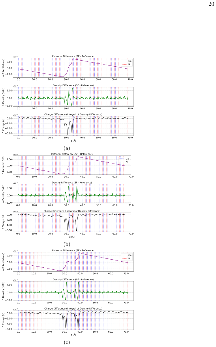
The authors show that all seven stacking faults considered form type II band alignments: at each fault, both the valence band maximum and conduction band minimum rise to higher energies than in the bulk, and they localize on opposite sides of the fault plane. The local band gap is reduced by roughly 0.01 to 0.1 eV, with zincblende faults showing the larger reductions. This behavior is traced to a charge redistribution across the fault that creates an electrostatic potential step, which in wurtzite is opposite in sign to that in zincblende. The finding overturns the common 'inclusion' model of stacking faults in zincblende GaN as wurtzite insertions, since a wurtzite inclusion would locally r
What carries the argument
The central tool is the comparison of band edges between faulted supercells and perfect bulk using a common energy reference: the upper group of semi-core Ga d-bands, which has less than 0.1 eV dispersion, is aligned at the gamma point to set the zero. With this reference, the paper computes conduction and valence band offsets for each fault and classifies the alignment as type I or type II. The mechanism behind the offsets is established using band-resolved charge densities and the planar-averaged electrostatic potential difference between faulted and perfect cells, which shows how charge transfer across the fault creates the potential step that separates the band extrema spatially.
Load-bearing premise
The band-offset and gap-reduction conclusions assume that the upper group of semi-core Ga d-bands is an exact, transferable energy reference between a cell containing a stacking fault and a perfect bulk cell; if that reference shifts at the fault by just a few meV, the smallest reported offset (0.005 eV for the I1 fault) and the type II assignment for that fault would not hold.
What would settle it
Repeat the band-offset calculation for the I1 fault using a hybrid functional or GW, or align the supercell bands using core-level energies or the macroscopic average electrostatic potential far from the fault, and check whether the CBM offset stays at +5 meV; alternatively, map the local band gap across an isolated I1 fault with sub-10 meV energy resolution using low-temperature scanning tunneling spectroscopy.
If this is right
- I1 is confirmed as the most stable stacking fault in wurtzite GaN, with a formation energy near 17 mJ/m², matching the experimental dominance of I1 faults in epilayers.
- All three zincblende stacking faults have negative formation energies close to –33 mJ/m², so faults should form readily and with comparable abundance in cubic GaN.
- Because each fault locally narrows the gap and separates electrons from holes, stacking faults are expected to act as low-energy recombination centers, consistent with cathodoluminescence and photoluminescence lines seen below the bulk band edge.
- The type II classification rules out the common 'phase-inclusion' model of faults in optoelectronic device simulations; models that treat a fault as a quantum well of the other polymorph would misplace the band edges.
Where Pith is reading between the lines
- If this type II picture is confirmed by higher-level electronic-structure methods, stacking faults could be viewed as pre-existing charge-separation elements in GaN, potentially useful in photovoltaic or photocatalytic designs rather than only as harmful defects.
- The I1 fault's conduction-band offset of about +5 meV is smaller than the quoted ≈0.1 eV dispersion of the d-band reference, so the type II classification of the most common wurtzite fault is the least numerically robust result in the paper.
- The same charge-redistribution-and-potential-step mechanism should apply to other polymorphic III-V and II-VI semiconductors (e.g., AlN, InN, ZnS), suggesting a general rule that stacking faults in tetrahedrally bonded crystals introduce type II band offsets.
- Since the three zincblende fault types are nearly degenerate in energy, any observed preference among them in growth comes from kinetics or local strain, not from thermodynamic stability, which could guide interpretation of transmission-electron-microscopy surveys.
Editorial analysis
A structured set of objections, weighed in public.
Referee Report
Summary. The paper reports PBE-DFT calculations of stacking faults in wurtzite and zincblende GaN using the Conquest code with a PAO DZP basis. It considers all intrinsic, extrinsic, and twin fault geometries, computes formation energies, interplanar spacings, band-resolved charge densities, electrostatic potentials, projected DOS, and band offsets. The main claim is that all stacking faults in both phases form type II band alignments with a locally reduced band gap, contradicting the simple model of SFs as inclusions of the other phase. The formation-energy ordering for wurtzite (I1 < I2 < I3 < E) agrees with experiment, while all zincblende faults have similar, slightly negative formation energies. The paper includes convergence tests for the formation energies and makes the data openly available.
Significance. If the electronic-structure conclusions are robust, the paper would provide a systematic reference for how stacking faults modify the band edges of GaN, with implications for device modeling and for interpreting optical spectra. The study covers all fault types in both polytypes, which is a useful contribution. The formation-energy calculations are carefully converged with respect to cell size and match the known experimental preference for the I1 fault. However, the central band-offset and gap-reduction results rest on energy differences of 5–40 meV, and the paper currently provides no uncertainty estimates or validation of the common-reference scheme used for those offsets. The open data and detailed supporting information are strengths, but the quantitative electronic-structure claims are not yet secured to the precision required.
major comments (3)
- [Sec. II and Table VI (Appendix F)] The common energy zero is the Γ-point value of the upper semi-core Ga d-band group, justified by its <0.1 eV dispersion. However, the decisive I1 wz offsets in Table VI are ΔE_C = +0.005 eV and ΔE_g = −0.015 eV, an order of magnitude smaller than the reference dispersion. No test is reported showing that the d-band position relative to the VBM (or to the macroscopic average potential) is unchanged by the presence of the fault. Furthermore, the same table quotes Ref. [16] as giving ΔE_C = −0.045 eV for the same I1 fault, opposite in sign. Since the sign of ΔE_C is what distinguishes type II from type I, the central electronic-structure conclusion is not secured against a few-meV shift of the reference. The authors should validate the reference transferability (e.g., by computing offsets with macroscopic-average alignment and/or for multiple cell sizes) and report an uncertainty estimate.
- [Sec. IV and Table VI] The band offsets are reported without any convergence study with respect to supercell size, k-point grid, or basis-set cutoff. Given the offsets are 5–100 meV and the local gap changes are 10–40 meV, numerical noise at this scale could change the classification of the I1 fault. Please add a table or figure showing the dependence of ΔE_C, ΔE_V, and ΔE_g on the number of layers between faults (the data for Table V already exist, so this is a straightforward addition), and state the estimated numerical error.
- [Abstract vs. Sec. IV] The abstract claims all SFs 'can all be described as type II interfaces', but the text for the I1 wz fault says 'the conduction band minimum is extremely close to the energy in the bulk; the behavior is likely to be very sensitive to local fields and perturbations', and the conclusions repeat that the most common wz SF is 'highly sensitive to local conditions'. A 5 meV offset with a 0.1 eV reference dispersion cannot support a universal type II classification. Either the claim should be restricted to the non-I1 faults, or a quantitative confidence interval should be given that justifies including I1.
minor comments (4)
- [Table IV] Several c-axis lengths appear inconsistent; for example, 4AB-C-4AB lists c = 84.936 Å while the smaller 5AB-C-5AB cell lists 55.521 Å, and 7AB-14CB-7AB lists 279.823 Å, more than double the preceding value. Please check and correct the table.
- [Sec. IV] The phrase 'deep-lying non-dispersive d-bands' is imprecise, since Sec. II reports a dispersion of less than 0.1 eV for the upper group; please use the same wording consistently.
- [Sec. IV (discussion of experiment)] The experimental PL/CL shifts for SFs in wz (0.06–0.18 eV) are an order of magnitude larger than the calculated ΔE_g for I1 (−0.015 eV); a brief comment on the origin of the difference (e.g., excitonic or quantum-confinement effects) would help the reader.
- [Abstract] There is a typo: 'reducingthe gap' should be 'reducing the gap'.
Circularity Check
No circular derivation: DFT outputs are computed directly; the d-band alignment is an assumption, not a fitted input.
full rationale
The paper's load-bearing quantities—formation energies, band-resolved densities, potential differences, and band offsets—are direct outputs of periodic DFT calculations. Formation energies are obtained from Eq. (1) as total-energy differences (E_SF − n E_Ref), and the band offsets in Table VI are computed by comparing faulted and perfect cells after aligning the semi-core Ga d-bands. The choice of the 'upper group' of d-bands as a common zero is explicitly stated in Sec. II: 'This upper group forms a suitable reference point to compare the energies of different sets of bands, and we choose the value at the gamma point to set the common zero.' This is an open computational assumption justified by the small (<0.1 eV) dispersion of those bands; it is not a parameter fitted to reproduce the reported offsets. No fitted input is renamed as a prediction, and no uniqueness or ansatz result is imported from the authors' prior work to force the type-II classification. The self-citations in the paper are to the Conquest DFT code and PAO basis methodology ([22–24,28]); they are technical tool citations rather than load-bearing scientific claims. The d-band reference could affect the numerical robustness of the type-II conclusion (the I1 CBM offset is +0.005 eV, smaller than the quoted d-band dispersion) and the values disagree in sign with Ref. [16], but these are correctness/uncertainty concerns, not circularity: the claimed results are not equivalent to their inputs by construction.
Axiom & Free-Parameter Ledger
axioms (3)
- domain assumption PBE-GGA exchange-correlation functional provides sufficiently accurate relative energetics and band-edge positions for GaN stacking faults.
- domain assumption The upper group of semi-core Ga d-bands is a valid common energy reference between faulted and bulk cells.
- ad hoc to paper The periodic supercells used in Table I are large enough that stacking-fault interactions do not affect the converged formation energies.
read the original abstract
We have performed density functional theory (DFT) calculations to characterize the energetics, and the atomic and electronic structure, of stacking faults in GaN, both in the stable hexagonal wurtzite (wz) phase and in the metastable cubic zincblende (zb) phase. In wz GaN, SFs on the (0001) planes can be divided into three different intrinsic stacking faults (I1, I2, and I3) and oneextrinsic stacking fault (E). In zb GaN, SFs form along (111) directions, giving one type each of intrinsic, extrinsic and twin SFs. Based on the calculated formation energy, I1 is the most stable SF of wz GaN in agreement with experiment. For zb GaN, the intrinsic stacking fault is the most dominant planar defect. To characterize the effect of the stacking faults on the electronic structure of the material, we examined the band density. We found that the bands near the valence band maximum in wz GaN are localised on the Ga-polar side of the stacking fault (i.e. on the Ga side of the Ga-N bonds perpendicular to the SF), with the bands near the conduction band minimum more on the N-polar side, though somewhat delocalised. We found the opposite trend in zb GaN; this behaviour is caused by a redistribution of charge near the interface. We also show the band offsets for the stacking faults, finding that they are very sensitive to local conditions, but can all be described as type II interfaces, with the presence of a stacking fault reducing the gap locally.
Figures




Reference graph
Works this paper leans on
-
[1]
Ding, Mater
B. Ding, Mater. Sci. Technol.34, 1615 (2018)
2018
-
[2]
T. Ito, T. Araki, T. Akiyama, and K. Nakamura, J. Crys. Growth301, 62 (2007)
2007
-
[3]
Lester, F
S. Lester, F. A. Ponce, M. G. Craford, and D. A. Steiger- wald, Appl. Phys. Lett.66, 1249 (1995)
1995
-
[4]
Moram, C
M. Moram, C. Ghedia, D. Rao, J. Barnard, Y. Zhang, M. Kappers, and C. Humphreys, Journal of Applied Physics106, 073513 (2009)
2009
-
[5]
H¨ aberlen, T
M. H¨ aberlen, T. J. Badcock, M. A. Moram, J. L. Hollan- der, M. J. Kappers, P. Dawson, C. J. Humphreys, and R. A. Oliver, J. Appl. Phys.108, 033523 (2010)
2010
-
[6]
D. N. Zakharov, Z. Liliental-Weber, B. Wagner, Z. J. Reitmeier, E. A. Preble, and R. F. Davis, Phys. Rev. B 71, 235334 (2005)
2005
-
[7]
W. Z. Tawfik, G. Y. Hyeon, and J. K. Lee, Journal of Applied Physics116, 164503 (2014)
2014
-
[8]
Bernardini, V
F. Bernardini, V. Fiorentini, and D. Vanderbilt, Phys. Rev. B56, R10024 (1997)
1997
-
[9]
Morko¸ c, R
H. Morko¸ c, R. Cingolani, W. Lambrecht, B. Gil, H.-X. Jiang, J. Lin, D. Pavlidis, and K. Shenai, MRS Internet J. Nitride Semic. Res.4, 18 (1999)
1999
-
[10]
Trampert, O
A. Trampert, O. Brandt, H. Yang, and K. Ploog, Appl. Phys. Lett.70, 583 (1997)
1997
-
[11]
S. A. Church, M. Quinn, K. Cooley-Greene, B. Ding, A. Gundimeda, M. J. Kappers, M. Frentrup, D. J. Wallis, R. A. Oliver, and D. J. Binks, J. Appl. Phys.129, 175702 (2021)
2021
-
[12]
Binks, P
D. Binks, P. Dawson, R. Oliver, and D. Wallis, Appl. Phys. Lett.9, 041309 (2022)
2022
-
[13]
B. Ding, M. Frentrup, S. Fairclough, M. Kappers, M. Jain, A. Kov´ acs, D. Wallis, and R. Oliver, J. Appl. Phys.128, 145703 (2020)
2020
-
[14]
Stampfl and C
C. Stampfl and C. G. Van de Walle, Phys. Rev. B59, 5521 (1999)
1999
-
[15]
Batyrev, W
I. Batyrev, W. Sarney, T. Zheleva, C. Nguyen, B. Rice, and K. Jones, phys. stat. sol. a208, 1566 (2011)
2011
-
[16]
Benbedra, S
A. Benbedra, S. Meskine, A. Boukortt, R. Hayn, M. Tex- ier, O. Thomas, and T. W. Cornelius, Comp. Cond. Mat- ter43, e01033 (2025)
2025
-
[17]
Antoˇ s, P
Z. Antoˇ s, P. Vacek, and R. Gr¨ oger, Comput. Mater. Sci. 180, 109620 (2020)
2020
-
[18]
Barchuk, V
M. Barchuk, V. Hol` y, D. Kriegner, J. Stangl, S. Schwaiger, and F. Scholz, Phys. Rev. B84, 094113 (2011)
2011
-
[19]
Moram, C
M. Moram, C. Johnston, J. Hollander, M. Kappers, and C. Humphreys, J. Appl. Phys.105(2009)
2009
-
[20]
Y¨ ucelen, I
E. Y¨ ucelen, I. Lazi´ c, and E. G. Bosch, Sci. Rep.8, 2676 (2018)
2018
-
[21]
H. Xiu, S. M. Fairclough, A. Gundimeda, M. J. Kappers, D. J. Wallis, R. A. Oliver, and M. Frentrup, J. Appl. Phys.133, 105302 (2023)
2023
-
[22]
D. R. Bowler, T. Miyazaki, and M. J. Gillan, J. Phys. Condens. Matter14, 2781 (2002)
2002
-
[23]
Miyazaki and D
T. Miyazaki and D. R. Bowler and R. Choudhury and M. J. Gillan, J. Chem. Phys.121, 6186 (2004)
2004
-
[24]
Nakata, J
A. Nakata, J. S. Baker, S. Y. Mujahed, J. T. L. Poulton, S. Arapan, J. Lin, Z. Raza, S. Yadav, L. Truflandier, T. Miyazaki, and D. R. Bowler,The Journal of Chemical Physics, J. Chem. Phys.152, 164112 (2020)
2020
-
[25]
J. P. Perdew, K. Burke, and M. Ernzerhof, Phys. Rev. Lett.77, 3865 (1996)
1996
-
[26]
D. R. Hamann, Phys. Rev. B88, 085117 (2013)
2013
-
[27]
M. J. van Setten, M. Giantomassi, E. Bousquet, M. J. Verstraete, D. R. Hamann, X. Gonze, and G. M. Rig- nanese, Comp. Phys. Commun.226, 39 (2018)
2018
-
[28]
D. R. Bowler, J. S. Baker, J. T. L. Poulton, S. Y. Muja- hed, J. Lin, S. Yadav, Z. Raza, and T. Miyazaki, Jap. J. Appl. Phys.58, 100503 (2019)
2019
-
[29]
Schaefer, S
B. Schaefer, S. Alireza Ghasemi, S. Roy, and S. Goedecker, J. Chem. Phys.142, 034112 (2015)
2015
-
[30]
We will shorten this to AB and ABC respectively for simplicity of notation
The stacking sequence of the layers in bulk GaN are often notated AaBb (wz) and AaBbCc (zb) with Aa indicating the alternation of planes of Ga and N along the (0001) di- rection (wz) or (111) direction (zb). We will shorten this to AB and ABC respectively for simplicity of notation
-
[31]
Ding,Study of wurtzite and zincblende GaN based green LED heterostructure, Ph.D
B. Ding,Study of wurtzite and zincblende GaN based green LED heterostructure, Ph.D. thesis, University of Cambridge (2021)
2021
-
[32]
Schulz and K
H. Schulz and K. Thiemann, Solid State Commun.23, 815 (1977)
1977
-
[33]
Frentrup, L
M. Frentrup, L. Y. Lee, S.-L. Sahonta, M. J. Kappers, F. Massabuau, P. Gupta, R. A. Oliver, C. J. Humphreys, and D. J. Wallis, J. Phys. D: Appl. Phys.50, 433002 (2017)
2017
-
[34]
Y. Gao, D. Sun, X. Jiang, and J. Zhao, J. Appl. Phys. 125, 215705 (2019)
2019
-
[35]
Moram and M
M. Moram and M. Vickers, Rep. Prog. Phys.72, 036502 (2009)
2009
-
[36]
L¨ ahnemann, O
J. L¨ ahnemann, O. Brandt, U. Jahn, C. Pf¨ uller, C. Roder, P. Dogan, F. Grosse, A. Belabbes, F. Bechstedt, A. Trampert, and L. Geelhaar, Phys. Rev. B86, 081302 (2012)
2012
-
[37]
M. A. Caro, S. Schulz, and E. P. O’Reilly, Phys. Rev. B 88, 214103 (2013)
2013
-
[38]
Vurgaftman and J
I. Vurgaftman and J. R. Meyer, J. Appl. Phys.94, 3675 (2003)
2003
-
[39]
X. H. Lu, P. Y. Yu, L. X. Zheng, S. J. Xu, M. H. Xie, and S. Y. Tong, Appl. Phys. Lett.82, 1033 (2003)
2003
-
[40]
Y. J. Sun, O. Brandt, U. Jahn, T. Y. Liu, A. Trampert, S. Cronenberg, S. Dhar, and K. H. Ploog, J. Appl. Phys. 92, 5714 (2002)
2002
-
[41]
R. Liu, A. Bell, F. A. Ponce, C. Q. Chen, J. W. Yang, and M. A. Khan, Applied Physics Letters86, 021908 (2005)
2005
-
[42]
Z. Wang, M. Islam, and D. R. Bowler, https://doi.org/10.5281/zenodo.18259436 (2026)
-
[43]
L. C. De Carvalho, A. Schleife, and F. Bechstedt, Phys. Rev. B84, 195105 (2011)
2011
discussion (0)
Sign in with ORCID, Apple, or X to comment. Anyone can read and Pith papers without signing in.