Investigation of filamentation in a-Si/Ag/Cu memristors with atomic force microscope
Pith reviewed 2026-05-08 18:27 UTC · model grok-4.3
The pith
Conductive filaments dominate charge transport in a-Si/Ag/Cu memristors at an average density of 3200 per square micrometer.
A machine-rendered reading of the paper's core claim, the machinery that carries it, and where it could break.
Core claim
The charge transport is dominated by a limited number of discrete filaments rather than by uniform conduction across the device area. The systematic analysis of the experiment gives the mean surface density of the conductive filaments ∼3200 per μm². Both volatile and non-volatile filaments can be found within one memristor. The experimental data and the nature of volatile and non-volatile filaments may be explained within the model of multiple trap assisted tunnelling. The model yields reasonable estimates for physical properties for both types of filaments.
What carries the argument
Discrete cation-based conductive filaments inside the alpha-silicon layer, located and measured by conductive atomic force microscopy and accounted for by multiple trap assisted tunnelling.
Load-bearing premise
The current spots seen by the AFM tip directly show the true number and behavior of filaments inside the working device without major distortion from the tip contact or surface changes.
What would settle it
If the AFM scans under operating bias showed current spread uniformly across the area rather than in isolated high-current spots whose total matches the device current, the discrete-filament claim would fail.
Figures
read the original abstract
Cation-based Ag/Cu filaments formed in an insulating $\alpha$-Si matrix are widely used as memristors in crossbar arrays for efficient in-memory computing. However, the stochastic nature of filament formation and rupture gives rise to device-to-device and cycle-to-cycle variation. Despite successful implementation of large-scale memristor arrays, systematic studies of filament parameters and their spatial distribution in the memristors are scarce. In this work, we use conductive atomic force microscopy (c-AFM) to probe the spatial distribution of conductive filaments in $\alpha$-Si memristors. The charge transport is dominated by a limited number of discrete filaments rather than by uniform conduction across the device area. The systematic analysis of the experiment gives the mean surface density of the conductive filaments $\sim$3200 per $\mu\text{m}^2$. Both volatile and non-volatile filaments can be found within one memristor. The experimental data and the nature of volatile and non-volatile filaments may be explained within the model of multiple trap assisted tunnelling. The model yields reasonable estimates for physical properties for both types of filaments.
Editorial analysis
A structured set of objections, weighed in public.
Referee Report
Summary. The manuscript uses conductive atomic force microscopy (c-AFM) to map conductive filaments in α-Si/Ag/Cu memristors. It reports that transport occurs via a limited number of discrete filaments rather than uniform conduction, quantifies a mean filament surface density of ~3200 μm⁻², distinguishes volatile and non-volatile filaments within single devices, and interprets both the I-V characteristics and filament properties via a multiple trap-assisted tunneling model that is stated to yield reasonable estimates for physical parameters.
Significance. If the c-AFM maps faithfully represent native filament populations without tip-induced artifacts, the quantitative density measurement and the demonstration that both filament types coexist in one device would supply useful experimental constraints for variability modeling in cation-based memristors. The attempt to link the data to a trap-assisted tunneling framework is a positive step toward mechanistic insight, although the absence of independent parameter validation reduces the immediate impact.
major comments (3)
- [Abstract / Results] Abstract and Results sections: the reported mean filament density of ~3200 μm⁻² is presented without error bars, the number of scanned devices or areas, or any statistical measure of variability. Because this number is the central quantitative claim supporting the 'limited number of discrete filaments' conclusion, the lack of these details makes it impossible to assess whether the value is robust or representative.
- [Discussion] Discussion of the multiple trap-assisted tunneling model: the text states that the model 'yields reasonable estimates' for filament properties, yet provides no explicit list of which parameters were taken from independent literature or measurements versus those adjusted to match the observed I-V curves. This leaves open the possibility that the agreement is post-hoc rather than predictive, weakening the claim that the model explains the volatile/non-volatile distinction.
- [Methods] Methods / Experimental details: no bias-dependent, force-dependent, or scan-rate-dependent control experiments are described to bound possible tip-induced filament formation or rupture. Given that the tip exerts ~10-100 nN and generates local fields >10^7 V/m, the absence of such controls directly affects the reliability of both the counted density and the volatile/non-volatile classification.
minor comments (2)
- [Figures] Figure captions and axis labels should explicitly state the tip bias, contact force, and scan speed used for each c-AFM map so that readers can judge possible perturbation levels.
- [Abstract] The abstract uses the symbol α-Si without defining it on first use; a brief parenthetical definition would improve readability.
Simulated Author's Rebuttal
We thank the referee for the positive assessment of our work and for the detailed comments that help improve the manuscript. We address each major comment below and indicate the revisions made.
read point-by-point responses
-
Referee: [Abstract / Results] Abstract and Results sections: the reported mean filament density of ~3200 μm⁻² is presented without error bars, the number of scanned devices or areas, or any statistical measure of variability. Because this number is the central quantitative claim supporting the 'limited number of discrete filaments' conclusion, the lack of these details makes it impossible to assess whether the value is robust or representative.
Authors: We agree that including statistical information is necessary to substantiate the central quantitative result. In the revised manuscript, we have updated the Abstract and Results sections to specify the number of devices and areas scanned, and we have added error bars to the reported filament density along with a measure of variability across the measurements. These additions demonstrate that the mean density of ~3200 μm⁻² is based on a representative dataset. revision: yes
-
Referee: [Discussion] Discussion of the multiple trap-assisted tunneling model: the text states that the model 'yields reasonable estimates' for filament properties, yet provides no explicit list of which parameters were taken from independent literature or measurements versus those adjusted to match the observed I-V curves. This leaves open the possibility that the agreement is post-hoc rather than predictive, weakening the claim that the model explains the volatile/non-volatile distinction.
Authors: We thank the referee for this observation. To clarify the modeling approach, the revised Discussion now includes an explicit breakdown of the parameters used in the multiple trap-assisted tunneling model. Parameters such as the dielectric constant and trap energy levels are taken from independent literature values for α-Si, while the filament radius and effective trap density are adjusted to fit the experimental I-V characteristics. This separation shows that the model is grounded in physical priors and provides insight into the distinction between volatile and non-volatile filaments. revision: yes
-
Referee: [Methods] Methods / Experimental details: no bias-dependent, force-dependent, or scan-rate-dependent control experiments are described to bound possible tip-induced filament formation or rupture. Given that the tip exerts ~10-100 nN and generates local fields >10^7 V/m, the absence of such controls directly affects the reliability of both the counted density and the volatile/non-volatile classification.
Authors: We recognize the potential for tip-induced artifacts in c-AFM measurements and the need for controls. Although we did not include explicit bias-, force-, or scan-rate-dependent experiments in the original submission, the operating conditions are comparable to those in established c-AFM studies of memristors, where filament formation is attributed to the material stack rather than the tip. In the revised Methods section, we have added a discussion of the applied forces and fields, along with references to prior work that validates similar setups. We consider this sufficient to support the reliability of our density and filament type classifications, but we note that additional dedicated controls could be performed in future work if required. revision: partial
Circularity Check
No circularity: experimental density and filament classification stand independently of the interpretive model.
full rationale
The paper's core results are the measured surface density of ~3200 filaments/μm² and the observation that both volatile and non-volatile filaments coexist within a single device, obtained directly from c-AFM current maps and I-V curves. These quantities are reported as experimental outputs without any redefinition or fitting step that would make them equivalent to the inputs by construction. The multiple trap-assisted tunneling model is applied afterward to interpret the data and supply order-of-magnitude estimates for trap parameters; nothing in the provided text indicates that model parameters were adjusted to force agreement with the very quantities being explained, nor is there a self-citation chain or uniqueness theorem that bears the central claim. The derivation chain therefore remains self-contained: measurements precede and constrain the model application rather than being generated by it.
Axiom & Free-Parameter Ledger
axioms (1)
- domain assumption Multiple trap assisted tunnelling governs charge transport for both volatile and non-volatile filaments
Lean theorems connected to this paper
-
Cost.FunctionalEquation / Foundation.AlphaCoordinateFixationwashburn_uniqueness_aczel (not engaged: paper uses fitted barrier model, not J-cost) unclear?
unclearRelation between the paper passage and the cited Recognition theorem.
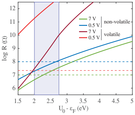
T(V,l) = exp{−(4 d_Si √(2m*)/(3ℏV))[(U0−ε)^{3/2} − q·(U0−ε−lV/d_Si)^{3/2}]} (WKB transmission with fitted U0−εF ∈ [2.00, 2.75] eV)
What do these tags mean?
- matches
- The paper's claim is directly supported by a theorem in the formal canon.
- supports
- The theorem supports part of the paper's argument, but the paper may add assumptions or extra steps.
- extends
- The paper goes beyond the formal theorem; the theorem is a base layer rather than the whole result.
- uses
- The paper appears to rely on the theorem as machinery.
- contradicts
- The paper's claim conflicts with a theorem or certificate in the canon.
- unclear
- Pith found a possible connection, but the passage is too broad, indirect, or ambiguous to say the theorem truly supports the claim.
Reference graph
Works this paper leans on
-
[1]
P. M. Morse and H. Feshbach , year=. Methods of Theoretical Physics, vol. 1 , publisher=
-
[2]
Johnson, K. L. and Kendall, K. and Roberts, A. D. , Journal =. Surface energy and contact of elastic solids , Volume =
-
[3]
Journal of Applied Physics , volume =
Lundström, Ingemar and Svensson, Christer , title =. Journal of Applied Physics , volume =. 1972 , month =. doi:10.1063/1.1661067 , url =
-
[4]
E. O. Kane , title =
-
[5]
Kharkats, Yu. I. , title =. Soviet Electrochemistry , year =
-
[6]
Quantum model for phonon-assisted tunnel ionization of deep levels in a semiconductor , author =. Physical Review B , volume =. 1982 , month =. doi:10.1103/PhysRevB.25.6406 , url =
-
[7]
A model for the field and temperature dependence of Shockley-Read-Hall lifetimes in silicon , journal =. 1992 , doi =
work page 1992
- [8]
-
[9]
Jiménez-Molinos, F. and Palma, A. and Gámiz, F. and Banqueri, J. and López-Villanueva, J. A. , title =. Journal of Applied Physics , volume =. 2001 , doi =
work page 2001
-
[10]
Modeling of anomalous SILC in flash memories based on tunneling at multiple defects , journal =. 2002 , issn =. doi:https://doi.org/10.1016/S0038-1101(02)00144-2 , author =
-
[11]
Larcher, L. , journal=. Statistical simulation of leakage currents in MOS and flash memory devices with a new multiphonon trap-assisted tunneling model , year=
-
[12]
K. A. Nasyrov and V. A. Gritsenko and Yu. N. Novikov and A. K. Zakharov and J. H. Lee and S. W. Choi and S. D. Chae , title =. JETP Letters , year =
-
[13]
Programmable Resistance Switching in Nanoscale Two-Terminal Devices , volume =
Jo, Sung Hyun and Kim, Kuk-Hwan and Lu, Wei , year =. Programmable Resistance Switching in Nanoscale Two-Terminal Devices , volume =. Nano Letters , publisher =
-
[14]
Nazarov, Yuli V. and Blanter, Yaroslav M. , year=. Quantum Transport: Introduction to Nanoscience , publisher=
-
[15]
Electrochemical metallization memories—fundamentals, applications, prospects , volume =
Valov, Ilia and Waser, Rainer and Jameson, John R and Kozicki, Michael N , year =. Electrochemical metallization memories—fundamentals, applications, prospects , volume =. Nanotechnology , publisher =
-
[16]
Nasyrov, K. A. and Gritsenko, V. A. , title =. Journal of Applied Physics , volume =. 2011 , month =
work page 2011
-
[17]
Liu, Qi and Sun, Jun and Lv, Hangbing and Long, Shibing and Yin, Kuibo and Wan, Neng and Li, Yingtao and Sun, Litao and Liu, Ming , year =. Real‐Time Observation on Dynamic Growth/Dissolution of Conductive Filaments in Oxide‐Electrolyte‐Based ReRAM , volume =. Advanced Materials , publisher =
-
[18]
Observation of conducting filament growth in nanoscale resistive memories , volume =
Yang, Yuchao and Gao, Peng and Gaba, Siddharth and Chang, Ting and Pan, Xiaoqing and Lu, Wei , year =. Observation of conducting filament growth in nanoscale resistive memories , volume =. Nature Communications , publisher =
-
[19]
Bipolar Electrochemical Mechanism for Mass Transfer in Nanoionic Resistive Memories , volume =
Tian, Xuezeng and Yang, Shize and Zeng, Min and Wang, Lifen and Wei, Jiake and Xu, Zhi and Wang, Wenlong and Bai, Xuedong , year =. Bipolar Electrochemical Mechanism for Mass Transfer in Nanoionic Resistive Memories , volume =. Advanced Materials , publisher =
-
[20]
Yang, Yuchao and Gao, Peng and Li, Linze and Pan, Xiaoqing and Tappertzhofen, Stefan and Choi, ShinHyun and Waser, Rainer and Valov, Ilia and Lu, Wei D. , year =. Electrochemical dynamics of nanoscale metallic inclusions in dielectrics , volume =. Nature Communications , publisher =
-
[21]
Wang, Zhongrui and Joshi, Saumil and Savel’ev, Sergey E. and Jiang, Hao and Midya, Rivu and Lin, Peng and Hu, Miao and Ge, Ning and Strachan, John Paul and Li, Zhiyong and Wu, Qing and Barnell, Mark and Li, Geng-Lin and Xin, Huolin L. and Williams, R. Stanley and Xia, Qiangfei and Yang, J. Joshua , year =. Memristors with diffusive dynamics as synaptic em...
-
[22]
Lanza, Mario and Celano, Umberto and Miao, Feng , year =. Nanoscale characterization of resistive switching using advanced conductive atomic force microscopy based setups , volume =. Journal of Electroceramics , publisher =
-
[23]
Probing nanoscale oxygen ion motion in memristive systems , volume =
Yang, Yuchao and Zhang, Xiaoxian and Qin, Liang and Zeng, Qibin and Qiu, Xiaohui and Huang, Ru , year =. Probing nanoscale oxygen ion motion in memristive systems , volume =. Nature Communications , publisher =
-
[24]
Nanometer‐Scale Phase Transformation Determines Threshold and Memory Switching Mechanism , volume =
Chae, Byeong‐Gyu and Seol, Jae‐Bok and Song, Jeong‐Hwan and Baek, Kyungjoon and Oh, Sang‐Ho and Hwang, Hyunsang and Park, Chan‐Gyung , year =. Nanometer‐Scale Phase Transformation Determines Threshold and Memory Switching Mechanism , volume =. Advanced Materials , publisher =
-
[25]
Probing memristive switching in nanoionic devices , volume =
Yang, Yuchao and Huang, Ru , year =. Probing memristive switching in nanoionic devices , volume =. Nature Electronics , publisher =
-
[26]
Ielmini, Daniele and Wong, H.-S. Philip , year =. In-memory computing with resistive switching devices , volume =. Nature Electronics , publisher =
-
[27]
del Valle, Javier and Ramírez, Juan Gabriel and Rozenberg, Marcelo J. and Schuller, Ivan K. , year =. Challenges in materials and devices for resistive-switching-based neuromorphic computing , volume =. Journal of Applied Physics , publisher =
-
[28]
Xia, Qiangfei and Yang, J. Joshua , year =. Memristive crossbar arrays for brain-inspired computing , volume =. Nature Materials , publisher =
-
[29]
and Qiu, Qinru and Williams, R
Wang, Zhongrui and Li, Can and Song, Wenhao and Rao, Mingyi and Belkin, Daniel and Li, Yunning and Yan, Peng and Jiang, Hao and Lin, Peng and Hu, Miao and Strachan, John Paul and Ge, Ning and Barnell, Mark and Wu, Qing and Barto, Andrew G. and Qiu, Qinru and Williams, R. Stanley and Xia, Qiangfei and Yang, J. Joshua , year =. Reinforcement learning with a...
-
[30]
Ang, D. S. and Zhou, Y. and Yew, K. S. and Berco, D. , year =. On the area scalability of valence-change memristors for neuromorphic computing , volume =. Applied Physics Letters , publisher =
-
[31]
Wang, J. J. and Yu, Q. and Hu, S. G. and Liu, Yanchen and Guo, Rui and Chen, T. P. and Yin, Y. and Liu, Y. , year =. Winner-takes-all mechanism realized by memristive neural network , volume =. Applied Physics Letters , publisher =
-
[32]
Zhang, Yang and Wang, Zhongrui and Zhu, Jiadi and Yang, Yuchao and Rao, Mingyi and Song, Wenhao and Zhuo, Ye and Zhang, Xumeng and Cui, Menglin and Shen, Linlin and Huang, Ru and Joshua Yang, J. , year =. Brain-inspired computing with memristors: Challenges in devices, circuits, and systems , volume =. Applied Physics Reviews , publisher =
-
[33]
Qi, Meng and Cao, Shuo and Yang, Liu and You, Qi and Shi, Libin and Wu, Zhiying , year =. Uniform multilevel switching of graphene oxide-based RRAM achieved by embedding with gold nanoparticles for image pattern recognition , volume =. Applied Physics Letters , publisher =
-
[34]
Design of defect-chemical properties and device performance in memristive systems , volume =
L\". Design of defect-chemical properties and device performance in memristive systems , volume =. Science Advances , publisher =
-
[35]
Yeon, Hanwool and Lin, Peng and Choi, Chanyeol and Tan, Scott H. and Park, Yongmo and Lee, Doyoon and Lee, Jaeyong and Xu, Feng and Gao, Bin and Wu, Huaqiang and Qian, He and Nie, Yifan and Kim, Seyoung and Kim, Jeehwan , year =. Alloying conducting channels for reliable neuromorphic computing , volume =. Nature Nanotechnology , publisher =
-
[36]
Ielmini, D. and Wang, Z. and Liu, Y. , year =. Brain-inspired computing via memory device physics , volume =. APL Materials , publisher =
-
[37]
Leng, Kangmin and Yu, Xinyue and Ma, Zhongyuan and Li, Wei and Xu, Jun and Xu, Ling and Chen, Kunji , year =. Artificial synapse arrays based on SiOx/TiOx memristive crossbar with high uniformity for neuromorphic computing , volume =. Applied Physics Letters , publisher =
-
[38]
Kang, Jaehyun and Kim, Taeyoon and Hu, Suman and Kim, Jaewook and Kwak, Joon Young and Park, Jongkil and Park, Jong Keuk and Kim, Inho and Lee, Suyoun and Kim, Sangbum and Jeong, YeonJoo , year =. Cluster-type analogue memristor by engineering redox dynamics for high-performance neuromorphic computing , volume =. Nature Communications , publisher =
-
[39]
Xiao, Yongyue and Jiang, Bei and Zhang, Zihao and Ke, Shanwu and Jin, Yaoyao and Wen, Xin and Ye, Cong , year =. A review of memristor: material and structure design, device performance, applications and prospects , volume =. Science and Technology of Advanced Materials , publisher =
-
[40]
Aguirre, Fernando and Sebastian, Abu and Le Gallo, Manuel and Song, Wenhao and Wang, Tong and Yang, J. Joshua and Lu, Wei and Chang, Meng-Fan and Ielmini, Daniele and Yang, Yuchao and Mehonic, Adnan and Kenyon, Anthony and Villena, Marco A. and Roldán, Juan B. and Wu, Yuting and Hsu, Hung-Hsi and Raghavan, Nagarajan and Suñé, Jordi and Miranda, Enrique an...
-
[41]
Samsonova, A. and Yegiyan, S. and Klimenko, O. and Antonov, V. N. and Paradezhenko, G. and Prodan, D. and Pervishko, A. and Yudin, D. and Brilliantov, N. , year =. Fabrication and study of the p-Si/a-Si/Ag memristor crossbar array , volume =. Zh.Eksp.Teor.Fiz. , publisher =
-
[42]
Zhang, Guobin and Wang, Zijian and Fan, Xuemeng and Wang, Zhen and Li, Pengtao and Luo, Qi and Gao, Dawei and Wan, Qing and Zhang, Yishu , year =. Self-rectifying memristors with high rectification ratio and dynamic linearity for in-memory computing , volume =. Applied Physics Letters , publisher =. doi:10.1063/5.0225833 , number =
-
[43]
Samsonova, A. and Sukhomlin, D. and Klimenko, O. and Brilliantov, N. and Antonov, V. N. , year =. Study of Ti/TiO2/Ti selector for the memristive crossbar array , volume =. Journal of Applied Physics , publisher =. doi:10.1063/5.0269515 , number =
-
[44]
M. Abramowitz and I. A. Stegun , year=. Handbook of Mathematical Functions. , publisher=
discussion (0)
Sign in with ORCID, Apple, or X to comment. Anyone can read and Pith papers without signing in.