Deterministic Single-Photon Emitter Arrays in Hexagonal Boron Nitride by Carbon-Assisted Focused Ion Beam Engineering
Pith reviewed 2026-06-27 08:33 UTC · model grok-4.3
The pith
A three-step process of Ga ion milling, carbon deposition and annealing creates deterministic single-photon emitter arrays in hBN at 89% site yield.
A machine-rendered reading of the paper's core claim, the machinery that carries it, and where it could break.
Core claim
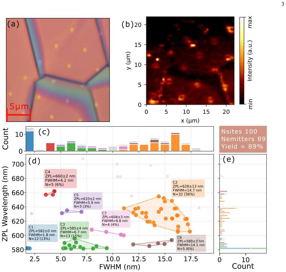
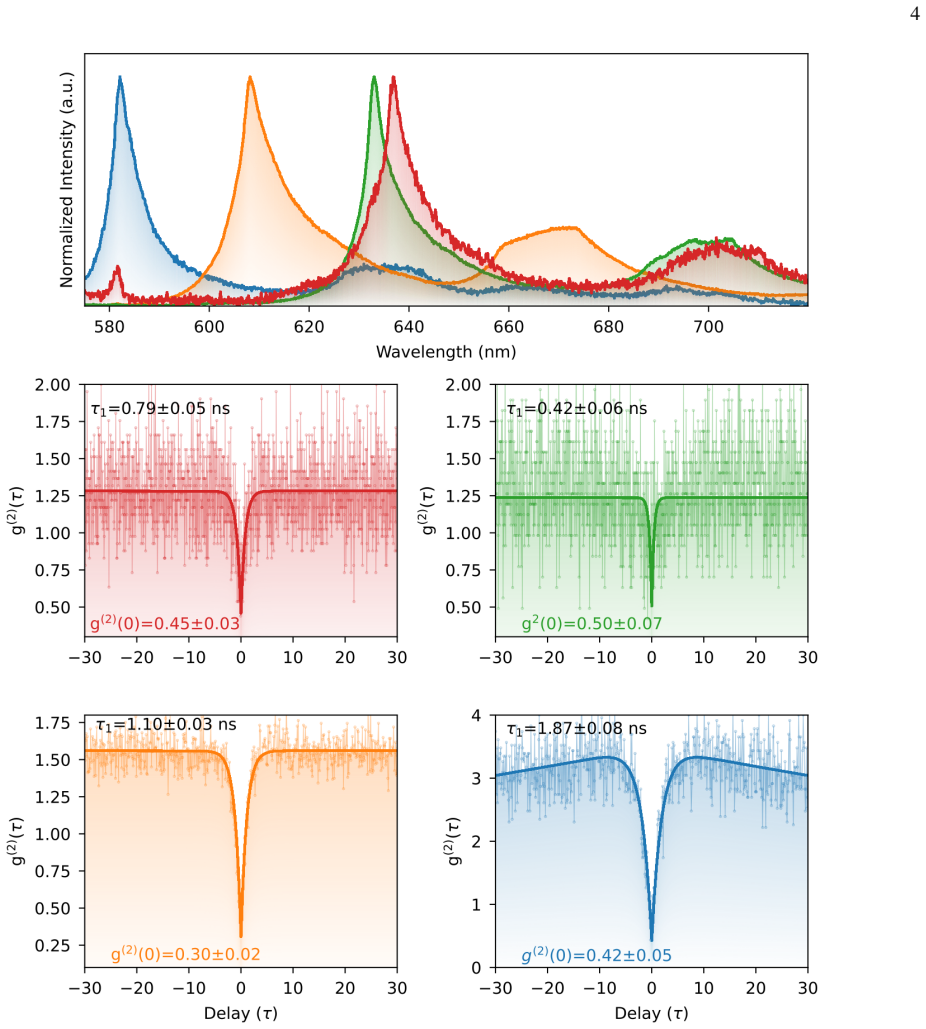
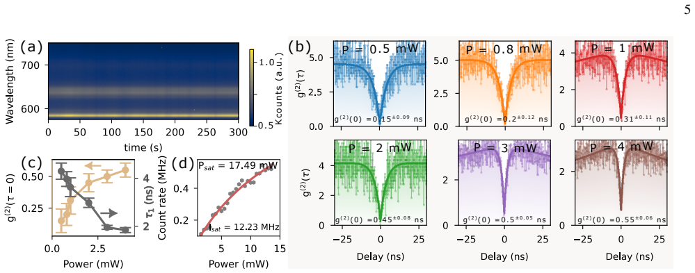
The synergistic combination of site-selective gallium focused ion beam milling, nanoscale conformal carbon deposition over the patterned regions, and subsequent thermal annealing generates spatially controlled single-photon emitter arrays in hexagonal boron nitride with a site-correlated emitter yield of approximately 89 percent across 100 fabrication sites, where the best emitters exhibit g^{(2)}(0) of 0.15 plus or minus 0.09 and pronounced three-level dynamics.
What carries the argument
The three-step process of Ga-ion milling, selective carbon engineering, and thermal annealing that produces site-controlled emitters.
Load-bearing premise
The high site yield and single-photon character result specifically from the carbon-assisted process rather than random background defects or uncontrolled variables in the hBN.
What would settle it
Control samples that receive only ion milling and annealing without the carbon deposition step showing comparable site yields near 89 percent and g squared values near 0.15 would indicate the carbon step is not required.
Figures
read the original abstract
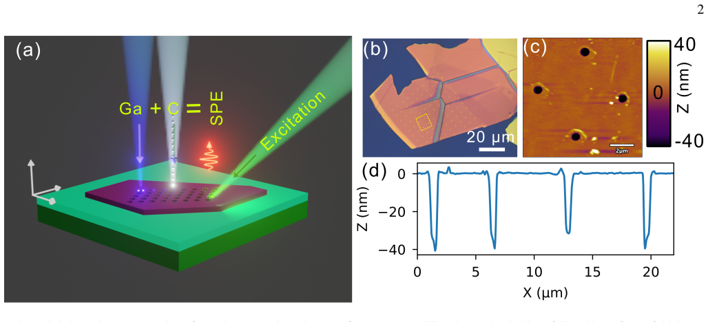
The realization of on-chip photonic circuits requires scalable and deterministic single-photon emitters (SPEs) at room temperature, which remain a challenge in van der Waals materials. In this work, we report a novel three-step fabrication process for the generation of spatially controlled SPE arrays in hexagonal boron nitride (hBN). The process comprises site-selective gallium (Ga) focused ion beam milling, nanoscale conformal carbon deposition over the patterned regions, and subsequent thermal annealing. The synergistic combination of these steps resulted in a site-correlated emitter yield of ($\sim 89\%$) across 100 fabrication sites. Second-order autocorrelation measurements revealed pronounced three-level emitter dynamics where the best emitters exhibited high purity ($g^{(2)}(0)=0.15 \pm 0.09$).To the best of our knowledge, this is the first lithography-free, direct-write approach combining Ga-ion milling, selective carbon engineering, and thermal annealing to deterministically generate \hBN{} \SPE{}s. The reproducibility of the method is validated across multiple independently fabricated samples. These results establish a scalable, lithography-free pathway toward on-demand SPE arrays relevant to integrated quantum photonics.
Editorial analysis
A structured set of objections, weighed in public.
Referee Report
Summary. The paper claims that a three-step, lithography-free process—site-selective Ga focused ion beam milling, nanoscale conformal carbon deposition, and thermal annealing—produces deterministic single-photon emitter arrays in hBN with a site-correlated yield of ~89% across 100 fabrication sites. The best emitters show three-level dynamics and high purity with g^{(2)}(0) = 0.15 ± 0.09, and the method is reported to be reproducible across multiple independently fabricated samples.
Significance. If the attribution of the high yield to the specific process holds after controls, the work would provide a scalable direct-write route to room-temperature SPE arrays in a van der Waals material, relevant to integrated quantum photonics. The reported yield and autocorrelation values are concrete and the reproducibility claim across samples is a positive feature.
major comments (1)
- [Abstract/Results] Abstract and Results: The central claim that the ~89% site-correlated yield is produced by the synergistic Ga-FIB + carbon + anneal sequence requires isolation from native defects. No quantitative emitter-density comparison is reported between the patterned sites and adjacent unprocessed regions of the same flakes, nor any pre-fabrication survey of the starting material; without these baselines the causal attribution to the carbon-assisted process remains unestablished.
minor comments (1)
- [Abstract] The abstract states that second-order autocorrelation measurements revealed 'pronounced three-level emitter dynamics' but supplies no details on the fitting model, background subtraction, or how many emitters were measured to obtain the quoted g^{(2)}(0) value and uncertainty.
Simulated Author's Rebuttal
We thank the referee for the constructive review. We respond point-by-point to the major comment below.
read point-by-point responses
-
Referee: [Abstract/Results] Abstract and Results: The central claim that the ~89% site-correlated yield is produced by the synergistic Ga-FIB + carbon + anneal sequence requires isolation from native defects. No quantitative emitter-density comparison is reported between the patterned sites and adjacent unprocessed regions of the same flakes, nor any pre-fabrication survey of the starting material; without these baselines the causal attribution to the carbon-assisted process remains unestablished.
Authors: The referee is correct that the manuscript does not report quantitative emitter-density measurements comparing processed sites to adjacent unprocessed regions of the same flakes, nor pre-fabrication surveys of native defect density. The reported 89% figure is a site-correlated yield (fraction of the 100 targeted sites that produced emitters), with spatial localization to the milled and carbon-deposited areas and reproducibility across independent samples. While this spatial selectivity and the three-level dynamics provide supporting evidence for the process, the absence of the requested baselines leaves the causal attribution less firmly established than claimed. We will add such comparative density data in the revised manuscript. revision: yes
Circularity Check
No derivation chain or fitted parameters present
full rationale
This is an experimental fabrication and characterization paper reporting a three-step process (Ga FIB milling, carbon deposition, annealing), site yields (~89%), and g(2)(0) measurements. No equations, derivations, ansatzes, fitted parameters, or self-citation load-bearing uniqueness theorems appear in the provided text or abstract. All central claims rest on direct experimental observations rather than any reduction of outputs to inputs by construction. The absence of a mathematical derivation chain makes circularity analysis inapplicable; the paper is self-contained against external benchmarks in the sense required by the rules.
Axiom & Free-Parameter Ledger
Reference graph
Works this paper leans on
-
[1]
V ogl, V
T. V ogl, V . Iv´ady, I. J. Luxmoore, and H. L. Stern, 2D Materials 13, 023001 (2026)
2026
-
[2]
Scarani, H
V . Scarani, H. Bechmann-Pasquinucci, N. J. Cerf, M. Du ˇsek, N. L ¨utkenhaus, and M. Peev, Reviews of Modern Physics81, 1301–1350 (2009)
2009
-
[3]
Mehic, M
M. Mehic, M. Niemiec, S. Rass, J. Ma, M. Peev, A. Aguado, V . Martin, S. Schauer, A. Poppe, C. Pacher, and M. V oznak, ACM Computing Surveys53, 1–41 (2020)
2020
-
[4]
A. K. Singh, P. Sharma, K. K. Mandal, L. Eswaramoorthy, and A. Kumar, From atomic defects to integrated photonics: A per- spective on solid-state quantum light sources (2025)
2025
-
[5]
Reviews of Modern Physics89(3), 035002 (2017) https://doi.org/10.1103/RevModPhys.89.035002
C. Degen, F. Reinhard, and P. Cappellaro, Reviews of Modern Physics89, 10.1103/revmodphys.89.035002 (2017)
work page internal anchor Pith review doi:10.1103/revmodphys.89.035002 2017
-
[6]
S. Vaidya, X. Gao, S. Dikshit, I. Aharonovich, and T. Li, Advances in Physics: X8, 10.1080/23746149.2023.2206049 (2023)
-
[7]
R. Rizzato, M. Schalk, S. Mohr, J. C. Hermann, J. P. Lei- bold, F. Bruckmaier, G. Salvitti, C. Qian, P. Ji, G. V . As- takhov, U. Kentsch, M. Helm, A. V . Stier, J. J. Finley, and D. B. Bucher, Nature Communications14, 10.1038/s41467- 023-40473-w (2023)
-
[8]
S. Hou, H. Hu, M. Xu, J. Zhang, H. Xiao, Z. Liu, W. Xing, X. Liu, S. You, B. Liu, Y . Zhang, J. Yu, Z. Xie, X. He, J. Zhang, and Y . Hao, Advanced Optical Materials13, 10.1002/adom.202500693 (2025)
-
[9]
Aharonovich, D
I. Aharonovich, D. Englund, and M. Toth, Nature Photonics10, 631–641 (2016)
2016
-
[10]
Daggett, C
E. Daggett, C. M. Lange, B. Windt, A. Danageozian, A. Senichev, J. A. Monta ˜n`a-L´opez, Chanchal, K. Barua, X. Gao, Z. Zheng, V . Kizhake Veetil, S. Biswas, J. M. Peter- son, N. Liu, C. Hong, T. Odom, M. Pelton, T. Li, J. Vu ˇckovi´c, V . M. Shalaev, A. Boltasseva, S. E. Economou, J. D. Hood, V . Walther, R. Trivedi, and L. Huang, Nature Reviews Materi- ...
2026
-
[11]
A. K. Singh, Utkarsh, P. Tieben, K. K. Mandal, B. Kumar, R. Vij, A. Majumder, I. Shyam, S. Kumar, K. Watanabe, T. Taniguchi, V . G. Achanta, A. W. Schell, and A. Kumar, Advanced Materials Interfaces12, 10.1002/admi.202500071 (2025)
-
[12]
Aharonovich, D
I. Aharonovich, D. Englund, and M. Toth, Nature photonics10, 631 (2016)
2016
-
[13]
A. Kumar, C. Cholsuk, A. Zand, M. N. Mishuk, T. Matthes, F. Eilenberger, S. Suwanna, and T. V ogl, APL Materials11, 10.1063/5.0147560 (2023)
-
[14]
S. L. Ahmed, L. Harsch, C. Imre, I. Karapatzakis, L. Kussi, J. Resch, M. Schrodin, I. H ¨ausler, T. Wagner, C. T. Koch, C. S ¨urgers, and W. Wernsdorfer, ACS Nano19, 36302–36312 (2025)
2025
-
[15]
T. T. Tran, C. Elbadawi, D. Totonjian, C. J. Lobo, G. Grosso, H. Moon, D. R. Englund, M. J. Ford, I. Aharonovich, and M. Toth, ACS nano10, 7331 (2016)
2016
-
[16]
M. Luo, J. Ge, P. Huang, Y . Yu, I. C. Seo, K. Lu, H. Sun, J. K. Tan, B. K. Tay, S. Kim, W. Gao, H. Li, and D. Nam, Nature Communications16, 10.1038/s41467-025-66314-6 (2025)
-
[17]
S. Park, K. H. Park, Y . Kim, and Y . D. Kim, Current Applied Physics89, 53–59 (2026)
2026
-
[18]
A. Sajid, J. R. Reimers, and M. J. Ford, Physical Review B97, 10.1103/physrevb.97.064101 (2018)
-
[19]
L. Eswaramoorthy, P. Sharma, B. Kumar, A. Anand, A. K. Singh, S. Mokkapati, and A. Kumar, arXiv preprint arXiv:2510.26637 (2025)
arXiv 2025
-
[20]
Eswaramoorthy, P
L. Eswaramoorthy, P. Sharma, B. Kumar, A. A. V . S, A. K. Singh, K. K. Mandal, S. Mokkapati, and A. Kumar, Physica Scripta101, 045513 (2026)
2026
-
[21]
G. Grosso, H. Moon, B. Lienhard, S. Ali, D. K. Efetov, M. M. Furchi, P. Jarillo-Herrero, M. J. Ford, I. Aharonovich, and D. Englund, Nature Communications8, 10.1038/s41467-017- 00810-2 (2017)
-
[22]
J. E. Fr ¨och, L. P. Spencer, M. Kianinia, D. D. Totonjian, M. Nguyen, A. Gottscholl, V . Dyakonov, M. Toth, S. Kim, and I. Aharonovich, Nano Letters21, 6549–6555 (2021)
2021
-
[23]
G. Venturi, S. Chiodini, N. Melchioni, E. Janzen, J. H. Edgar, C. Ronning, and A. Ambrosio, Laser Photonics Reviews18, 10.1002/lpor.202300973 (2024)
-
[24]
T. W. Tang, R. Ritika, M. Tamtaji, H. Liu, Y . Hu, Z. Liu, P. R. Galligan, M. Xu, J. Shen, J. Wang, J. You, Y . Li, G. Chen, I. Aharonovich, and Z. Luo, ACS Nano19, 8509–8519 (2025)
2025
-
[25]
B. Chakraborty, P. Joshi, S. Singla, G. Morales, D. Sharma, S. Makineni, K. Watanabe, T. Taniguchi, S. Sarkar, and C. Dreyer, Research Square preprint 10.21203/rs.3.rs- 5579262/v1 (2025)
-
[26]
A. Zobelli, C. P. Ewels, A. Gloter, and G. Seifert, Physical Re- view B75, 10.1103/physrevb.75.094104 (2007)
-
[27]
Miao, Physical Review A95, 10.1103/phys- reva.95.012103 (2017)
L. Weston, D. Wickramaratne, M. Mackoit, A. Alkauskas, and C. G. Van de Walle, Physical Review B97, 10.1103/phys- revb.97.214104 (2018)
-
[28]
F. A. Khaleel and S. K. Tawfeeq, International Journal of Nu- merical Modelling: Electronic Networks, Devices and Fields 35, 10.1002/jnm.3013 (2022)
-
[29]
Kumar, P
B. Kumar, P. S. Choubey, and B. S. Bhaktha, The European Physical Journal Special Topics231, 781 (2022)
2022
-
[30]
A. K. Singh, K. K. Mandal, Y . Gupta, A. Anand VS, L. Eswaramoorthy, B. Kumar, A. Kala, S. Dixit, V . G. Achanta, and A. Kumar, Physical Review Applied19, 044012 (2023)
2023
-
[31]
Kumar Mandal, Y
K. Kumar Mandal, Y . Gupta, B. Kumar, M. Sohoni, A. Venu Gopal, and A. Kumar, Journal of applied physics133 (2023)
2023
-
[32]
Sharma, B
P. Sharma, B. Kumar, N. R. Sahoo, and A. Kumar, Sensors and Actuators A: Physical378, 115681 (2024)
2024
-
[33]
Kumar, A
B. Kumar, A. K. Singh, K. K. Mandal, P. Sharma, N. R. Sa- hoo, and A. Kumar, Journal of Physics D: Applied Physics56, 425105 (2023)
2023
discussion (0)
Sign in with ORCID, Apple, or X to comment. Anyone can read and Pith papers without signing in.