Strain- and Electric-Field-Tunable Valley Polarization in Mo0.75V0.25Te2(Mo3VTe8) for Valleytronic Application
Pith reviewed 2026-06-26 16:40 UTC · model grok-4.3
The pith
V alloying in MoTe2 monolayer creates spontaneous valley polarization tunable by electric field and strain up to 160 meV.
A machine-rendered reading of the paper's core claim, the machinery that carries it, and where it could break.
Core claim
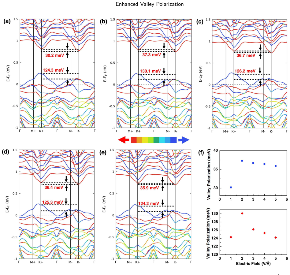
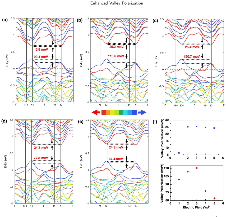
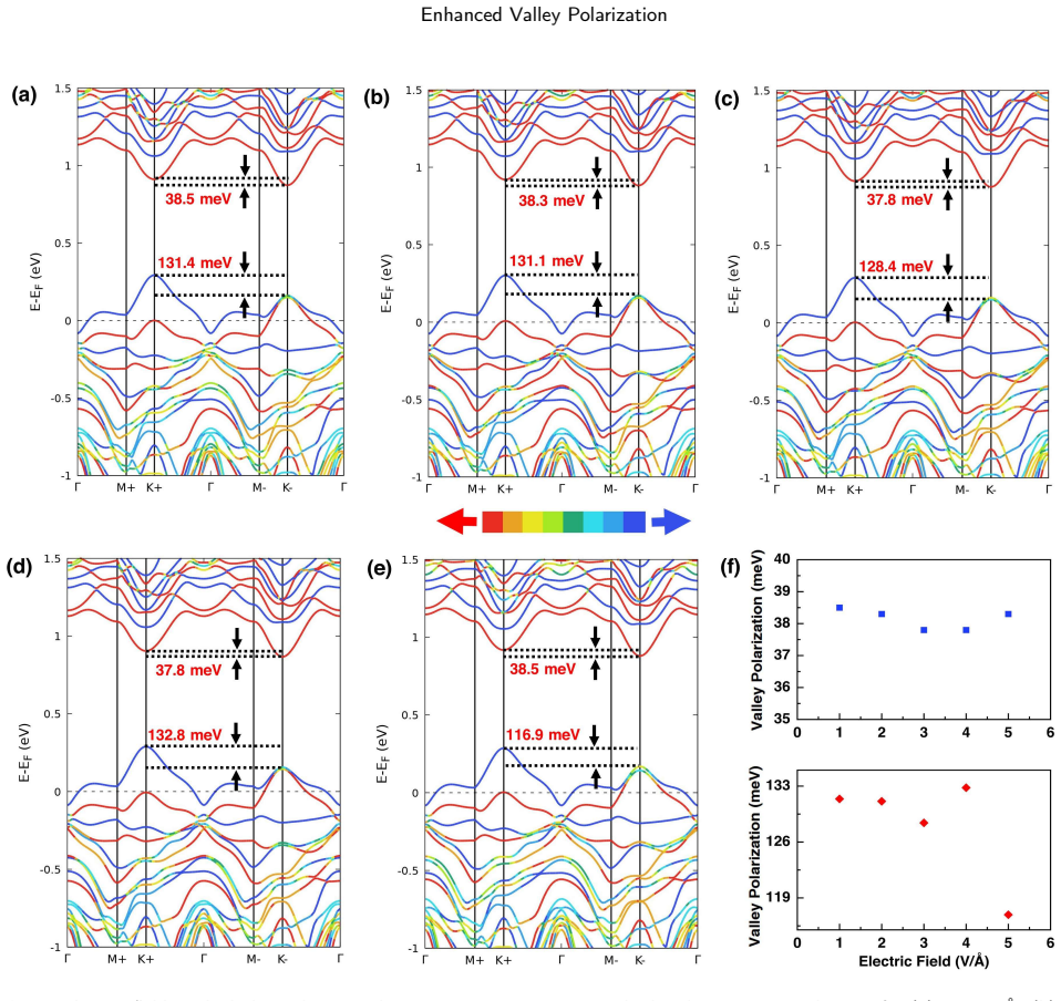
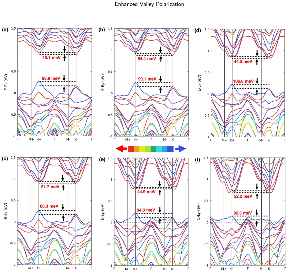
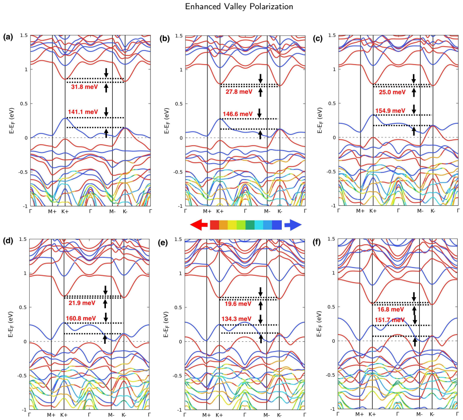
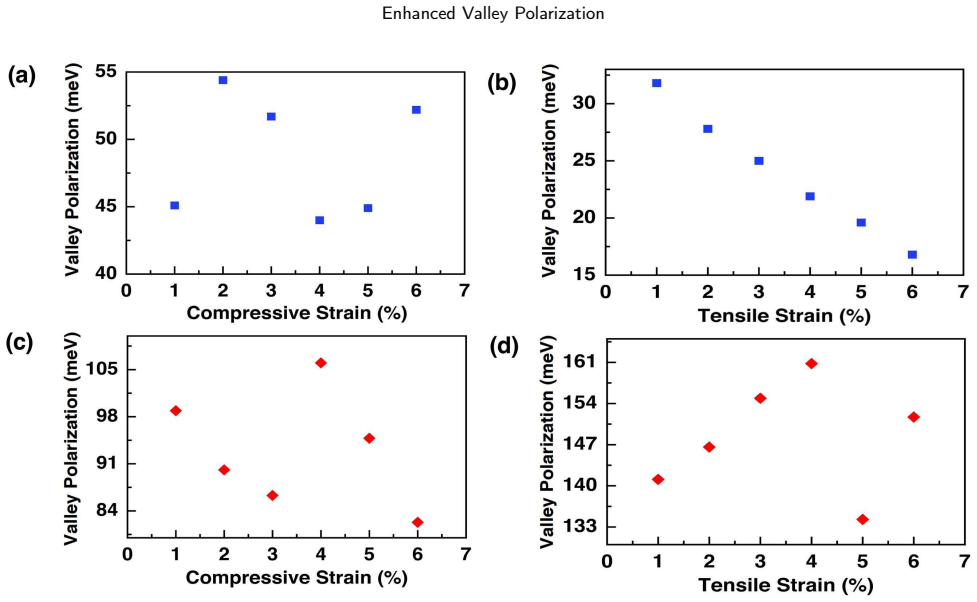
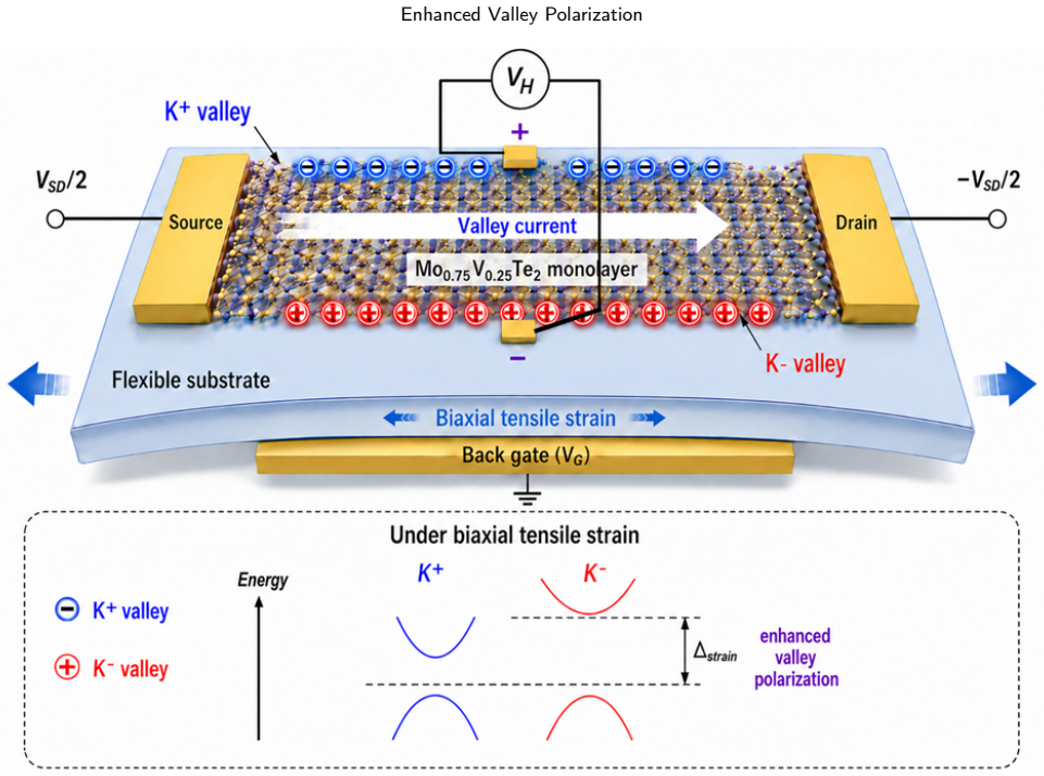
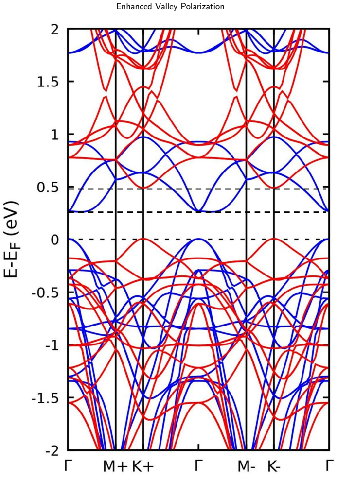
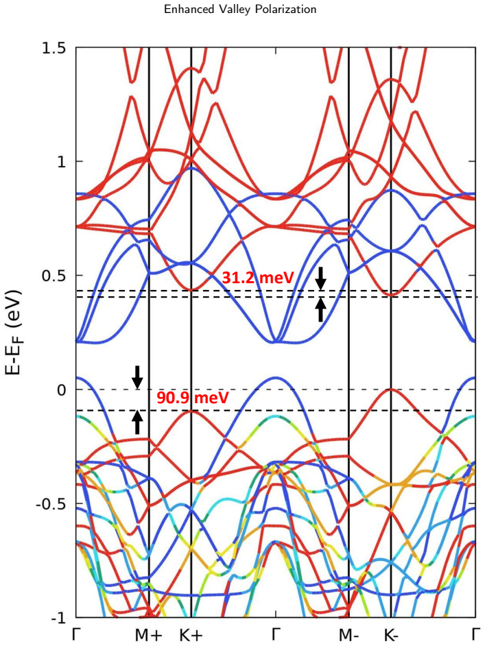
Substitutional alloying of MoTe2 with 25 percent V produces an energetically and dynamically stable monolayer that exhibits spontaneous valley polarization of 37.3 meV in the conduction band and 78.2 meV in the valence band due to magnetic exchange interaction combined with spin-orbit coupling; this polarization is enhanced to a maximum of 132.8 meV by a transverse electric field and to 160.8 meV by biaxial tensile strain.
What carries the argument
Magnetic exchange interaction from V substitution together with spin-orbit coupling, which together lift the valley degeneracy at the K and K' points.
If this is right
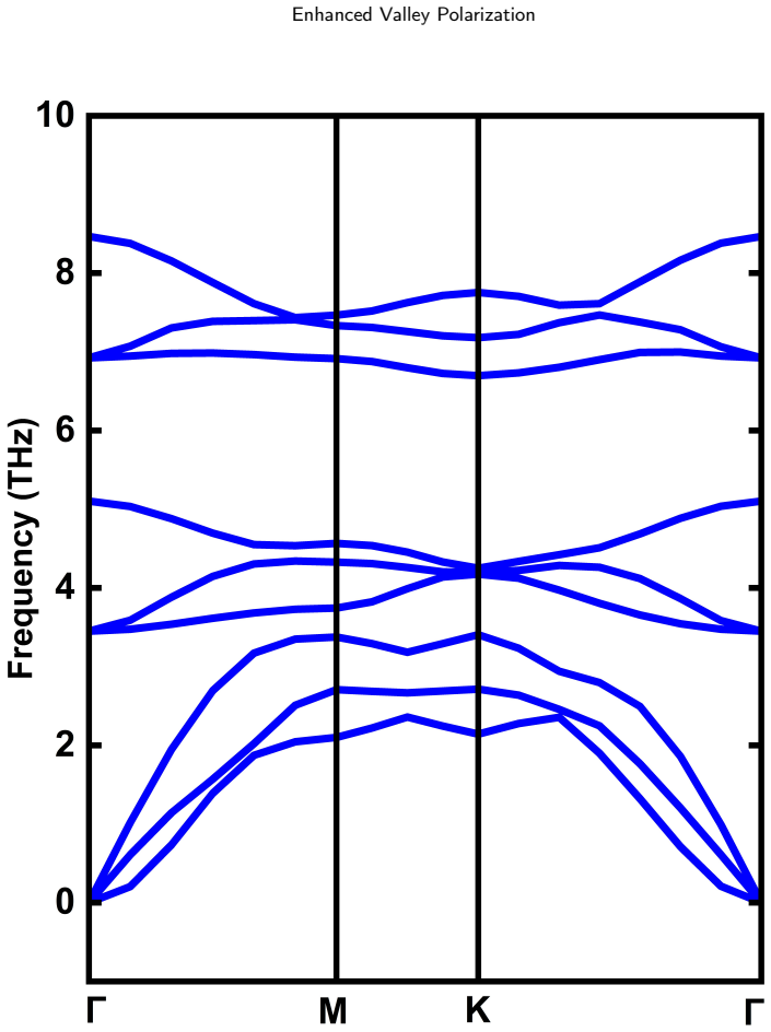
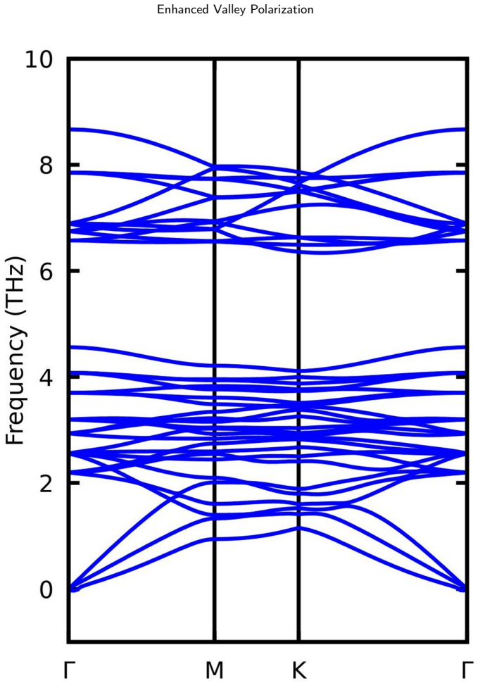
- The alloyed monolayer is energetically and dynamically stable owing to the absence of imaginary phonon modes.
- A transverse electric field along the c axis produces a maximum valence-band valley splitting of 132.8 meV.
- Biaxial tensile strain increases the valence-band valley splitting to 160.8 meV.
- The conduction-band valley splitting reaches a maximum of 54.4 meV under 2 percent biaxial compressive strain.
- The material offers a platform for tunable valleytronic devices such as transistors and sensors.
Where Pith is reading between the lines
- Similar vanadium or other magnetic-atom alloying could induce valley polarization in additional transition-metal dichalcogenides without requiring external magnetic fields.
- Fabrication and optical or transport measurements on actual Mo0.75V0.25Te2 samples could test whether the calculated splittings appear in measurable valleytronic signals.
- Stacking the alloy with other two-dimensional layers might introduce extra knobs for controlling the valley splitting through proximity effects.
Load-bearing premise
The density functional theory calculations correctly capture the magnetic exchange interaction and spin-orbit coupling that lift valley degeneracy, and the alloy remains stable at 25 percent vanadium substitution.
What would settle it
An experiment that finds no energy difference between the K and K' valleys or detects imaginary phonon modes in the Mo0.75V0.25Te2 monolayer would disprove the predicted spontaneous polarization and structural stability.
Figures
read the original abstract
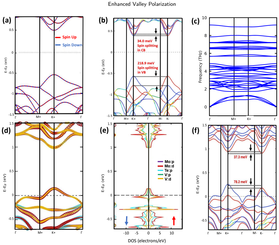
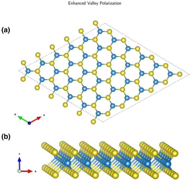
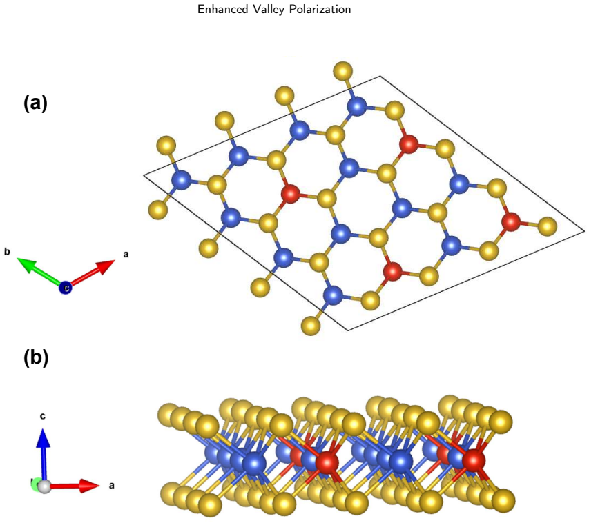
Valley polarization in 2D TMDs is promising for low-power valleytronic and spin-valley information processing, but time-reversal symmetry in pristine nonmagnetic TMDs keeps the K+ and K- valleys degenerate, limiting device applications. In this work, we investigated the structural stability, electronic properties, and tunable valley polarization of V-alloyed MoTe2 monolayer, Mo0.75V0.25Te2, using first-principles density functional theory (DFT) calculations. Substitutional alloying of MoTe2 with V introduced magnetic exchange interaction, which, together with spin-orbit coupling (SOC), lifted the valley degeneracy at the unequal valleys. The alloyed structure was found to be energetically and dynamically stable due to the absence of imaginary phonon modes. In pristine MoTe2, SOC produced spin splittings of 34.0 meV and 218.9 meV in the conduction bands and valence bands, respectively, but no valley polarization was observed. In contrast, Mo0.75V0.25Te2 exhibited spontaneous valley polarization of 37.3 meV in the conduction band and 78.2 meV in the valence band. The valley polarization was further enhanced by external electric fields and biaxial strain. A transverse electric field along the crystal c axis produced the maximum valley splitting of 132.8 meV in the valence band, whereas biaxial tensile strain increased the valence band valley splitting up to 160.8 meV. The maximum conduction band valley splitting reached 54.4 meV under 2% biaxial compressive strain. These results demonstrated that V alloying, combined with electric-field and strain engineering, provides an effective strategy for achieving large and tunable valley polarization in MoTe2. Thus, Mo0.75V0.25Te2 can be considered a promising 2D platform for tunable valleytronic device applications, such as transistors and sensors.
Editorial analysis
A structured set of objections, weighed in public.
Referee Report
Summary. The manuscript uses first-principles DFT to study the Mo0.75V0.25Te2 (Mo3VTe8) monolayer, claiming that 25% V substitution induces spontaneous valley polarization (37.3 meV conduction band, 78.2 meV valence band) via magnetic exchange plus SOC, that the structure is dynamically stable (no imaginary phonons), and that the splitting can be further tuned to 132.8 meV (E-field) or 160.8 meV (biaxial tensile strain) in the valence band.
Significance. If the numerical results are reproducible, the work would demonstrate a concrete materials-design route to spontaneous and externally tunable valley polarization in a 2D TMD, which is of interest for valleytronic devices. The manuscript does not, however, supply the computational parameters required to judge whether the reported splittings are robust.
major comments (3)
- [Abstract, §2] Abstract and §2 (Computational Methods): No exchange-correlation functional, k-mesh density, plane-wave cutoff, Hubbard U (if any) for V, or supercell construction details are provided. Without these parameters the central claims of 37.3 meV and 78.2 meV valley splittings cannot be reproduced or assessed for convergence or supercell-ordering artifacts.
- [Abstract] Abstract (phonon stability paragraph): The assertion of dynamical stability rests on “absence of imaginary phonon modes,” yet no q-mesh, supercell size for the phonon calculation, or convergence criteria are stated. This directly affects the reliability of the structural-stability prerequisite for the electronic results.
- [Abstract] Abstract (electric-field and strain results): The maximum valence-band splittings of 132.8 meV (E-field) and 160.8 meV (strain) are reported as quantitative outcomes, but the same missing methodological details prevent evaluation of whether these enhancements are numerically converged or sensitive to the chosen field/strain implementation.
minor comments (1)
- [Title, Abstract] The notation “Mo0.75V0.25Te2(Mo3VTe8)” in the title and abstract is redundant; a single consistent formula is sufficient.
Simulated Author's Rebuttal
We thank the referee for their careful review and for highlighting the importance of methodological transparency to ensure reproducibility. We have revised the manuscript to supply all requested computational parameters.
read point-by-point responses
-
Referee: [Abstract, §2] Abstract and §2 (Computational Methods): No exchange-correlation functional, k-mesh density, plane-wave cutoff, Hubbard U (if any) for V, or supercell construction details are provided. Without these parameters the central claims of 37.3 meV and 78.2 meV valley splittings cannot be reproduced or assessed for convergence or supercell-ordering artifacts.
Authors: We agree that these parameters are required for reproducibility. In the revised manuscript we have expanded §2 to report the exchange-correlation functional, k-point mesh, plane-wave cutoff, any Hubbard U applied to V, and the supercell construction used for the 25 % V substitution. These additions directly address the concern and permit independent verification of the reported valley splittings. revision: yes
-
Referee: [Abstract] Abstract (phonon stability paragraph): The assertion of dynamical stability rests on “absence of imaginary phonon modes,” yet no q-mesh, supercell size for the phonon calculation, or convergence criteria are stated. This directly affects the reliability of the structural-stability prerequisite for the electronic results.
Authors: We accept the referee’s point. The revised manuscript now specifies the q-mesh, supercell size, and convergence criteria employed in the phonon calculations, allowing readers to evaluate the dynamical stability claim. revision: yes
-
Referee: [Abstract] Abstract (electric-field and strain results): The maximum valence-band splittings of 132.8 meV (E-field) and 160.8 meV (strain) are reported as quantitative outcomes, but the same missing methodological details prevent evaluation of whether these enhancements are numerically converged or sensitive to the chosen field/strain implementation.
Authors: We agree that the same methodological details are needed to assess the electric-field and strain results. The revised manuscript includes the implementation details and convergence information for both the transverse electric field and biaxial strain calculations. revision: yes
Circularity Check
No circularity: valley splittings are direct DFT outputs with no reduction to fitted inputs or self-citations
full rationale
The paper computes spontaneous valley polarization (37.3 meV CB, 78.2 meV VB) and its tuning under E-field/strain directly via first-principles DFT on the Mo3VTe8 supercell, including SOC and magnetic exchange from V substitution. These quantities are reported as numerical results of the electronic-structure calculation rather than quantities obtained by fitting parameters to the target splittings, by algebraic reduction of earlier equations in the paper, or by load-bearing self-citations. No ansatz, uniqueness theorem, or renaming of known results is invoked; the derivation chain is therefore self-contained standard DFT and receives score 0.
Axiom & Free-Parameter Ledger
axioms (1)
- domain assumption Density functional theory with spin-orbit coupling and magnetic exchange accurately reproduces the valley splitting and structural stability of the V-alloyed monolayer.
Reference graph
Works this paper leans on
-
[1]
Criticalchallengesin the development of electronics based on two-dimensional transition metal dichalcogenides,
Y.Wang,S.Sarkar,H.Yan,andM.Chhowalla,“Criticalchallengesin the development of electronics based on two-dimensional transition metal dichalcogenides,”Nature Electronics, vol. 7, no. 8, pp. 638– 645, 2024
2024
-
[2]
Optoelectronic devices based on electrically tunable p–n diodes in a monolayer dichalcogenide,
B. W. Baugher, H. O. Churchill, Y. Yang, and P. Jarillo-Herrero, “Optoelectronic devices based on electrically tunable p–n diodes in a monolayer dichalcogenide,”Nature Nanotechnology, vol. 9, no. 4, pp. 262–267, 2014
2014
-
[3]
Excitonic devices withvanderwaalsheterostructures:valleytronicsmeetstwistronics,
A. Ciarrocchi, F. Tagarelli, A. Avsar, and A. Kis, “Excitonic devices withvanderwaalsheterostructures:valleytronicsmeetstwistronics,” Nature Reviews Materials, vol. 7, no. 6, pp. 449–464, 2022. Islam, Chowdhury, Nure-Alam-Dipu and Zubair:Preprint submitted to ElsevierPage 13 of 21 Enhanced Valley Polarization
2022
-
[4]
Electrically switchable chiral light-emitting transistor,
Y. Zhang, T. Oka, R. Suzuki, J. Ye, and Y. Iwasa, “Electrically switchable chiral light-emitting transistor,”Science, vol. 344, no. 6185, pp. 725–728, 2014
2014
-
[5]
Valleytronics in transition metal dichalcogenides materials,
Y. Liu, Y. Gao, S. Zhang, J. He, J. Yu, and Z. Liu, “Valleytronics in transition metal dichalcogenides materials,”Nano Research, vol. 12, no. 11, pp. 2695–2711, 2019
2019
-
[6]
Design of ion-implanted MOSFET’s with very small physical dimensions,
R.H.Dennard,F.H.Gaensslen,H.-N.Yu,V.L.Rideout,E.Bassous, and A. R. LeBlanc, “Design of ion-implanted MOSFET’s with very small physical dimensions,”IEEE Journal of Solid-State Circuits, vol. 9, no. 5, pp. 256–268, 2003
2003
-
[7]
IEEEInternationalElectronDevicesMeeting,
M.Horowitz,E.Alon,D.Patil,S.Naffziger,R.Kumar,andK.Bern- stein,“IEEEInternationalElectronDevicesMeeting,”IEDM Techni- cal Digest (Washington, DC 2005 Dec. 5-7, IEEE Group on Electron Devices) p, vol. 7, 2005
2005
-
[8]
Valleytronics inmergingDiraccones:All-electric-controlledvalleyfilter,valve,and universalreversiblelogicgate,
Y.S.Ang,S.A.Yang,C.Zhang,Z.Ma,andL.K.Ang,“Valleytronics inmergingDiraccones:All-electric-controlledvalleyfilter,valve,and universalreversiblelogicgate,”Physical Review B,vol.96,no.24,p. 245410, 2017
2017
-
[9]
Flo- quet valley-polarized quantum anomalous hall state in nonmagnetic heterobilayers,
F. Zhan, Z. Ning, L.-Y. Gan, B. Zheng, J. Fan, and R. Wang, “Flo- quet valley-polarized quantum anomalous hall state in nonmagnetic heterobilayers,”Phys. Rev. B, vol. 105, p. L081115, Feb 2022
2022
-
[10]
Light–valley interactions in 2D semiconductors,
K. F. Mak, D. Xiao, and J. Shan, “Light–valley interactions in 2D semiconductors,”Nature Photonics,vol.12,no.8,pp.451–460,2018
2018
-
[11]
All-optical ultrafast valley switching in two- dimensional materials,
N. Rana and G. Dixit, “All-optical ultrafast valley switching in two- dimensional materials,”Phys. Rev. Appl., vol. 19, p. 034056, Mar 2023
2023
-
[12]
Quantum-engineered devices based on 2D materials for next-generation information processing and storage,
A. Pal, S. Zhang, T. Chavan, K. Agashiwala, C.-H. Yeh, W. Cao, and K. Banerjee, “Quantum-engineered devices based on 2D materials for next-generation information processing and storage,”Advanced Materials, vol. 35, no. 27, p. 2109894, 2023
2023
-
[13]
Valleytronics in 2D materials,
J. R. Schaibley, H. Yu, G. Clark, P. Rivera, J. S. Ross, K. L. Seyler, W. Yao, and X. Xu, “Valleytronics in 2D materials,”Nature Reviews Materials, vol. 1, no. 11, p. 16055, 2016
2016
-
[14]
Valleytronics: opportunities, challenges, and paths forward,
S. A. Vitale, D. Nezich, J. O. Varghese, P. Kim, N. Gedik, P. Jarillo- Herrero, D. Xiao, and M. Rothschild, “Valleytronics: opportunities, challenges, and paths forward,”Small, vol. 14, no. 38, p. 1801483, 2018
2018
-
[15]
TuningvalleypolarizationinaWSe 2monolayerwithatinymagnetic field,
T. Smoleński, M. Goryca, M. Koperski, C. Faugeras, T. Kazimier- czuk, A. Bogucki, K. Nogajewski, P. Kossacki, and M. Potemski, “TuningvalleypolarizationinaWSe 2monolayerwithatinymagnetic field,”Physical Review X, vol. 6, no. 2, p. 021024, 2016
2016
-
[16]
Enhancedvalleysplittinginmono- layerWSe 2 duetomagneticexchangefield,
C. Zhao, T. Norden, P. Zhang, P. Zhao, Y. Cheng, F. Sun, J. P. Parry, P.Taheri,J.Wang,Y.Yanget al.,“Enhancedvalleysplittinginmono- layerWSe 2 duetomagneticexchangefield,”Nature Nanotechnology, vol. 12, no. 8, pp. 757–762, 2017
2017
-
[17]
ManipulationofvalleypseudospininWSe 2/CrI3 heterostructuresby the magnetic proximity effect,
T. Hu, G. Zhao, H. Gao, Y. Wu, J. Hong, A. Stroppa, and W. Ren, “ManipulationofvalleypseudospininWSe 2/CrI3 heterostructuresby the magnetic proximity effect,”Physical Review B, vol. 101, no. 12, p. 125401, 2020
2020
-
[18]
Optical manipulation of valley pseudospin,
Z. Ye, D. Sun, and T. F. Heinz, “Optical manipulation of valley pseudospin,”Nature Physics, vol. 13, no. 1, pp. 26–29, 2017
2017
-
[19]
ValleyZeemaneffectinelementaryopticalexcitations of monolayer WSe2,
A. Srivastava, M. Sidler, A. V. Allain, D. S. Lembke, A. Kis, and A.Imamoğlu,“ValleyZeemaneffectinelementaryopticalexcitations of monolayer WSe2,”Nature Physics, vol. 11, no. 2, pp. 141–147, 2015
2015
-
[20]
ValleyPolarization in Janus Single-Layer MoSSe via Magnetic Doping,
R.Peng,Y.Ma,S.Zhang,B.Huang,andY.Dai,“ValleyPolarization in Janus Single-Layer MoSSe via Magnetic Doping,”The Journal of Physical Chemistry Letters, vol. 9, no. 13, pp. 3612–3617, 2018, PMID: 29909617
2018
-
[21]
Chowdhury and A
V. Chowdhury and A. Zubair, “Strain-tunable spin filtering and valley splitting coexisting with the anomalous hall effect in the 2d half-metallic VSe2/VN heterostructure: toward a unified spin- tronic–valleytronic platform,”J. Mater. Chem. C, vol. 14, pp. 7794– 7809, 2026
2026
-
[22]
M. Samrat, V. Chowdhury, S. Wang, and A. Zubair, “Robust spin splitting and strain-controlled optical response in monolayer crc2n4 for valleytronic and optoelectronic applications,” 2026. [Online]. Available: https://arxiv.org/abs/2606.17329
Pith/arXiv arXiv 2026
-
[23]
Enhanced valley splitting of WSe2 in twisted van der waals WSe2/CrI3 het- erostructures,
M. Ge, H. Wang, J. Wu, C. Si, J. Zhang, and S. Zhang, “Enhanced valley splitting of WSe2 in twisted van der waals WSe2/CrI3 het- erostructures,”npj Computational Materials,vol.8,no.1,p.32,2022
2022
-
[24]
Valley polarization caused by crystalline symmetry breaking,
Y. Wang, W. Wei, F. Li, X. Lv, B. Huang, and Y. Dai, “Valley polarization caused by crystalline symmetry breaking,”Materials Horizons, vol. 8, no. 1, pp. 244–249, 2021
2021
-
[25]
Biaxial strain induced band transition and valley–spin coupling in the ferromagnetic semiconducting WSe2/1T-FeCl2 heterostructure,
X. Mao, J. Li, C. Li, Z. Liu, S. Teng, X. Xu, Y. Liu, and F. Yin, “Biaxial strain induced band transition and valley–spin coupling in the ferromagnetic semiconducting WSe2/1T-FeCl2 heterostructure,” Journal of Materials Chemistry C, vol. 7, no. 30, pp. 9398–9405, 2019
2019
-
[26]
ThevalleyHall effect in MoS2 transistors,
K.F.Mak,K.L.McGill,J.Park,andP.L.McEuen,“ThevalleyHall effect in MoS2 transistors,”Science, vol. 344, no. 6191, pp. 1489– 1492, 2014
2014
-
[27]
Concepts of ferrovalley material and anomalous valley Hall effect,
W.-Y. Tong, S.-J. Gong, X. Wan, and C.-G. Duan, “Concepts of ferrovalley material and anomalous valley Hall effect,”Nature Com- munications, vol. 7, no. 1, p. 13612, 2016
2016
-
[28]
Spontaneousvalleysplittingandvalleypseudospinfieldeffect transistors of monolayer VAgP2Se6,
Z. Song, X. Sun, J. Zheng, F. Pan, Y. Hou, M.-H. Yung, J. Yang, and J.Lu,“Spontaneousvalleysplittingandvalleypseudospinfieldeffect transistors of monolayer VAgP2Se6,”Nanoscale, vol. 10, no. 29, pp. 13986–13993, 2018
2018
-
[29]
Single- layerLaBr 2:Two-dimensionalvalleytronicsemiconductorwithspon- taneous spin and valley polarizations,
P. Zhao, Y. Ma, C. Lei, H. Wang, B. Huang, and Y. Dai, “Single- layerLaBr 2:Two-dimensionalvalleytronicsemiconductorwithspon- taneous spin and valley polarizations,”Applied Physics Letters, vol. 115, no. 26, 2019
2019
-
[30]
Prediction of Intrinsic Valley Polarization in Single-Layer GdX2 (X=Br,Cl)fromaFirst-PrinciplesStudy,
F. Ding, S. Ji, S. Li, L. Wang, H. Wu, Z. Hu, F. Li, and Y. Pu, “Prediction of Intrinsic Valley Polarization in Single-Layer GdX2 (X=Br,Cl)fromaFirst-PrinciplesStudy,”Physica Status Solidi (B), vol. 258, no. 12, p. 2100356, 2021
2021
-
[31]
Two- dimensionalintrinsicferrovalleyGdI 2 withlargevalleypolarization,
H.-X. Cheng, J. Zhou, W. Ji, Y.-N. Zhang, and Y.-P. Feng, “Two- dimensionalintrinsicferrovalleyGdI 2 withlargevalleypolarization,” Physical Review B, vol. 103, no. 12, p. 125121, 2021
2021
-
[32]
Realizing spontaneous valley polarization and topological phase transitions in monolayer ScX2 (X= Cl, Br, I),
Y. Wu, J. Tong, L. Deng, F. Luo, F. Tian, G. Qin, and X. Zhang, “Realizing spontaneous valley polarization and topological phase transitions in monolayer ScX2 (X= Cl, Br, I),”Acta Materialia, vol. 246, p. 118731, 2023
2023
-
[33]
Intrinsic valley polarization and anomalous valley Hall effect in single-layer 2H- FeCl2,
P. Zhao, Y. Dai, H. Wang, B. Huang, and Y. Ma, “Intrinsic valley polarization and anomalous valley Hall effect in single-layer 2H- FeCl2,”ChemPhysMater, vol. 1, no. 1, pp. 56–61, 2022
2022
-
[34]
Tunable valley polarizationandanomaloushalleffectinferrovalleyNbX 2 andTaX 2 (X = S, Se, Te): A first-principles study,
S. Islam, S. M. Mominuzzaman, and A. Zubair, “Tunable valley polarizationandanomaloushalleffectinferrovalleyNbX 2 andTaX 2 (X = S, Se, Te): A first-principles study,”Applied Surface Science, vol. 719, p. 165094, 2026
2026
-
[35]
First-principles study of induced mag- netism in tungsten vanadium selenide alloys for spintronic applica- tions,
K. S. Hoque and A. Zubair, “First-principles study of induced mag- netism in tungsten vanadium selenide alloys for spintronic applica- tions,”ACS Omega, vol. 7, no. 41, pp. 36184–36194, 2022
2022
-
[36]
IOP Publishing, 2025
S.WangandH.Tian,Two-dimensional Valleytronic Materials: From principles to device applications. IOP Publishing, 2025
2025
-
[37]
Valley polarization in MoS2 monolayers by optical pumping,
H. Zeng, J. Dai, W. Yao, D. Xiao, and X. Cui, “Valley polarization in MoS2 monolayers by optical pumping,”Nature Nanotechnology, vol. 7, no. 8, pp. 490–493, 2012
2012
-
[38]
Large valley splitting and vacancy- induced valley polarization in two-dimensional WSeNH,
Z. Wang, X. Han, and Y. Liang, “Large valley splitting and vacancy- induced valley polarization in two-dimensional WSeNH,”Physical Chemistry Chemical Physics, vol. 26, no. 24, pp. 17148–17154, 2024
2024
-
[39]
Berry phase, hyperorbits, and the Hofs- tadter spectrum: Semiclassical dynamics in magnetic Bloch bands,
M.-C. Chang and Q. Niu, “Berry phase, hyperorbits, and the Hofs- tadter spectrum: Semiclassical dynamics in magnetic Bloch bands,” Physical Review B, vol. 53, no. 11, p. 7010, 1996
1996
-
[40]
Berryphaseeffectsonelectronic properties,
D.Xiao,M.-C.Chang,andQ.Niu,“Berryphaseeffectsonelectronic properties,”Reviews of Modern Physics, vol. 82, no. 3, pp. 1959– 2007, 2010
1959
-
[41]
Advanced capabilities for materials modelling with Quantum ESPRESSO,
P. Giannozzi, O. Andreussi, T. Brumme, O. Bunau, M. Buon- giorno Nardelli, M. Calandra, R. Car, C. Cavazzoni, D. Ceresoli, M. Cococcioniet al., “Advanced capabilities for materials modelling with Quantum ESPRESSO,”Journal of Physics: Condensed Matter, vol. 29, no. 46, p. 465901, 2017
2017
-
[42]
Huang, X
H. Huang, X. Fan, D. J. Singh, H. Chen, Q. Jiang, and W. Zheng, “Controllingphasetransitionforsingle-layerMTe 2 (M=MoandW): Islam, Chowdhury, Nure-Alam-Dipu and Zubair:Preprint submitted to ElsevierPage 14 of 21 Enhanced Valley Polarization modulation of the potential barrier under strain,”Physical Chemistry Chemical Physics, vol. 18, no. 5, pp. 4086–4094, 2016
2016
-
[43]
Optical properties and band gap of single-and few-layer MoTe2 crystals,
C. Ruppert, B. Aslan, and T. F. Heinz, “Optical properties and band gap of single-and few-layer MoTe2 crystals,”Nano Letters, vol. 14, no. 11, pp. 6231–6236, 2014
2014
-
[44]
Giantandtunablevalleydegeneracy splitting in MoTe2,
J.Qi,X.Li,Q.Niu,andJ.Feng,“Giantandtunablevalleydegeneracy splitting in MoTe2,”Physical Review B, vol. 92, p. 121403(R), Sep 2015
2015
-
[45]
Large and controllable spin-valley splitting in two-dimensional WS2/h-VN heterostructure,
C. Ke, Y. Wu, W. Yang, Z. Wu, C. Zhang, X. Li, and J. Kang, “Large and controllable spin-valley splitting in two-dimensional WS2/h-VN heterostructure,”Physical Review B,vol.100,no.19,p.195435,2019
2019
-
[46]
Valley splitting in the van der Waals heterostructure WSe2/CrI3: The role of atom superposition,
Z. Zhang, X. Ni, H. Huang, L. Hu, and F. Liu, “Valley splitting in the van der Waals heterostructure WSe2/CrI3: The role of atom superposition,”Physical Review B, vol. 99, no. 11, p. 115441, 2019
2019
-
[47]
Tuning the magnetic properties of a VSe2 monolayer via the magnetic proximity effect mediated by Zeeman-type spin-orbit interaction,
M. Abdollahi and M. B. Tagani, “Tuning the magnetic properties of a VSe2 monolayer via the magnetic proximity effect mediated by Zeeman-type spin-orbit interaction,”Physical Review B, vol. 108, no. 2, p. 024427, 2023
2023
-
[48]
Strain-induced tunable valley polarization and topological phase transition in SVSiN2 monolayer,
Y. Qi, C. Yao, J. Zhao, and H. Zeng, “Strain-induced tunable valley polarization and topological phase transition in SVSiN2 monolayer,” Journal of Materials Chemistry C, vol. 12, no. 12, pp. 4417–4425, 2024. Islam, Chowdhury, Nure-Alam-Dipu and Zubair:Preprint submitted to ElsevierPage 15 of 21 Enhanced Valley Polarization Fig. 10:Two dimensional pristine...
2024
discussion (0)
Sign in with ORCID, Apple, or X to comment. Anyone can read and Pith papers without signing in.