REVIEW 2 major objections 2 minor 70 references
Elimination of Flux Trapping in Superconducting Circuits in Ambient Magnetic Fields
T0 review · 2 major / 2 minor · reviewed 2026-06-29 · grok-4.3
Pith's one-line read On-chip heaters and moats remove trapped magnetic flux from superconducting circuits cooled in ambient fields.
desk verdict The paper shows a workable heater-plus-moat method for clearing trapped flux in ambient fields, but the evidence for reliable, complete removal in arbitrary large circuits is still thin. read the letter →
The pith
A machine-rendered reading of the paper's core claim, the machinery that carries it, and where it could break.
The reading
What carries the argument
Integrated resistive heaters that produce local thermal gradients to drive vortices into etched moats away from active circuitry regions.
What would settle it
Magnetic imaging after heater use that still detects vortices inside active circuit areas, or electrical tests showing flux-related performance loss, would show the method does not fully eliminate the trapped flux.
Extended reading notes
Core claim
Controlled local thermal gradients generated by integrated on-chip resistive heaters transport magnetic vortices to moats in the superconducting films, eliminating flux trapped during field cooling in ambient magnetic fields up to 60 μT as well as flux nucleated by circuit operation. With basic magnetic shielding this approach suppresses all magnetic flux in a large-scale circuit.
Load-bearing premise
The thermal gradients from the heaters will reliably move every vortex to the moats without leaving pinned flux in critical circuit regions or degrading performance across designs and cooldown conditions.
Editorial extensions
If this is right
- Superconducting circuits can be cooled in ambient magnetic fields up to 60 μT without trapped flux limiting performance.
- Flux nucleated by normal circuit operation can be cleared after cooldown.
- Basic magnetic shielding plus this method can suppress all flux across large-scale superconducting circuits.
Reading between the lines
- The approach could allow superconducting qubit systems to run without the most stringent magnetic shielding.
- It might extend to other thin-film superconducting devices that suffer from vortex pinning during cooldown.
Editorial analysis
A structured set of objections, weighed in public.
Referee Report
Summary. The manuscript claims that on-chip resistive heaters can generate controlled thermal gradients to transport magnetic vortices to etched moats in superconducting thin films, thereby eliminating flux trapped during field cooling or nucleated during operation in ambient fields Br ≤ 60 μT. This is supported by magnetic imaging showing vortex relocation and electrical readout confirming circuit performance, with the suggestion that basic shielding plus this method can suppress all flux in large-scale circuits.
Significance. If the thermal-gradient mechanism proves robust, the result would address a persistent barrier to scaling superconducting digital logic and qubit circuits by reducing the need for heavy magnetic shielding. The experimental approach (imaging plus readout) provides direct evidence of vortex motion, which is a strength.
major comments (2)
- [Abstract] Abstract: the assertion that the method 'is capable of suppressing all magnetic flux in a large-scale circuit' with only basic shielding extrapolates beyond the tested heater placements, circuit topologies, and cooldown protocols; the paper provides no data or modeling showing that gradients overcome pinning energies at arbitrary defect sites or distances.
- [Results (magnetic imaging and readout sections)] The central experimental claim (vortices are reliably moved to moats without residual pinned flux in critical regions) rests on the untested assumption that thermal forces dominate pinning for all relevant vortex locations; the demonstrations are necessarily limited to the specific devices imaged and read out.
minor comments (2)
- Figure captions should explicitly state the number of cooldown cycles and devices tested to allow assessment of reproducibility.
- The definition of 'moat' (etched holes) and their placement relative to circuit features could be clarified with a schematic in the methods.
Simulated Author's Rebuttal
We thank the referee for the careful review and constructive comments on our manuscript. We address the major comments point by point below, with revisions made where the comments correctly identify areas of overstatement or untested assumptions.
read point-by-point responses
-
Referee: [Abstract] Abstract: the assertion that the method 'is capable of suppressing all magnetic flux in a large-scale circuit' with only basic shielding extrapolates beyond the tested heater placements, circuit topologies, and cooldown protocols; the paper provides no data or modeling showing that gradients overcome pinning energies at arbitrary defect sites or distances.
Authors: We agree that the original abstract statement extrapolates beyond the specific experiments. The results demonstrate effective vortex relocation and flux elimination in the tested devices and conditions (Br ≤ 60 μT, specific heater and moat placements). In the revised manuscript, we have modified the abstract to state that the approach eliminates trapped flux in the demonstrated circuits when combined with basic shielding, and we have added a paragraph in the discussion section qualifying the claim, noting the absence of data for arbitrary defect sites or distances and the need for further modeling or experiments to confirm scalability. revision: yes
-
Referee: [Results (magnetic imaging and readout sections)] The central experimental claim (vortices are reliably moved to moats without residual pinned flux in critical regions) rests on the untested assumption that thermal forces dominate pinning for all relevant vortex locations; the demonstrations are necessarily limited to the specific devices imaged and read out.
Authors: The referee is correct that the demonstrations are limited to the imaged and read-out devices, and that dominance of thermal forces over pinning is shown only for the observed vortex locations. The magnetic imaging provides direct evidence of relocation in those cases, and electrical readout confirms functional improvement. We have revised the results sections to explicitly limit the claim to the tested configurations and added text acknowledging that the assumption has not been verified for all possible pinning sites. The manuscript now presents the results as evidence for the specific devices rather than a general proof of reliability across all locations. revision: yes
Circularity Check
No circularity: experimental demonstration of physical mechanism
full rationale
The paper reports an experimental technique using integrated heaters to generate thermal gradients that move vortices into moats, validated by magnetic imaging and circuit readout for Br ≤ 60 μT. No equations, fitted parameters, or predictions are presented that reduce by construction to inputs; the central claim rests on direct physical observation rather than any self-definitional, self-citation load-bearing, or ansatz-smuggled derivation chain. The result is self-contained against external benchmarks of vortex behavior in thin films.
Assumptions & free parameters
assumptions (1)
- domain assumption Vortices in superconducting thin films can be moved by local thermal gradients toward pinning sites such as etched moats.
Cite this review
Pith. "Pith review of Elimination of Flux Trapping in Superconducting Circuits in Ambient Magnetic Fields." pith.science (2026). https://pith.science/paper/FLB4WQ4W
@misc{pith2026260627415,
  author       = {Pith},
  title        = {Pith review of: Elimination of Flux Trapping in Superconducting Circuits in Ambient Magnetic Fields},
  year         = {2026},
  howpublished = {\url{https://pith.science/paper/FLB4WQ4W}},
  note         = {Machine review of arXiv:2606.27415}
}
abstract
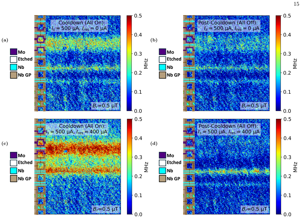
Superconductor digital electronics and quantum computing with superconducting qubits are promising next-generation computing technologies. When cooled down or operated in the presence of a nonzero background magnetic field $B_r$, superconducting thin films comprising the circuits can trap magnetic vortices that can degrade circuit or qubit performance. In this work, we report a practical solution for eliminating flux trapped during cooldown in ambient magnetic fields, $B_r\leq 60$ $\upmu$T, based on controlled local thermal gradients and moats, etched holes in the superconducting films of the circuit. Thermal gradients created by integrated on-chip resistive heaters move vortices towards the moats, where they become trapped away from circuitry regions and pinning sites. Using magnetic imaging and electrical circuit readout, we demonstrate that this approach is capable of removing magnetic flux trapped during field cooling and magnetic flux nucleated by circuit operation. If used in an environment with basic magnetic shielding, this solution is capable of suppressing all magnetic flux in a large-scale circuit, overcoming one of the long-standing challenges preventing high-performance scalable computing using superconductors.
Figures


Figures from the paper (9 more)


Reference graph
Works this paper leans on
-
[1]
Superconductor electronics,
T. Van Duzer, “Superconductor electronics,” Cryogenics 30, 980–995 (1990)
1990
-
[2]
Superconductor Electronics: Status and Outlook,
Alex I Braginski, “Superconductor Electronics: Status and Outlook,” Journal of Superconductivity and Novel Magnetism32, 23–44 (2019)
2019
-
[3]
Super- conductive electronics: A 25-year review [feature],
Rassul Bairamkulov and Giovanni De Micheli, “Super- conductive electronics: A 25-year review [feature],” IEEE Circuits and Systems Magazine24, 16–33 (2024)
2024
-
[4]
Co- herent control of macroscopic quantum states in a single- cooper-pair box,
Yasunobu Nakamura, Yu A Pashkin, and JS Tsai, “Co- herent control of macroscopic quantum states in a single- cooper-pair box,” nature398, 786–788 (1999)
1999
-
[5]
Charge-insensitive qubit design derived from the Cooper pair box,
Jens Koch, Terri M. Yu, Jay Gambetta, A. A. Houck, D. I. Schuster, J. Majer, Alexandre Blais, M. H. Devoret, S. M. Girvin, and R. J. Schoelkopf, “Charge-insensitive qubit design derived from the Cooper pair box,” Phys. Rev. A76, 042319 (2007)
2007
-
[6]
Coherent Josephson Qubit Suitable for Scalable Quantum Integrated Cir- cuits,
R. Barends, J. Kelly, A. Megrant, D. Sank, E. Jef- frey, Y. Chen, Y. Yin, B. Chiaro, J. Mutus, C. Neill, P. O’Malley, P. Roushan, J. Wenner, T. C. White, A. N. Cleland, and John M. Martinis, “Coherent Josephson Qubit Suitable for Scalable Quantum Integrated Cir- cuits,” Phys. Rev. Lett.111, 080502 (2013)
2013
-
[7]
A quantum engineer’s guide to superconducting qubits,
P. Krantz, M. Kjaergaard, F. Yan, T. P. Orlando, S. Gus- tavsson, and W. D. Oliver, “A quantum engineer’s guide to superconducting qubits,” Applied Physics Reviews6, 021318 (2019)
2019
-
[8]
Fluxonium: Single Cooper-Pair Circuit Free of Charge Offsets,
Vladimir E. Manucharyan, Jens Koch, Leonid I. Glaz- man, and Michel H. Devoret, “Fluxonium: Single Cooper-Pair Circuit Free of Charge Offsets,” Science 326, 113–116 (2009)
2009
Show all 70 references
-
[9]
Superconducting circuits for quantum information: An outlook,
M. H. Devoret and R. J. Schoelkopf, “Superconducting circuits for quantum information: An outlook,” Science 339, 1169–1174 (2013)
2013
-
[10]
AC-Biased Shift Registers as Fabrication Pro- cess Benchmark Circuits and Flux Trapping Diagnostic Tool,
Vasili K. Semenov, Yuri A. Polyakov, and Sergey K. Tolpygo, “AC-Biased Shift Registers as Fabrication Pro- cess Benchmark Circuits and Flux Trapping Diagnostic Tool,” IEEE Transactions on Applied Superconductivity 27, 1–9 (2017)
2017
-
[11]
Yield Evaluation of 10-kA/cm2 Nb Multi-Layer Fabrication Process Using Conventional Superconducting RAMs,
Shuichi Nagasawa, Tetsuro Satoh, Kenji Hinode, Yoshi- hiro Kitagawa, and Mutsuo Hidaka, “Yield Evaluation of 10-kA/cm2 Nb Multi-Layer Fabrication Process Using Conventional Superconducting RAMs,” IEEE Transac- tions on Applied Superconductivity17, 177–180 (2007)
2007
-
[12]
New ac-powered sfq digital circuits,
Vasili K. Semenov, Yuri A. Polyakov, and Sergey K. Tolpygo, “New ac-powered sfq digital circuits,” IEEE Transactions on Applied Superconductivity25, 1301507 (2015)
2015
-
[13]
Reproducible operating margins on a 72800-device digital supercon- ducting chip,
Quentin P Herr, Joshua Osborne, Micah J A Stoutimore, Harold Hearne, Ryan Selig, Jacob Vogel, Eileen Min, Vladimir V Talanov, and Anna Y Herr, “Reproducible operating margins on a 72800-device digital supercon- ducting chip,” Superconductor Science and Technology 28, 124003 (2015)
2015
-
[14]
Scalability of superconductor elec- tronics: Limitations imposed by ac clock and flux bias transformers,
Sergey K Tolpygo, “Scalability of superconductor elec- tronics: Limitations imposed by ac clock and flux bias transformers,” IEEE Transactions on Applied Supercon- ductivity33, 1–19 (2022)
2022
-
[15]
Fabrication pro- cess for superconducting digital circuits,
Mutsuo Hidaka and Shuichi Nagasawa, “Fabrication pro- cess for superconducting digital circuits,” IEICE Trans- actions on ElectronicsE104.C, 405–410 (2021)
2021
-
[16]
MANA: A Monolithic Adiabatic iNtegration Architec- ture Microprocessor Using 1.4-zJ/op Unshunted Super- conductor Josephson Junction Devices,
Christopher L. Ayala, Tomoyuki Tanaka, Ro Saito, Mai Nozoe, Naoki Takeuchi, and Nobuyuki Yoshikawa, “MANA: A Monolithic Adiabatic iNtegration Architec- ture Microprocessor Using 1.4-zJ/op Unshunted Super- conductor Josephson Junction Devices,” IEEE Journal of Solid-State Circu...
2021
-
[17]
Scaling up supercon- ducting quantum computers,
Anthony Megrant and Yu Chen, “Scaling up supercon- ducting quantum computers,” Nature Electronics8, 549– 551 (2025)
2025
-
[18]
Superconductor digital elec- tronics,
Konstantin K. Likharev, “Superconductor digital elec- tronics,” Physica C: Superconductivity and its Applica- tions482, 6–18 (2012)
2012
-
[19]
Superconductor digital electronics: Scalability and energy efficiency issues,
Sergey K Tolpygo, “Superconductor digital electronics: Scalability and energy efficiency issues,” Low Tempera- ture Physics42, 361–379 (2016)
2016
-
[20]
Supercon- ducting digital electronics,
S. Tahara, S. Yorozu, Y. Kameda, Y. Hashimoto, H. Nu- mata, T. Satoh, W. Hattori, and M. Hidaka, “Supercon- ducting digital electronics,” IEEE Transactions on Ap- plied Superconductivity11, 463–468 (2001)
2001
-
[21]
Progress Toward Superconductor Electronics Fabrica- tion Process With Planarized NbN and NbN/Nb Lay- ers,
Sergey K. Tolpygo, Justin L. Mallek, Vladimir Bolkhovsky, Ravi Rastogi, Evan B. Golden, Terence J. Weir, Leonard M. Johnson, and Mark A. Gouker, “Progress Toward Superconductor Electronics Fabrica- tion Process With Planarized NbN and NbN/Nb Lay- ers,” IEEE Transactions on App...
2023
-
[22]
Flexible NbTiN thin films for supercon- ducting electronics,
S.J. Rezinovsky Nieto, J.A. Hofer, M. Sirena, and N. Haberkorn, “Flexible NbTiN thin films for supercon- ducting electronics,” Physica C: Superconductivity and its Applications607, 1354241 (2023)
2023
-
[23]
NbTiN Based Two- Metal Level Semi-Damascene Interconnects, Josephson Junctions and Capacitors for Superconducting Digital Logic,
Ankit Pokhrel, Daniel P´ erez Lozano, Jean-Philippe Souli´ e, Diziana Vangoidsenhoven, Sujan K. Sarkar, Ra- 17 jendra K. Saroj, Yann Canvel, Vincent Renaud, Bart Kenens, Amey M. Walke, Jasper Bizindavyi, Sara Iraci, Seifallah Ibrahim, Blake Hodges, Trent Josephsen, Manu Perumk...
2024
-
[24]
Dielectric surface loss in superconducting resonators with flux-trapping holes,
B Chiaro, A Megrant, A Dunsworth, Z Chen, R Barends, B Campbell, Y Chen, A Fowler, IC Hoi, E Jeffrey,et al., “Dielectric surface loss in superconducting resonators with flux-trapping holes,” Superconductor Science and Technology29, 104006 (2016)
2016
-
[25]
Reducing microwave loss in super- conducting resonators due to trapped vortices,
Chunhua Song, Michael P DeFeo, Kang Yu, and Brit- ton LT Plourde, “Reducing microwave loss in super- conducting resonators due to trapped vortices,” Applied Physics Letters95(2009)
2009
-
[26]
Trapping a single vor- tex and reducing quasiparticles in a superconducting res- onator,
I Nsanzineza and BLT Plourde, “Trapping a single vor- tex and reducing quasiparticles in a superconducting res- onator,” Physical review letters113, 117002 (2014)
2014
-
[27]
Quantifying trapped magnetic vortex losses in niobium resonators at mk temperatures,
D Bafia, Bektur Abdisatarov, Roman Pilipenko, Yao Lu, G Eremeev, A Romanenko, and Anna Grassellino, “Quantifying trapped magnetic vortex losses in niobium resonators at mk temperatures,” Applied Physics Letters 127(2025)
2025
-
[28]
Extraction and simulation of the impact of flux trapping in moats on ac-biased shift registers,
Scott E. Meninger and Sergey K. Tolpygo, “Extraction and simulation of the impact of flux trapping in moats on ac-biased shift registers,” IEEE Transactions on Applied Superconductivity35, 1–6 (2025)
2025
-
[29]
Characterization of flux trapping in and fabrication of large-scale superconductor circuits us- ing AC-biased shift registers with 108500 Josephson junc- tions,
Evan B. Golden, Neel A. Parmar, Vasili K. Semenov, and Sergey K. Tolpygo, “Characterization of flux trapping in and fabrication of large-scale superconductor circuits us- ing AC-biased shift registers with 108500 Josephson junc- tions,” IEEE Transactions on Applied Superconduc...
2025
-
[30]
How moats protect superconductor films from flux trapping,
Vasili K Semenov and Mikhail M Khapaev, “How moats protect superconductor films from flux trapping,” IEEE Transactions on Applied Superconductivity26, 1300710 (2016)
2016
-
[31]
Moat-guarded Josephson SQUIDs,
S. Bermon and T. Gheewala, “Moat-guarded Josephson SQUIDs,” IEEE Transactions on Magnetics19, 1160– 1164 (1983)
1983
-
[32]
Magnetic imaging of moat-guarded supercon- ducting electronic circuits,
Mark Jeffery, T. Van Duzer, J. R. Kirtley, and M. B. Ketchen, “Magnetic imaging of moat-guarded supercon- ducting electronic circuits,” Applied Physics Letters67, 1769–1771 (1995)
1995
-
[33]
Experimental verification of moat design and flux trapping analysis,
Coenrad J Fourie and Kyle Jackman, “Experimental verification of moat design and flux trapping analysis,” IEEE Transactions on Applied Superconductivity31, 1– 7 (2021)
2021
-
[34]
Con- trolling magnetic flux penetration in low-T c supercon- ducting films and hybrids,
Fabiano Colauto, Maycon Motta, and WA Ortiz, “Con- trolling magnetic flux penetration in low-T c supercon- ducting films and hybrids,” Superconductor Science and Technology34, 013002 (2020)
2020
-
[35]
Mitigation of magnetic flux trapping in superconducting electronics using moats,
Rohan T. Kapur, Sergey K. Tolpygo, Alex Wynn, Pauli Kehayias, Adam A. Libson, Collin N. Muniz, Michael J. Gold, Justin L. Mallek, Danielle A. Braje, and Jen- nifer M. Schloss, “Mitigation of magnetic flux trapping in superconducting electronics using moats,” (2026), arXiv:2602...
2026 arXiv
-
[36]
Reducing vortex density in superconductors using the ‘ratchet effect’,
C-S Lee, Boldizsar Janko, Imre Derenyi, and A-L Barab´ asi, “Reducing vortex density in superconductors using the ‘ratchet effect’,” Nature400, 337–340 (1999)
1999
-
[37]
AC Defluxing of SQUIDs,
Andrei N. Matlashov, Vasili K. Semenov, and William H. Anderson, “AC Defluxing of SQUIDs,” IEEE Transac- tions on Applied Superconductivity27, 1–5 (2017)
2017
-
[38]
Manipulating vortex motion by thermal and lorentz force in high-temperature superconductors,
Zhi Wang, Lei Shan, YZ Zhang, J Yan, F Zhou, JW Xiong, WX Ti, and HH Wen, “Manipulating vortex motion by thermal and lorentz force in high-temperature superconductors,” Physical Review B—Condensed Mat- ter and Materials Physics72, 054509 (2005)
2005
-
[39]
Ibm releases first-ever 1,000- qubit quantum chip,
Davide Castelvecchiet al., “Ibm releases first-ever 1,000- qubit quantum chip,” Nature624, 238–238 (2023)
2023
-
[40]
D-Wave Quantum Inc.,Performance gains in the D- Wave Advantage2 system at the 4,400-qubit scale, Whitepaper 14-1083A-A (D-Wave Quantum Inc., 2025)
2025
-
[41]
Sweeping of trapped flux in superconducting films by a micro-heat-flushing method,
Q. Geng, H. Minami, K. Chihara, J. Yuyama, and E. Goto, “Sweeping of trapped flux in superconducting films by a micro-heat-flushing method,” Journal of Ap- plied Physics72, 2411–2417 (1992)
1992
-
[42]
Optical manipulation of single flux quanta,
Ivan S Veshchunov, William Magrini, SV Mironov, AG Godin, J-B Trebbia, Alexandre I Buzdin, Ph Tama- rat, and B Lounis, “Optical manipulation of single flux quanta,” Nature Communications7, 12801 (2016)
2016
-
[43]
Flux-trapping characterization for supercon- ducting electronics using a cryogenic widefield N-V dia- mond microscope,
Rohan T. Kapur, Pauli Kehayias, Sergey K. Tolpygo, Adam A. Libson, George Haldeman, Collin N. Muniz, Alex Wynn, Nathaniel J. O’Connor, Neel A. Parmar, Ryan Johnson, Andrew C. Maccabe, John Cummings, Justin L. Mallek, Danielle A. Braje, and Jennifer M. Schloss, “Flux-trapping c...
2026
-
[44]
Advanced fabrication processes for super- conducting very large-scale integrated circuits,
Sergey K. Tolpygo, Vladimir Bolkhovsky, T. J. Weir, Alex Wynn, D. E. Oates, L. M. Johnson, and M. A. Gouker, “Advanced fabrication processes for super- conducting very large-scale integrated circuits,” IEEE Transactions on Applied Superconductivity26, 1100110 (2016)
2016
-
[45]
Magnetic field effects in josephson junc- tions,
John R. Kirtley, “Magnetic field effects in josephson junc- tions,” inFundamentals and Frontiers of the Josephson Effect, edited by Francesco Tafuri (Springer International Publishing, Cham, 2019) pp. 209–233
2019
-
[46]
Michael Tinkham,Introduction to Superconductivity (Courier Corporation, 2004)
2004
-
[47]
Length-scale dependence of the superconductor- to-insulator quantum phase transition in one dimension,
Edmond Chow, Per Delsing, and David B. Havi- land, “Length-scale dependence of the superconductor- to-insulator quantum phase transition in one dimension,” Phys. Rev. Lett.81, 204–207 (1998)
1998
-
[48]
The current-phase relation in josephson junctions,
A. A. Golubov, M. Yu. Kupriyanov, and E. Il’ichev, “The current-phase relation in josephson junctions,” Rev. Mod. Phys.76, 411–469 (2004)
2004
-
[49]
Wafer-scale characterization of a superconductor inte- grated circuit fabrication process, using a cryogenic wafer prober,
Joshua T. West, Arthur Kurlej, Alex Wynn, Chad Rogers, Mark A. Gouker, and Sergey K. Tolpygo, “Wafer-scale characterization of a superconductor inte- grated circuit fabrication process, using a cryogenic wafer prober,” IEEE Transactions on Applied Superconductiv- ity32, 1–12 (2022)
2022
-
[50]
Flux pinning mechanisms in type ii superconductors,
D Dew-Hughes, “Flux pinning mechanisms in type ii superconductors,” Philosophical Magazine30, 293–305 (1974)
1974
-
[51]
Self-heating hotspots in superconducting thin-film mi- crobridges,
W. J. Skocpol, M. R. Beasley, and M. Tinkham, “Self-heating hotspots in superconducting thin-film mi- crobridges,” Journal of Applied Physics45, 4054–4066 (1974)
1974
-
[52]
Self-heating hotspots in superconduct- ing nanowires cooled by phonon black-body radiation,
Andrew Dane, Jason Allmaras, Di Zhu, Murat Onen, Marco Colangelo, Reza Baghdadi, Jean-Luc Tam- basco, Yukimi Morimoto, Ignacio Estay Forno, Ilya 18 Charaev,et al., “Self-heating hotspots in superconduct- ing nanowires cooled by phonon black-body radiation,” Nature Communicatio...
2022
-
[53]
Flux pinning by grain boundaries in niobium bicrys- tals,
A DasGupta, CC Koch, DM Kroeger, and YT Chou, “Flux pinning by grain boundaries in niobium bicrys- tals,” Philosophical Magazine B38, 367–380 (1978)
1978
-
[54]
Flux pinning characteristics in cylindrical niobium samples used for superconducting radio frequency cavity fabrication,
Asavari S Dhavale, Pashupati Dhakal, Anatolii A Polyan- skii, and Gianluigi Ciovati, “Flux pinning characteristics in cylindrical niobium samples used for superconducting radio frequency cavity fabrication,” Superconductor Sci- ence and Technology25, 065014 (2012)
2012
-
[55]
Hysteresis in super- conducting alloys—temperature and field dependence of dislocation pinning in niobium alloys,
W. A. Fietz and W. W. Webb, “Hysteresis in super- conducting alloys—temperature and field dependence of dislocation pinning in niobium alloys,” Phys. Rev.178, 657–667 (1969)
1969
-
[56]
Scanning vortex microscopy reveals thickness-dependent pinning nano-network in supercon- ducting niobium films,
Razmik A Hovhannisyan, Sergey Yu Grebenchuk, Se- men A Larionov, Andrey G Shishkin, Artem K Grebenko, Nadezhda E Kupchinskaya, Ekaterina A Dobrovolskaya, Olga V Skryabina, Alexey Yu Aladyshkin, Vyacheslav V Dremov,et al., “Scanning vortex microscopy reveals thickness-dependent...
2025
-
[57]
Flux pinning force in nb thin films with periodic vortex pinning arrays,
Lance Horng, Jong-Ching Wu, TC Wu, and SF Lee, “Flux pinning force in nb thin films with periodic vortex pinning arrays,” Journal of applied physics91, 8510–8512 (2002)
2002
-
[58]
Vortex dynam- ics in disordered niobium thin films,
Sameh M. Altanany, I. Zajcewa, T. Zajarniuk, A. Szewczyk, and Marta Z. Cieplak, “Vortex dynam- ics in disordered niobium thin films,” Phys. Rev. B109, 214504 (2024)
2024
-
[59]
Controlled manipulation of individual vortices in a superconductor,
Eric WJ Straver, Jennifer E Hoffman, Ophir M Auslaen- der, Daniel Rugar, and Kathryn A Moler, “Controlled manipulation of individual vortices in a superconductor,” Applied Physics Letters93(2008)
2008
-
[60]
Vortex pinning force in a super- conducting niobium strip,
George S. Park, Charles E. Cunningham, Blas Cabrera, and Martin E. Huber, “Vortex pinning force in a super- conducting niobium strip,” Phys. Rev. Lett.68, 1920– 1922 (1992)
1920
-
[61]
On the theory of super- conductivity,
VL Ginzburg and LD Landau, “On the theory of super- conductivity,” Zh. Eksp. Teor. Fiz20, 1064 (1950)
1950
-
[62]
Critical current for super- conducting films,
Vitalii Lazarevich Ginzburg, “Critical current for super- conducting films,” inDoklady Akademii Nauk, Vol. 118 (Russian Academy of Sciences, 1958) pp. 464–467
1958
-
[63]
Critical fields and currents in supercon- ductors,
John Bardeen, “Critical fields and currents in supercon- ductors,” Rev. Mod. Phys.34, 667–681 (1962)
1962
-
[64]
Interaction between a cavity and a vortex in a superconductor of the second kind,
GS Mkrtchyan and VV Shmidt, “Interaction between a cavity and a vortex in a superconductor of the second kind,” Soviet Physics JETP34, 195–197 (1972)
1972
-
[65]
Thermal conductivity and specific heat of noncrystalline solids,
R. C. Zeller and R. O. Pohl, “Thermal conductivity and specific heat of noncrystalline solids,” Phys. Rev. B4, 2029–2041 (1971)
-
[66]
Nanoscale ther- mal transport,
David G Cahill, Wayne K Ford, Kenneth E Goodson, Gerald D Mahan, Arun Majumdar, Humphrey J Maris, Roberto Merlin, and Simon R Phillpot, “Nanoscale ther- mal transport,” Journal of applied physics93, 793–818 (2003)
2003
-
[67]
Thermal boundary resis- tance,
E. T. Swartz and R. O. Pohl, “Thermal boundary resis- tance,” Rev. Mod. Phys.61, 605–668 (1989)
1989
-
[68]
Dendritic flux avalanches and nonlocal electrodynamics in thin superconducting films,
Igor S Aranson, Alex Gurevich, Marco S Welling, Rinke J Wijngaarden, Vitalii K Vlasko-Vlasov, Valerii M Vi- nokur, and Ulrich Welp, “Dendritic flux avalanches and nonlocal electrodynamics in thin superconducting films,” Physical review letters94, 037002 (2005)
2005
-
[69]
Boundary layer model for vor- tex fingers in type-ii superconductors,
Chiara Baggio, Raymond E Goldstein, Adriana I Pesci, and Wim van Saarloos, “Boundary layer model for vor- tex fingers in type-ii superconductors,” Physical Review B—Condensed Matter and Materials Physics72, 060503 (2005)
2005
-
[70]
Thermally controlled flux avalanche dynamics in the bulk superconductor nbti,
I Abaloszewa, VV Chabanenko, and A Abaloszew, “Thermally controlled flux avalanche dynamics in the bulk superconductor nbti,” Physical Review B113, 104511 (2026)
2026
Reviewed June 29, 2026 · model on record in the stance chip above.
Discussion (0). Continue with ORCID to comment.