REVIEW 2 major objections 4 minor 35 references
A narrow Si well with a pure-Ge cap and dilute Ge spike can push valley splitting to 1–5 meV with low disorder spread.
Reviewed by Pith at T0; open to challenge. T0 means a machine referee read the full paper against a public rubric. the ladder, T0–T4 →
T0 review · grok-4.5
2026-07-13 01:26 UTC pith:ETFOEWCG
load-bearing objection Clean, falsifiable heterostructure recipe that could remove valley splitting as a scaling bottleneck if 1–2 ML interfaces can be grown. the 2 major comments →
Silicon-Germanium Heterostructures with Enhanced Valley Splitting for Spin Qubits
The pith
A machine-rendered reading of the paper's core claim, the machinery that carries it, and where it could break.
Core claim
Combining a narrow (2.5–3 nm) silicon quantum well, a one-monolayer pure-Ge cap, and a dilute Ge spike at the well center yields valley splittings of order 1–5 meV with a narrow statistical spread across alloy realizations, provided the cap and spike interfaces remain 1–2 monolayers wide.
What carries the argument
2k0 theory (a single-band effective-mass Hamiltonian equivalent to a two-band tight-binding model) that evaluates the Fourier component of the alloy potential at the inter-valley wave-vector 2k0; the pure-Ge cap and central Ge spike are engineered to maximize that component while keeping Ge content low.
Load-bearing premise
That a pure-Ge cap and dilute Ge spike can actually be grown with interface widths of only one or two atomic layers while preserving the wave-function overlap that produces the large valley splitting.
What would settle it
Grow the proposed stack (2.5–3 nm well, 1 ML Ge cap, ~4 % central Ge spike) and measure valley splitting on many devices; if the median remains below ~1 meV or the spread is large, the predicted ceiling has not been reached.
If this is right
- Valley splitting would cease to be an existential yield limiter for large Si/SiGe quantum processors.
- Only one heterostructure improvement beyond present growth—either a 2.5 nm well or 1–2 ML-sharp cap/spike interfaces—is required to reach Ev ≳ 1 meV.
- The dilute spike and pure-Ge cap are thermodynamically favored to stay sharp, reducing the risk of interdiffusion during growth.
- Standard gate layouts already demonstrated on 3 nm wells remain usable, so device redesign is minimal.
Where Pith is reading between the lines
- If the 1–2 ML interface target is met, the same design could also suppress valley-related leakage during long-distance spin shuttling.
- The additive boost from even a few-percent Ge spike suggests that further reduction of Ge content (to minimize spin–orbit) may still be viable if interfaces stay sharp.
- The same Fourier-weight principle could be applied to other group-IV heterostructures where valley degeneracy is a problem.
Editorial analysis
A structured set of objections, weighed in public.
Referee Report
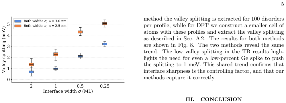
Summary. The manuscript proposes a Si/SiGe heterostructure that combines a narrow (2.5–3.0 nm) quantum well, a single-monolayer pure-Ge cap, and a dilute (~4 %) Ge spike at the well center. Using a 2k0/tight-binding model that incorporates atomistic alloy disorder (100 realizations per configuration) together with corroborating DFT calculations on selected Ge profiles, the authors show that this design can produce valley splittings of 1–5 meV with a comparatively tight distribution when the critical interfaces remain 1–2 ML wide. Parameter sweeps over well width, cap thickness, spike fraction, and interface widths establish an idealized ceiling and then quantify how that ceiling erodes under realistic interdiffusion. The central claim is that, if the required interface sharpness is achieved, valley splitting ceases to be an existential obstacle for large-scale Si/SiGe spin-qubit processors.
Significance. If the predicted valley-splitting distributions can be realized experimentally, the work would remove one of the principal materials bottlenecks for scaling Si/SiGe spin qubits. The combination of three design elements (narrow well + pure-Ge cap + dilute spike) is unorthodox relative to prior proposals, and the transparent disorder statistics (box-and-whisker plots over 100 alloy realizations) plus dual TB/DFT trend agreement constitute a clear, falsifiable prediction. The thermodynamic arguments offered for why a pure-Ge cap and dilute spike should be sharper than conventional 30 % SiGe interfaces further strengthen the experimental roadmap. These strengths make the manuscript a valuable contribution to the device-physics literature even if growth challenges remain.
major comments (2)
- Sec. II B and Fig. 7: the claim that Ev ≳ 1 meV with a tight distribution is load-bearing on interface widths σcap, σspike of only 1–2 ML (together with Ww = 2.5–3.0 nm). The paper itself shows that broader interfaces collapse the splitting below 1 meV. While thermodynamic arguments for sharpness are given, no quantitative growth model or existing experimental demonstration of the combined profile is supplied. The manuscript should either (i) cite or present growth data that already approach these widths for pure-Ge caps / dilute spikes on thin wells, or (ii) reframe the central claim more explicitly as a conditional prediction whose experimental verification is the next required step.
- Appendix A and the strain discussion in the methods: strain effects beyond fixing the valley minima at ±k0 = 0.82 × 2π/a0 are neglected. For a pure-Ge cap and a Ge spike inside a 2.5–3 nm well the local strain landscape is non-uniform; even modest strain-induced shifts of the envelope or of the 2k0 Fourier component could alter the predicted ceiling. A short estimate (or a statement that full atomistic strain relaxation was checked for the DFT cells and found negligible) would strengthen confidence that the approximation does not undercut the 1–5 meV claim.
minor comments (4)
- Fig. 5 caption and surrounding text: the DFT points are described as “two effective disorder realizations,” but the precise construction of those cells (SQS size, lateral periodicity) is only partially specified in Appendix A2; a one-sentence clarification would help readers assess the comparison.
- Table I lists σi = 2.0 ML as a baseline, yet the idealized-interface sweeps of Sec. II A set interfaces to atomically sharp; the dual use of σi is slightly confusing and could be clarified in the table caption.
- Several arXiv preprints are cited as “recently reported” (e.g., Refs. [4], [8], [18], [20], [33]); if any have since been published, the journal versions should be substituted before final acceptance.
- Typographical inconsistencies appear in a few places (e.g., “The approachrestsonanunorthodox”, missing spaces after periods in the abstract and introduction). A careful copy-edit pass is needed.
Circularity Check
No significant circularity: valley-splitting predictions are forward simulations of an established Hamiltonian over design parameters, not fits or self-definitional reductions.
full rationale
The paper's central claim is that a specific Si/SiGe heterostructure (narrow well Ww = 2.5-3.0 nm, 1 ML pure-Ge cap, dilute fGe ~ 0.04 spike) produces Ev of 1-5 meV with tight disorder distributions when interfaces are 1-2 ML wide. This is obtained by solving a single-band effective-mass / 2k0 Hamiltonian (Appendix A, equivalent to prior TB models of Refs. [5,24]) whose parameters (mxy, mz, k0 = 0.82 * 2pi/a0, band-offset formula of Ref. [26]) are taken from the literature and held fixed. Design parameters (NML, Ww, fGe, sigma_cap, sigma_spike) are swept; 100 independent alloy realizations are generated for each point; Ev is extracted as the energy difference of the lowest non-orbital states. No parameter is fitted to a target splitting, no uniqueness theorem is imported from the authors, and no equation reduces Ev to a quantity defined by the result itself. DFT comparisons (Figs. 5, 8) use independent SQS supercells and serve only as trend corroboration. Self-citations are to methods or prior heterostructure ideas, not to the numerical outcome. The derivation is therefore self-contained and non-circular; growth attainability of the assumed interface widths is an experimental risk, not a circularity.
Axiom & Free-Parameter Ledger
free parameters (5)
- well width Ww =
2.5-3.0 nm
- Ge spike fraction fGe =
0.04
- pure-Ge cap thickness NML =
1 ML
- interface widths σcap, σspike =
1-2 ML
- vertical field Fz and orbital energies ħωx,y =
5 MV/m, 2.5 meV
axioms (5)
- domain assumption Valley splitting is set by the Fourier component of the confining potential at wave-vector 2k0 that couples the ±z valleys.
- domain assumption Alloy disorder can be modeled by independent Bernoulli occupation of diamond-lattice sites with position-dependent Ge probability χGe(z), mapped onto a finer simulation grid by linear interpolation.
- domain assumption Conduction-band offset follows the strained-on-SiGe virtual-crystal expression of Schäffler (1997) linearly rescaled by local Si content.
- ad hoc to paper Strain effects beyond fixing the valley minima at ±k0 = ±0.82×2π/a0 can be ignored.
- domain assumption A pure-Ge cap and dilute Ge spike are thermodynamically sharper than conventional 30 % SiGe interfaces because Ge-Ge bonding energy is suppressed.
read the original abstract
Achieving valley splittings well in excess of the thermal energy of electrons and avoiding valley excitations is essential for the consistent initialization, operation and readout of gate-defined Si spin qubits. In this work, we present a device-level optimization strategy for pushing valley splittings to between 1 and 5 meV, well beyond values reported in nearly all previous theoretical studies. Using device-scale simulations that incorporate atomistic alloy disorder through a 1D tight-binding theory, we demonstrate that our proposed approach yields large valley splittings with a tight distribution across disorder realizations, a key requirement for reproducible qubit performance at scale. The approach rests on an unorthodox Si/SiGe heterostructure design combining a narrow quantum well, a small Ge spike, and a pure-Ge cap. We corroborate these predictions with targeted atomistic density functional theory calculations. These results offer a clear path forward for scalable Si/SiGe spin qubit devices and, if realized experimentally, effectively eliminate valley splitting as an existential problem for large scale SiGe-based quantum processors.
Figures




Reference graph
Works this paper leans on
-
[1]
F. A. Zwanenburg, A. S. Dzurak, A. Morello, M. Y. Sim- mons, L. C. L. Hollenberg, G. Klimeck, S. Rogge, S. N. Coppersmith, and M. A. Eriksson, Rev. Mod. Phys.85, 961 (2013)
2013
-
[2]
Burkard, T
G. Burkard, T. D. Ladd, A. Pan, J. M. Nichol, and J. R. Petta, Rev. Mod. Phys.95, 025003 (2023)
2023
-
[3]
Neyens, O
S. Neyens, O. K. Zietz, T. F. Watson, F. Luthi, A. Neth- wewala, H. C. George, E. Henry, M. Islam, A. J. Wag- ner, F. Borjans, E. J. Connors, J. Corrigan, M. J. Curry, D. Keith, R. Kotlyar, L. F. Lampert, M. T. Mądzik, K. Millard, F. A. Mohiyaddin, S. Pellerano, R. Pil- larisetty, M. Ramsey, R. Savytskyy, S. Schaal, G. Zheng, J. Ziegler, N. C. Bishop, S. ...
2024
-
[4]
Optimization of Si/SiGe Heterostruc- tures for Large and Robust Valley Splitting in Silicon Qubits,
A. Thayil, L. Ermoneit, L. R. Schreiber, T. Koprucki, and M. Kantner, “Optimization of Si/SiGe Heterostruc- tures for Large and Robust Valley Splitting in Silicon Qubits,” (2025), arXiv:2512.18064 [cond-mat.mes-hall]
arXiv 2025
-
[5]
M. P. Losert, M. A. Eriksson, R. Joynt, R. Rahman, G. Scappucci, S. N. Coppersmith, and M. Friesen, Phys- ical Review B108, 125405 (2023)
2023
-
[6]
McJunkin, B
T. McJunkin, B. Harpt, Y. Feng, M. P. Losert, R. Rah- man, J. P. Dodson, M. A. Wolfe, D. E. Savage, M. G. Lagally, S. N. Coppersmith, M. Friesen, R. Joynt, and M.A.Eriksson,NatureCommunications13,7777(2022)
2022
-
[7]
B. D. Woods, H. Soomro, E. S. Joseph, C. C. D. Frink, R. Joynt, M. A. Eriksson, and M. Friesen, npj Quantum Information10, 54 (2024)
2024
-
[8]
Increasing valley splitting in Si/SiGe by practically achievable heterostructure profiles,
L. Cvitkovich, P. Stano, D. Bougeard, Y.-M. Niquet, and D. Loss, “Increasing valley splitting in Si/SiGe by practically achievable heterostructure profiles,” (2026), arXiv:2603.19769 [cond-mat.mes-hall]
arXiv 2026
-
[9]
Paquelet Wuetz, M
B. Paquelet Wuetz, M. P. Losert, S. Koelling, L. E. A. Stehouwer, A.-M. J. Zwerver, S. G. J. Philips, M. T. Mądzik, X. Xue, G. Zheng, M. Lodari, S. V. Amitonov, N. Samkharadze, A. Sammak, L. Vandersypen, R. Rah- man, S. N. Coppersmith, O. Moutanabbir, M. Friesen, and G. Scappucci, Nature Communications13, 7730 (2022)
2022
-
[10]
S. F. Neyens, R.H. Foote, B. Thorgrimsson, T. J. Knapp, T. McJunkin, L. M. K. Vandersypen, P. Amin, N. K. Thomas, J. S. Clarke, D. E. Savage, M. G. Lagally, M. Friesen, S. N. Coppersmith, and M. A. Eriksson, Applied Physics Letters112, 243107 (2018)
2018
-
[11]
Zhang, J.-W
L. Zhang, J.-W. Luo, A. Saraiva, B. Koiller, and A. Zunger, Nature Communications4, 2396 (2013)
2013
-
[12]
A. A. Williams, J. M. C. Thornton, J. E. Macdonald, R. G. van Silfhout, J. F. van der Veen, M. S. Finney, A. D. Johnson, and C. Norris, Physical Review B43, 5001 (1991)
1991
-
[13]
F. Liu, F. Wu, and M. G. Lagally, Chemical Reviews 97, 1045 (1997)
1997
-
[14]
L. E. A. Stehouwer, M. P. Losert, M. Rigot, D. Degli Es- posti, S. Martí-Sánchez, M. Rimbach-Russ, J. Arbiol, M. Friesen, and G. Scappucci, Nano Letters25, 12892 (2025)
2025
-
[15]
B. D. Woods, M. A. Eriksson, R. Joynt, and M. Friesen, Physical Review B107, 035418 (2023)
2023
-
[16]
E. H. Chen, K. Raach, A. Pan, A. A. Kiselev, E. Acuna, J. Z. Blumoff, T. Brecht, M. D. Choi, W. Ha, D. R. Hul- bert, M. P. Jura, T. E. Keating, R. Noah, B. Sun, B. J. Thomas, M. G. Borselli, C. Jackson, M. T. Rakher, and R. S. Ross, Physical Review Applied15, 044033 (2021)
2021
-
[17]
Acuna, J
E. Acuna, J. D. Broz, K. Shyamsundar, A. B. Mei, C. P. Feeney, V. Smetanka, T. Davis, K. Lee, M. D. Choi, B. Boyd, J. Suh, W. Ha, C. Jennings, A. S. Pan, D. S. Sanchez, M. D. Reed, and J. R. Petta, Physical Review Applied22, 044057 (2024)
2024
-
[18]
A digi- tally controlled silicon quantum processing unit,
M. of the HRL Quantum Team, Collaborators, M. Abra- ham, E. Acuna, T. S. Adams, M. Akmal, M. R. Alfaro, I. Alvarado, J. Amontree, C. Andrews, R. W. Andrews, M. Antcliffe, A. R. Aséncio, R. M. A. Batres, C. D. Baringer, D. W. Barnes, K. M. Beech, R. G. Blakey, Z. T. Bloom, A. J. Bluestone, J. Z. Blumoff,et al., “A digi- tally controlled silicon quantum pro...
Pith/arXiv arXiv 2026
-
[19]
E. J. Connors, J. Nelson, H. Qiao, L. F. Edge, and J. M. Nichol, Phys. Rev. B100, 165305 (2019)
2019
-
[20]
Exact Multi-Valley Envelope Function Theory of Valley Splitting in Si/SiGe Nanostructures,
L. Ermoneit, A. Thayil, T. Koprucki, and M. Kant- ner, “Exact Multi-Valley Envelope Function Theory of Valley Splitting in Si/SiGe Nanostructures,” (2026), arXiv:2602.14787 [cond-mat.mes-hall]
Pith/arXiv arXiv 2026
-
[21]
M. P. R. Losert, U. Güngördü, S. N. Coppersmith, M. Friesen, and C. Tahan, Physical Review B113, 235301 (2026)
2026
-
[22]
Young, M
S. Young, M. Brickson, J. R. Petta, and N. T. Jacobson, Physical Review Applied24, 064042 (2025)
2025
-
[23]
Cvitkovich, T
L. Cvitkovich, T. Salamone, C. Wilhelmer, B. Martinez, T. Grasser, and Y.-M. Niquet, Physical Review B113, 035307 (2026)
2026
-
[24]
T. B. Boykin, G. Klimeck, M. A. Eriksson, M. Friesen, S. N. Coppersmith, P. von Allmen, F. Oyafuso, and S. Lee, Applied Physics Letters84, 115 (2004)
2004
-
[25]
C. R. Anderson, Journal of Computational Physics229, 7477 (2010)
2010
-
[26]
Schäffler, Semiconductor Science and Technology12, 1515 (1997)
F. Schäffler, Semiconductor Science and Technology12, 1515 (1997)
1997
-
[27]
Kresse and J
G. Kresse and J. Hafner, Phys. Rev. B47, 558 (1993)
1993
-
[28]
Kresse and J
G. Kresse and J. Furthmuller, Comput. Mater. Sci.6, 15 (1996)
1996
-
[29]
J. P. Perdew, A. Ruzsinszky, G. I. Csonka, O. A. Vydrov, G.E.Scuseria, L.A.Constantin, X.Zhou, andK.Burke, Phys. Rev. Lett.100, 136406 (2008)
2008
-
[30]
Zunger, S.-H
A. Zunger, S.-H. Wei, L. G. Ferreira, and J. E. Bernard, Phys. Rev. Lett.65, 353 (1990)
1990
-
[31]
A. v. d. Walle, M. Asta, and G. Ceder, Calphad26, 539 (2002)
2002
-
[32]
J. P. Dismukes, Ekstrom, and R. J. Paff, J. Phys. Chem. 68, 3021 (1964)
1964
-
[33]
I. Rahlff, C. Richter, M. Schmidbauer, M. Oezkent, T. Remmele, M. Hanke, L. R. Schreiber, D. Dütz, S. Umezawa, M. Albrecht, Y.-M. Niquet, T. Salamone, B. M. Diaz, T. Schroeder, J. Martin, and K.-P. Grad- wohl, “Sharp periodic Ge concentration modulations be- yond the conduction band valley wavevectork0 in nuclear spin-free Si quantum wells,” (2026), arXiv...
Pith/arXiv arXiv 2026
-
[34]
Single-particle Hamiltonian The single-particle Hamiltonian takes the form Hsp(r) =H kin(r) +V(r),(A1) whereH kin is the effective-mass kinetic operator and V(r)is the position-dependent potential. The kinetic operator is calculated in momentum space, wherethetwovalleysappearasparabolicminimaatk z = ±k0 withk 0 = 0.82×2π/a 0 anda 0 the silicon lattice con...
-
[35]
DFT modeling DFT calculations are carried out using the Vienna Ab-initio Simulation Package (VASP) [27, 28]. We use the PBEsol [29] exchange-correlation energy functional for the structural optimizations since this functional is known to be able to reproduce accurately the structural parameters for solids. Periodic SiGe/Si/SiGe superlat- tice structures, ...
discussion (0)
Sign in with ORCID, Apple, or X to comment. Anyone can read and Pith papers without signing in.