REVIEW 3 major objections 5 minor 1 cited by
Characterising Quantum Devices at Scale with Custom Cryo-CMOS
T0 review · 3 major / 5 minor · reviewed 2026-08-14 · deepseek-v4-flash
Pith's one-line read A custom cryo-CMOS multiplexer lets multiple quantum devices share one dilution-refrigerator cool-down without degrading device performance.
desk verdict A genuinely useful cryo-CMOS multiplexer demonstration for batch quantum device characterization, but the 'no degradation' claim needs a direct wired baseline and the field-dependent series resistance needs to be quantified or subtracted. read the letter →
The pith
A machine-rendered reading of the paper's core claim, the machinery that carries it, and where it could break.
The reading
What carries the argument
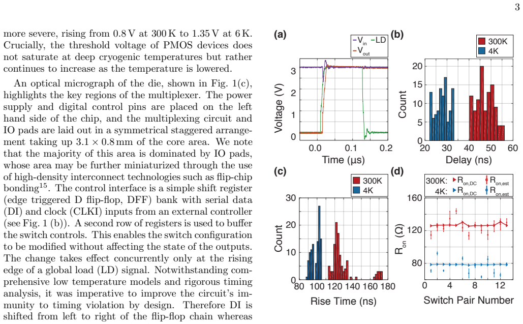
The central object is a cryo-CMOS multiplexer chip: 16 1:5 analog switches per die, each a transmission gate of parallel NMOS and PMOS transistors allowing rail-to-rail voltage swing, together with an edge-triggered shift-register control bank and buffered clock and data lines for daisy chaining without extra control wires. The transmission-gate topology is what lets a single chip route both positive and negative bias voltages and pass transport currents with on-state resistance below 200 Ω at 4 K. The shift-register plus load-signal design lets the switch configuration be updated without disturbing the outputs and spreads clock current draw, a pragmatic fix for the long cable runs and loose timing of cryogenic wiring.
What would settle it
On a single cool-down, measure Coulomb-blockade peak width or tunnel-current noise of a quantum dot through the multiplexer and then through a bypass line that connects the same device directly to the same electronics; if the extracted electron temperature or noise floor rises when the multiplexer is in the signal path, the claim of transparency fails.
Extended reading notes
Core claim
With a custom cryo-CMOS multiplexer built from 16 transmission-gate 1:5 switches per die, the authors characterize multiple quantum devices in a single dilution-refrigerator cool-down using standard wiring. They tune a GaAs double quantum dot through the multiplexer into the few-electron regime and observe the characteristic honeycomb charge-stability pattern, and they map Hall mobility across an InAs wafer, measuring nine devices over two cool-downs with no degradation compared with devices wired directly. The multiplexer is controlled by a shift-register bank, can be daisy-chained without adding control lines, and is operated over a supply range that allows negative gate biases.
Load-bearing premise
The load-bearing premise is that placing the cryo-CMOS multiplexer in series with the device adds negligible electrical noise and heat at millikelvin temperatures, so the device behaves as it would with direct wiring.
Editorial extensions
If this is right
- Batch characterization means wafer-scale mobility maps can be produced in one or two cool-downs, giving fast feedback between epitaxial growth and device performance.
- The same wiring configuration and control lines can drive many more devices by daisy chaining multiplexer chips, because the control-line count does not grow with switch count.
- Because the multiplexer introduces no measurable steady-state thermal load, the cryostat base temperature is preserved, so devices remain in the same physical regime as direct-wired devices.
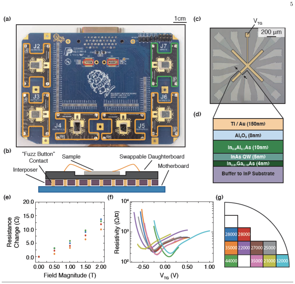
- The inline resistance of about 6 Ω/T in a perpendicular magnetic field must be accounted for in transport data, but it is small and linear over the ±2 T range studied.
Reading between the lines
- The same platform could extend beyond GaAs and InAs to silicon spin qubits or superconducting circuits, since the multiplexer is agnostic to device technology as long as voltage and current ranges fit the transmission gates.
- A direct wired-only control measurement on the same cool-down would quantify the added noise floor and electron temperature, turning the transparency claim from inferred to measured; the bypass connection already included in the test package makes this test straightforward.
- Daisy chaining to larger switch counts will eventually trade switching speed against control-line count, so the architecture's practical limit is not device count but how often the configuration needs to change.
Signed reviews
Editorial analysis
A structured set of objections, weighed in public.
Referee Report
Summary. The paper reports a custom cryo-CMOS multiplexer (MUX) chip and a modular packaging platform intended to allow batch characterization of quantum devices in a single dilution-refrigerator cool-down. The MUX uses transmission-gate switches, a shift-register control interface with daisy-chaining capability, and is benchmarked at 300 K and 4 K in terms of switching delay, rise time, and on-resistance. The authors demonstrate two applications: tuning a GaAs double quantum dot to the few-electron regime with gates and contacts routed through the MUX, and measuring Hall mobility across an InAs heterostructure wafer with nine devices in two cool-downs. They report a field-dependent inline resistance of about 6 Ω/T in the range −2 T to 2 T and state that no degradation in device performance is seen relative to direct wiring. The central claim is that the MUX is transparent enough to enable multiplexed low-temperature device characterization without compromising device performance.
Significance. If the central transparency claim is established, this is a useful engineering contribution to the quantum-device characterization pipeline. The use of a commercial CMOS foundry for the multiplexer, the modular daughter-board packaging, the daisy-chaining scheme, and the extension to wafer-scale mobility mapping are practical advances that could save substantial refrigerator time. The paper also provides concrete switch metrics (on-resistance below 200 Ω, 4 K delay and rise-time histograms) and honestly acknowledges a competing preprint. However, the significance of the platform rests on the multiplexer being electrically and thermally invisible to the device under test; the current evidence is qualitative. The quantum-dot honeycomb demonstrates functionality, and the base-temperature statement shows no gross thermal load, but the absence of a quantitative direct-wiring baseline means the central 'no degradation' claim is not yet supported to the standard the paper itself sets.
major comments (3)
- [Section III.B and Fig. 4(a), 4(f), 4(g)] The central claim that the MUX causes 'no degradation in device performance' compared to direct wiring is not supported by quantitative comparison data. The green daughter-board in Fig. 4(a) explicitly provides a bypass path that routes the fridge wiring around the MUX, yet no measurements taken through this bypass are reported. I request a same-device or identical-device comparison of Hall resistivity, extracted mobility, and measurement noise with the MUX in-line versus bypassed, including uncertainties. This is load-bearing because the entire platform's value is that the MUX is transparent.
- [Section III.B and Fig. 4(e)] Figure 4(e) shows an additional inline resistance of approximately 6 Ω/T over the −2 T to 2 T range. The manuscript does not state whether this field-dependent series resistance was subtracted from the Hall resistivity data used to extract mobility, nor how any residual uncertainty propagates into the mobility values in Fig. 4(g). If this resistance is not fully characterized and accounted for, the extracted mobility will be biased by a field-dependent offset, and the transparency claim at high magnetic field is not established. Please provide the correction procedure and its effect on the reported mobility map.
- [Section III.A] The statement that 'the additional heat or noise generated by the MUX chip is negligible' is supported only by the observation that the cryostat base temperature is unaffected and by the visibility of a honeycomb charge stability diagram. Base temperature is a weak proxy for the electrical noise the MUX can inject into gate lines or transport lines. A quantitative measure such as the electron temperature extracted from Coulomb-peak widths, or a noise comparison between the MUX path and a direct-wired path, is needed to substantiate the claim that the MUX is electrically transparent for quantum-dot operation.
minor comments (5)
- [Section II, Eq. (1)] Equation (1) as typeset appears dimensionally inconsistent: the on-resistance should scale as L/(µCox W (VGS−Vth)), not W/(µCox L (VGS−Vth)) as printed. Please correct the equation and the surrounding discussion.
- [Section III.B, Fig. 4(g)] The mobility map in Fig. 4(g) has no color scale, error bars, or caption indicating the uncertainty in each mobility value; adding these would strengthen the batch-characterization claim.
- [Abstract and Section III.B] The term 'hot-swappable' is used to describe the daughter-board platform, but the text says samples are interchanged between cool-downs. Please clarify whether the intent is interchange at room temperature or at cryogenic temperatures to avoid overstating the capability.
- [Fig. 1(c) caption] The label 'I2O2,5' in the die photo is not defined in the text or caption; a brief description would help the reader interpret the chip layout.
- [Final note, Ref. [22]] The closing note about a similar preprint from another group is useful, but consider integrating that comparison into the introduction or discussion so that the distinction from commercial off-the-shelf CMOS multiplexing is established in the main body.
Circularity Check
No significant circularity: the paper is an experimental benchmarking report, and no fitted parameter or self-citation is presented as a prediction that reduces to its own inputs.
full rationale
The paper's load-bearing content is direct experimental work: a custom cryo-CMOS multiplexer is described, and its performance is assessed through on-state resistance measurements, few-electron double-quantum-dot stability diagrams, and Hall mobility mapping. The on-resistance model in Eqs. (1)-(3) is the standard ohmic-region transistor expression; the cryogenic ratios gamma_n and gamma_p use independently obtained mobility and threshold-voltage shifts, and they are not fitted to the later device characterization data. The reported agreement between Ron,est (derived from rise-time and cable capacitance) and Ron,DC (measured with lock-in techniques) is an empirical cross-check of two independent measurement channels, not a constructed identity. The central 'no degradation' claim for the MUX is supported qualitatively by the quantum-dot honeycomb, the statement that the cryostat base temperature is unaffected, and a sentence asserting no degradation in Hall measurements; the paper does not show a quantitative direct-wired baseline despite having a bypass daughter-board. That is an evidentiary gap or an unsupported assertion, not circularity: no output quantity is defined in terms of the transparency claim. The self-citations (refs. 3, 17, 21) provide background on cryogenic control, charging-energy scale, and modular interconnects; even where the authors overlap with the present work, these citations are not used to define the measured quantities, to forbid alternative interpretations, or to supply a uniqueness theorem. The observed field-dependent inline resistance of 6 ohm/T is reported as a measured effect rather than an input from which the Hall data are derived. No fitted parameter is renamed as a prediction, and no equation reduces to its own input by construction. The appropriate finding is therefore no significant circularity.
Assumptions & free parameters
assumptions (3)
- domain assumption Transmission gate switches operate in the ohmic region in steady state with VDS << 10 mV, so the on-resistance formula (Eq. 1) is valid.
- domain assumption Standard Hall effect and mobility extraction formulas apply to the InAs quantum well at milli-Kelvin temperatures and magnetic fields up to ±2 T.
- domain assumption The cryo-CMOS MUX introduces negligible heat and noise at milli-Kelvin, so device performance is unperturbed.
Cite this review
Pith. "Pith review of Characterising Quantum Devices at Scale with Custom Cryo-CMOS." pith.science (2026). https://pith.science/paper/76MUBN6H
@misc{pith2026190807685,
  author       = {Pith},
  title        = {Pith review of: Characterising Quantum Devices at Scale with Custom Cryo-CMOS},
  year         = {2026},
  howpublished = {\url{https://pith.science/paper/76MUBN6H}},
  note         = {Machine review of arXiv:1908.07685}
}
read the original abstract
We make use of a custom-designed cryo-CMOS multiplexer (MUX) to enable multiple quantum devices to be characterized in a single cool-down of a dilution refrigerator. Combined with a packaging approach that integrates cryo-CMOS chips and a hot-swappable, parallel device test platform, we describe how this setup takes a standard wiring configuration as input and expands the capability for batch-characterization of quantum devices at milli-Kelvin temperatures and high magnetic fields. The architecture of the cryo-CMOS multiplexer is discussed and performance benchmarked using few-electron quantum dots and Hall mobility-mapping measurements.
Figures


Figures from the paper (1 more)
Forward citations
Cited by 1 Pith paper
-
Repairing the Surface of InAs-based Topological Heterostructures
An Ar-H plasma applied before aluminum-oxide growth raises peak mobility in shallow InAs quantum wells to 45,300 cm2/Vs and lowers sample-to-sample variance compared with untreated or TMA-treated samples.
Reference graph
Works this paper leans on
-
[1]
3D integration and packaging for solid-state qubits
author author D. Rosenberg , author S. Weber , author D. Conway , author D. Yost , author J. Mallek , author G. Calusine , author R. Das , author D. Kim , author M. Schwartz , author W. Woods , author J. L. \ Yoder , and\ author W. D. \ Oliver ,\ title title 3D integration and packaging for solid-state qubits ,\ @noop journal journal arXiv e-prints \ ,\ e...
work page Pith review arXiv 1906
-
[2]
author author M. Veldhorst , author H. G. J. \ Eenink , author C. H. \ Yang , and\ author A. S. \ Dzurak ,\ title title Silicon cmos architecture for a spin-based quantum computer ,\ https://doi.org/10.1038/s41467-017-01905-6 journal journal Nature Communications \ volume 8 ,\ pages 1766 ( year 2017 ) NoStop
-
[3]
author author J. M. \ Hornibrook , author J. I. \ Colless , author I. D. \ Conway Lamb , author S. J. \ Pauka , author H. Lu , author A. C. \ Gossard , author J. D. \ Watson , author G. C. \ Gardner , author S. Fallahi , author M. J. \ Manfra , and\ author D. J. \ Reilly ,\ title title Cryogenic control architecture for large-scale quantum computing ,\ ht...
-
[4]
author author R. Mead ,\ @noop title The Design of Experiments: Statistical Principles for Practical Applications \ ( publisher Cambridge University Press, ,\ year 1990 ) NoStop
work page 1990
-
[5]
author author G. Tennant ,\ @noop title Six Sigma: SPC and TQM in Manufacturing and Services \ ( publisher Gower Publishing Ltd. ,\ year 2001 ) NoStop
work page 2001
-
[6]
author author S. Krinner , author S. Storz , author P. Kurpiers , author P. Magnard , author J. Heinsoo , author R. Keller , author J. L \"u tolf , author C. Eichler , and\ author A. Wallraff ,\ title title Engineering cryogenic setups for 100-qubit scale superconducting circuit systems ,\ https://doi.org/10.1140/epjqt/s40507-019-0072-0 journal journal EP...
-
[7]
author author S. Schaal , author A. Rossi , author V. N. \ Ciriano-Tejel , author T.-Y. \ Yang , author S. Barraud , author J. J. L. \ Morton , and\ author M. F. \ Gonzalez-Zalba ,\ title title A cmos dynamic random access architecture for radio-frequency readout of quantum devices ,\ https://doi.org/10.1038/s41928-019-0259-5 journal journal Nature Electr...
-
[8]
author author D. R. \ Ward , author D. E. \ Savage , author M. G. \ Lagally , author S. N. \ Coppersmith , and\ author M. A. \ Eriksson ,\ title title Integration of on-chip field-effect transistor switches with dopantless Si/SiGe quantum dots for high-throughput testing ,\ @noop journal journal Appl. Phys. Lett. \ volume 102 ,\ pages 213107 ( year 2013 ) NoStop
work page 2013
Show all 22 references
-
[9]
Al-Taie , author L
author author H. Al-Taie , author L. W. \ Smith , author B. Xu , author P. See , author J. P. \ Griffiths , author H. E. \ Beere , author G. A. C. \ Jones , author D. A. \ Ritchie , author M. J. \ Kelly , and\ author C. G. \ Smith ,\ title title Cryogenic on-chip multiplexer f...
2013
-
[10]
https://ams.com/
note AMS SG. https://ams.com/. Shuttle run on 29 Feb, 2016 NoStop
2016
-
[11]
note Cypress Semiconductor CY8C5888LTI-LP097 NoStop
-
[12]
Beckers , author F
author author A. Beckers , author F. Jazaeri , and\ author C. Enz ,\ title title Cryogenic mosfet threshold voltage model ,\ @noop journal journal arXiv preprint arXiv:1904.09911 \ ( year 2019 ) NoStop
1904 arXiv
-
[13]
Ghibaudo and\ author F
author author G. Ghibaudo and\ author F. Balestra ,\ title title Low temperature characterization of silicon cmos devices ,\ @noop journal journal Microelectronics Reliability \ volume 37 ,\ pages 1353 ( year 1997 ) NoStop
1997
-
[14]
author author N. C. \ Dao , author A. E. \ Kass , author M. R. \ Azghadi , author C. T. \ Jin , author J. Scott , and\ author P. H. W. \ Leong ,\ title title An enhanced mosfet threshold voltage model for the 6–300k temperature range ,\ https://doi.org/10.1016/j.microrel.2016....
-
[15]
Das , author J
author author R. Das , author J. Yoder , author D. Rosenberg , author D. Kim , author D. Yost , author J. Mallek , author D. Hover , author V. Bolkhovsky , author A. Kerman , and\ author W. Oliver ,\ title title Cryogenic qubit integration for quantum computing ,\ in\ https://...
-
[16]
Das and\ author T
author author K. Das and\ author T. Lehmann ,\ title title Effect of deep cryogenic temperature on silicon-on-insulator cmos mismatch: A circuit designer’s perspective ,\ @noop journal journal Cryogenics \ volume 62 ,\ pages 84 ( year 2014 ) NoStop
2014
-
[17]
Croot , author S
author author X. Croot , author S. Pauka , author J. Watson , author G. Gardner , author S. Fallahi , author M. Manfra , and\ author D. Reilly ,\ title title Device architecture for coupling spin qubits via an intermediate quantum state ,\ https://doi.org/10.1103/PhysRevApplie...
-
[18]
Hanson , author L
author author R. Hanson , author L. P. \ Kouwenhoven , author J. R. \ Petta , author S. Tarucha , and\ author L. M. K. \ Vandersypen ,\ title title Spins in few-electron quantum dots ,\ https://doi.org/10.1103/RevModPhys.79.1217 journal journal Rev. Mod. Phys. \ volume 79 ,\ p...
-
[19]
author author R. M. \ Lutchyn , author E. P. A. M. \ Bakkers , author L. P. \ Kouwenhoven , author P. Krogstrup , author C. M. \ Marcus , and\ author Y. Oreg ,\ title title Majorana zero modes in superconductor--semiconductor heterostructures ,\ https://doi.org/10.1038/s41578-...
-
[20]
author author A. T. \ Hatke , author T. Wang , author C. Thomas , author G. C. \ Gardner , and\ author M. J. \ Manfra ,\ title title Mobility in excess of 1 10^6 cm ^2 v ^ -1 s ^ -1 in inas quantum wells grown on lattice mismatched InP substrates ,\ https://doi.org/10.1063/1.4...
-
[21]
author author J. I. \ Colless and\ author D. J. \ Reilly ,\ title title Modular cryogenic interconnects for multi-qubit devices ,\ https://doi.org/10.1063/1.4900948 journal journal Review of Scientific Instruments \ volume 85 ,\ pages 114706 ( year 2014 ) ,\ https://arxiv.org/...
-
[22]
Paquelet Wuetz , author P
author author B. Paquelet Wuetz , author P. L. \ Bavdaz , author L. A. \ Yeoh , author R. Schouten , author H. van der Does , author M. Tiggelman , author D. Sabbagh , author A. Sammak , author C. G. \ Almudever , author F. Sebastiano , author J. S. \ Clarke , author M. Veldho...
1907 arXiv
Reviewed August 14, 2026 · model on record in the stance chip above.
Discussion (0). Continue with ORCID to comment.