REVIEW 4 major objections 5 minor 14 references
The paper claims that optimized kilopixel silicon lenslet arrays for PRIMA's FIRESS spectrometer now meet fabrication, anti-reflection coating, and bonding requirements at the two extreme spectral bands, ready for cryogenic optical testing.
Reviewed by Pith at T0; open to challenge. T0 means a machine referee read the full paper against a public rubric. the ladder, T0–T4 →
T0 review · deepseek-v4-flash
2026-08-03 22:20 UTC pith:AUOFB3HS
load-bearing objection A solid, metrology-backed fabrication and bonding advance for PRIMA lenslets; the 14% optical gain claim and the 5 K-to-120 mK material extrapolation are the soft spots that need shoring up. the 4 major comments →
Optimization of lenslet arrays for PRIMA Kinetic Inductance Detectors
The pith
A machine-rendered reading of the paper's core claim, the machinery that carries it, and where it could break.
Core claim
The central claim is that the combination of lateral-etch-compensated grayscale lithography, quarter-wave Parylene-C anti-reflection coatings, and thin epoxy bonding now satisfies PRIMA's requirements for both FIRESS Band 1 (24–43 µm) and Band 4 (130–235 µm). Profilometry shows lens-profile residuals below 0.9 µm for Band 1 dies, and the redesigned Band 4 lenses with hexagonal corners direct approximately 14 percent more optical power to the detectors than the previous circular lenses. FTS measurements at 5 K give a Parylene-C refractive index of 1.66–1.68, setting AR-coating thicknesses of about 5 µm and 28 µm for Bands 1 and 4, and the same measurements establish epoxy thickness thresholds
What carries the argument
The load-bearing mechanism is a modified grayscale-lithography and deep reactive ion etching process in which the etch is modeled as 65–75 percent isotropic, so an initial photoresist profile is deliberately over-deepened at larger radii to compensate for lateral etching. This correction is what allows deep lenses with hexagonal corners to be etched into thin dies. Around it sit two auxiliary mechanisms: quarter-wave Parylene-C anti-reflection coatings, stepped in thickness along the array to follow the spectrometer's dispersion, and an epoxy bonding process using a flip-chip bonder with modeled bond force to hold the adhesive layer thin enough to stay inside a 5 percent coupling-loss budget
Load-bearing premise
The whole thickness budget rests on assuming that the optical properties of Parylene-C and Epo-Tek 301 measured at 5 K are identical at the 120 mK operating temperature, and that the two extreme-band designs interpolate cleanly to the two intermediate FIRESS bands; neither assumption is directly validated in the paper.
What would settle it
Cool free-standing Parylene-C and Epo-Tek 301 films to 120 mK and remeasure their far-infrared transmission with an FTS; if the extracted refractive index or absorption differs from the 5 K values by more than the design tolerance, the reported AR-coating thicknesses and 1 µm/6 µm bond thresholds would no longer meet the 5 percent loss requirement.
If this is right
- Band 1 and Band 4 lenslet arrays can now be bonded to KID arrays and tested at cryogenic temperatures with the expectation that the as-fabricated optics meet PRIMA's requirements.
- The same fabrication process can be applied to the remaining FIRESS bands and to PRIMA Imager lenslets, since the two extreme bands bound the parameter space.
- The 14 percent gain in collected optical power from hexagonal-corner lenses, combined with lower stray light, directly improves spectrometer sensitivity if reproduced in bonded arrays.
- Stepped-thickness AR coatings should let each FIRESS band maintain near-peak transmission across its full 1.8:1 wavelength range.
- The measured bond thicknesses (<1 µm for Band 1, 1–4 µm for Band 4) make the 5 percent loss requirement achievable for both extreme bands.
Where Pith is reading between the lines
- Inference: A direct measurement of Parylene-C and Epo-Tek 301 optical constants at 120 mK, not just 5 K, would test the main extrapolation; if the refractive index shifts by even a few percent, the optimum AR thicknesses and loss thresholds would move.
- Inference: The 'straightforward interpolation' to FIRESS Bands 2 and 3 is asserted but not shown; a validation run with band-center test lenses would confirm whether the two extreme designs truly bound the intermediate ones.
- Inference: The 14 percent optical-power gain is based on geometry; a before-and-after measurement of optical efficiency of circular versus hexagonal-corner lenslets on a bonded KID array would put the number on firmer footing.
- Inference: If the 5 percent bond-loss budget is later tightened after system-level error budgeting, the demonstrated <1 µm Band 1 bond thickness leaves little margin, so the process may need re-optimization for any more stringent requirement.
Editorial analysis
A structured set of objections, weighed in public.
Referee Report
Summary. The paper reports process refinements for the fabrication, anti-reflection (AR) coating, and bonding of monolithic silicon lenslet arrays for the PRIMA FIRESS instrument. The authors focus on the two extreme spectral bands (Band 1: 24–43 µm and Band 4: 130–235 µm). They describe a grayscale lithography and DRIE process with lateral etch compensation that enables deeper and wider lenses, including hexagonal-corner designs. For Band 1 they report profilometry residuals <0.9 µm; for Band 4 they show SEM/3D-profilometry images of the improved lens shape. They present FTS measurements at 5 K of Parylene-C and Epo-Tek 301, from which they derive AR-coating thicknesses (5 µm and 28 µm) and epoxy bond-thickness thresholds (<1 µm and <6 µm). Destructive bond metrology yields 1–4 µm for Band 4 and <1 µm for Band 1 dies, claimed to meet PRIMA requirements. Stepped-thickness AR coatings are demonstrated on a two-level test wafer, and a 28-µm Parylene-C coating survives 10 thermal cycles between 77 K and 323 K. The paper concludes that the optimized arrays for the two extreme bands are ready for bonding and cryogenic optical testing, with intermediate bands expected to follow by interpolation.
Significance. If the claims hold, this is a valuable engineering contribution: it shows a practical route to kilopixel, monolithic silicon lenslet arrays for background-limited far-infrared KID spectrometers, with quantified fabrication tolerances, material characterization, and bonding metrology. The paper provides concrete data on profilometry residuals, destructive bond-thickness measurements, thermal cycling, and FTS-derived material transmission. The lateral-etch compensation and hexagonal-corner lens design are plausible and potentially transferable to other FIR/THz instruments. However, two load-bearing elements are not directly demonstrated: the 14% optical-power gain from the hexagonal-corner lenses is asserted without simulation or measurement, and the extrapolation of 5-K FTS material data to the 120-mK operating temperature is unvalidated. These do not invalidate the fabrication results but weaken the 'meets PRIMA requirements' conclusion. The paper is well within the scope of IEEE TAS and will be of interest to the detector and instrumentation community.
major comments (4)
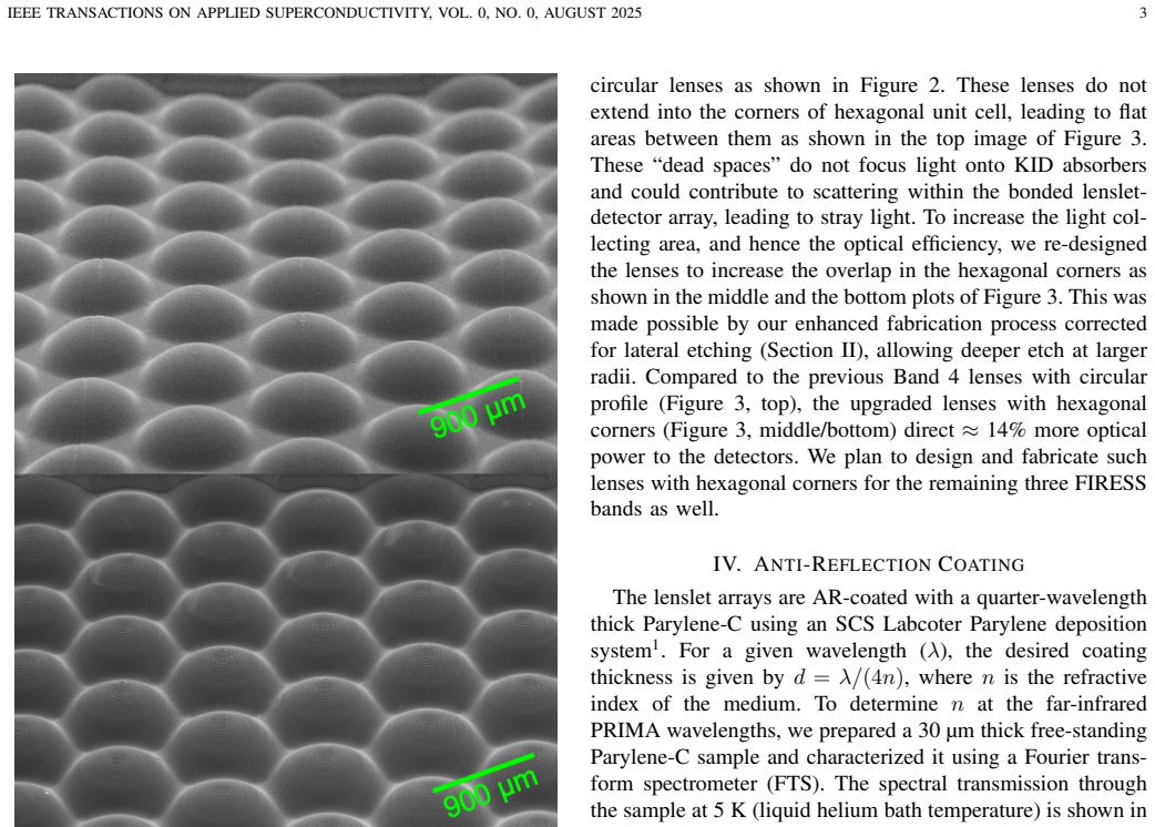
- [Section III (last paragraph)] The claim that the upgraded hexagonal-corner lenses 'direct ≈14% more optical power to the detectors' is presented as a quantitative result, but no derivation, simulation setup, ray-trace output, or measured throughput comparison is given. This number is load-bearing for the stated efficiency increase and for the value of the redesign. Please provide the supporting optical model (including the assumed focal-plane illumination, lens geometry, and absorber size) or a direct measurement, or adjust the claim to reflect an estimate based on geometric area only.
- [Sections IV and V (FTS extrapolation)] The FTS measured at a 5 K bath temperature are stated (Section IV) to represent the material's optical properties at the PRIMA operating temperature of 120 mK. This extrapolation is not justified. The AR-coating thicknesses (5 µm and 28 µm) and the bond-loss thresholds (<1 µm and <6 µm) are directly derived from these data. If the complex dielectric function of Parylene-C or epoxy changes between 5 K and 120 mK (e.g., from two-level systems or low-frequency phonon absorption), the coating and bond thickness requirements could shift, and the conclusion that the measured bond thicknesses 'meet the PRIMA requirements' would be insecure. Please provide a concrete argument for temperature insensitivity, low-temperature validation data, or quantitative uncertainty bounds on the FTS fits and their propagation to the thickness budgets.
- [Section III, Band 4 profile accuracy] Quantitative profile residuals are reported only for Band 1 (RMS <0.9 µm in Figure 2). For Band 4, the improved lens shape is shown in SEM and 3D profilometry, but no numerical comparison of the etched profile to the design (e.g., RMS residual, maximum deviation) is given. Since the paper claims the fabrication process meets FIRESS requirements for the extreme bands, and Band 4 required the lateral-etch compensation, the absence of a quantitative Band 4 profile error leaves the requirement verification incomplete. Please include a measured residual map or table for the Band 4 lenses.
- [Section V, bond-loss calculation] The derivation of the '5% loss' bond-thickness thresholds is not shown. The text states 'we calculated' and gives the resulting values (<1 µm for Band 1, <6 µm for Band 4) without presenting the model, the fringe- or absorption- loss formulation, or the material optical constants used. Because these thresholds are the basis for declaring the measured bond thicknesses compliant, please provide the calculation in sufficient detail to allow reproduction, or cite a publication containing it.
minor comments (5)
- [Section II] The statement that intermediate-band designs 'are expected to be relatively straightforward interpolations' is an assertion. Since the paper's title and abstract focus on PRIMA FIRESS generally, please either show a basis for this expectation (e.g., similarity of the two extreme designs) or explicitly cap the claim to Bands 1 and 4.
- [Section IV] The complex dielectric function fit is deferred to 'Wollack et al., in prep.' which is not accessible for review. At minimum, give the retrieved values of n and k (or loss tangent) and the uncertainty, so that the thickness calculations are reproducible.
- [Figure 4] No error bars or measurement uncertainties are shown on the FTS transmission spectra. Adding typical uncertainty envelopes (including thickness uncertainty of the free-standing samples) would strengthen the derived thickness budgets.
- [Abstract and Section IV] The abstract says 'demonstrate stepped-thickness AR-coatings to achieve high efficiency across broad wavelength ranges,' but the demonstration is a two-thickness test wafer, not a full four-step coating on a kilo-pixel array, and no optical efficiency measurement is reported. Please qualify the claim to 'process demonstration' and note that the final four-step arrays are under fabrication.
- [Section V] The destructive bond-thickness measurements are reported as ranges ('1–4 µm' for Band 4, '<1 µm' for Band 1) without stating the number of dies/locations measured or the measurement uncertainty. Adding this information would allow readers to judge the uniformity and reliability of the metrology.
Circularity Check
No circularity: every load-bearing result is a direct measurement or comparison to an independently derived threshold; the 5K-to-120mK extrapolation is a correctness risk, not a circular step.
full rationale
The paper's load-bearing results are direct measurements: profilometry residuals against design (Figure 2), SEM and 3D profilometry of etch depth (Figure 3), FTS spectra of free-standing Parylene-C and Epo-Tek 301 samples (Figure 4), and destructive sectioning to measure epoxy bond thickness (Section V). The etch-compensation model is fitted to etch data, but the claim that the process meets FIRESS requirements is validated by comparing final as-fabricated lens profiles to design, which is an independent check rather than a prediction from the fitted parameters. The AR-coating thicknesses and epoxy bond-thickness thresholds are computed from measured FTS transmission using standard quarter-wave and transmission-loss relations; the reported bond thicknesses are then compared to those thresholds, not generated by the same fit. Citations to [4] supply baseline process background and prior observations such as the lateral etching effect, but the present paper's conclusions do not reduce to [4] because the outcomes are measured here. The 5 K-to-120 mK extrapolation of material optical properties and the asserted interpolation to Bands 2 and 3 are unvalidated assumptions and correctness risks, but they are assumptions, not results equivalent to their inputs by construction. Therefore no circular step is present.
Axiom & Free-Parameter Ledger
free parameters (3)
- Isotropic etch fraction =
65–75%
- Parylene-C refractive index n(λ) =
1.66–1.68
- Epoxy bond force / thickness target =
<1 µm (Band 1), 1–4 µm (Band 4)
axioms (4)
- domain assumption FTS optical properties of Parylene-C and Epo-Tek 301 at 5 K equal the properties at 120 mK.
- standard math Quarter-wave AR-coating condition d=λ/(4n) is sufficient to compute near-unity transmission for the Parylene-C/silicon interface across each band.
- domain assumption The 65–75% isotropic-plus-anisotropic etch model describes grayscale/DRIE transfer at all radii including hexagonal corners.
- ad hoc to paper FIRESS Band 2 and Band 3 lenslet designs can be obtained by straightforward interpolation from Band 1 and Band 4.
read the original abstract
The PRobe far-Infrared Mission for Astrophysics (PRIMA) is a cryogenically cooled 1.8-m space telescope designed to address fundamental questions about the evolution of galactic ecosystems, the origins of planetary atmospheres, and the buildup of dust and metals over cosmic time. PRIMA will achieve unprecedented sensitivity in the 24 - 261 $\mu$m wavelength range, enabled by background-limited kinetic inductance detectors (KIDs) cooled to 120 mK. For PRIMA's Far-InfraRed Enhanced Survey Spectrometer (FIRESS) instrument, we have developed monolithic kilopixel silicon lenslet arrays to efficiently couple incident radiation from the telescope's fore-optics onto the KID absorber elements. These three-dimensional lenslet arrays are fabricated using grayscale lithography, followed by deep reactive ion etching (DRIE), and are anti-reflection (AR) coated with a quarter-wavelength thick deposition of Parylene-C. The lenslet arrays are aligned and bonded to the KID arrays using a thin layer of epoxy through a flip-chip bonder. In this work, we report on the optimized fabrication, lens design, AR coating, and bonding processes developed for the FIRESS lenslet arrays. We characterize brassboard lenslet arrays fabricated to meet the specifications of the FIRESS low and high spectral bands, demonstrate stepped-thickness AR-coatings to achieve high efficiency across broad wavelength ranges, and present spectral transmission measurements of the AR coating and the epoxy bonding layers.
Figures




Reference graph
Works this paper leans on
-
[1]
PRIMA: the probe far-infrared mission for astrophysics,
J. Glenn, M. Meixner, C. M. Bradford, K. M. Pontoppidan, E. A. Pope, T. Kataria, E. Luthman, M. C. Foote, M. B. Johnson, M. Cannella, A. M. Didion, R. Dissly, J. M. Rocca, J. K. Ziemer, L. Armus, J. Baselmans, C. Battersby, A. Bolatto, D. Burgarella, L. Ciesla, A. M. D. Giorgio, C. Gruppioni, T. Henning, O. Krause, B. S. Hensley, W. Jellema, E. Mills, A. ...
2024
-
[2]
A 25-micrometer single-photon-sensitive kinetic inductance detector,
P. K. Day, N. F. Cothard, C. Albert, L. Foote, E. Kane, B. H. Eom, R. Basu Thakur, R. M. J. Janssen, A. Beyer, P. M. Echternach, S. van Berkel, S. Hailey-Dunsheath, T. R. Stevenson, S. Dabironezare, J. J. A. Baselmans, J. Glenn, C. M. Bradford, and H. G. Leduc, “A 25-micrometer single-photon-sensitive kinetic inductance detector,” Phys. Rev. X, vol. 14, p...
-
[3]
Demonstration of ultrasensitive kids for future thz space borne polarimeters,
S. J. C. Yates, A. P. Laguna, W. Jellema, E. Castillo-Dominguez, L. Ferrari, B. Lap, V . Murugesan, J. R. G. Silva, D. Thoen, I. Veenendaal, and J. J. A. Baselmans, “Demonstration of ultrasensitive kids for future thz space borne polarimeters,”IEEE Transactions on Terahertz Science and Technology, vol. 15, no. 4, pp. 558–565, 2025. [Online]. Available: ht...
arXiv 2025
-
[4]
Monolithic silicon microlens arrays for far-infrared astrophysics,
N. F. Cothard, T. Stevenson, J. Mateo, N. Costen, K. Denis, J. Perido, I. Schrock, F. Wang, and J. Glenn, “Monolithic silicon microlens arrays for far-infrared astrophysics,” Appl. Opt., vol. 63, no. 6, p. 1481, Feb
-
[5]
The far-infrared enhanced survey spectrometer (FIRESS) for PRIMA,
C. M. Bradford, J. Glenn, M. Meixner, K. Pontoppidan, A. Kogut, A. Pope, W. Jellema, J. Baselmans, D. Naylor, R. Janssen, S. Hailey- Dunsheath, P. Echternach, P. Day, H. LeDuc, N. Cothard, T. Stevenson, M. Foote, C. D. Dowell, J. McGuire, M. Rodgers, T. S. Pagano, L. M. Foote, E. Kane, and C. Albert, “The far-infrared enhanced survey spectrometer (FIRESS)...
2024
-
[6]
PRIMA: PRIMAger, a far infrared hyperspectral and polarimetric instrument,
L. Ciesla, D. Burgarella, C. D. Dowell, M. Sauvage, J. Baselmans, C. M. Bradford, L. Ferrari, J. Floriot, J. Glenn, M. J. Griffin, W. Jellema, E. Luthman, L. Martin, T. Pamplona, ´E. Prieto, T. Prouv ´e, J. Staguhn, and C. Tucker, “PRIMA: PRIMAger, a far infrared hyperspectral and polarimetric instrument,” inSpace Telescopes and Instrumentation 2024: Opti...
2024
-
[7]
Feedhorn development and scalability for Simons Observatory and beyond,
S. M. Simon, J. E. Golec, A. Ali, J. Austermann, J. A. Beall, S. M. M. Bruno, S. K. Choi, K. T. Crowley, S. Dicker, B. Dober, S. M. Duff, E. Healy, C. A. Hill, S.-P. P. Ho, J. Hubmayr, Y . Li, M. Lungu, J. McMahon, J. Orlowski-Scherer, M. Salatino, S. Staggs, E. J. Wollack, Z. Xu, and N. Zhu, “Feedhorn development and scalability for Simons Observatory an...
2018
-
[8]
Design and testing of kinetic inductance detector package for the terahertz intensity mapper,
L. J. Liu, R. M. J. Janssen, C. M. Bradford, S. Hailey-Dunsheath, J. P. Filippini, J. E. Aguirre, J. S. Bracks, A. J. Corso, J. Fu, C. Groppi, J. Hoh, R. P. Keenan, I. N. Lowe, D. P. Marrone, P. Mauskopf, R. Nie, J. Redford, I. Trumper, and J. D. Vieira, “Design and testing of kinetic inductance detector package for the terahertz intensity mapper,” inMill...
2022
-
[9]
Dual- polarized sinuous antennas on extended hemispherical silicon lenses,
J. M. Edwards, R. O’Brient, A. T. Lee, and G. M. Rebeiz, “Dual- polarized sinuous antennas on extended hemispherical silicon lenses,” IEEE Transactions on Antennas and Propagation, vol. 60, no. 9, pp. 4082–4091, 2012. [Online]. Available: https://doi.org/10.1109/TAP. 2012.2207048
arXiv 2012
-
[10]
Flat Low-Loss Silicon Gradient Index Lens for Millimeter and Submillimeter Wavelengths,
F. Defrance, C. Jung-Kubiak, S. Rahiminejad, T. Macioce, J. Sayers, J. Connors, S. J. E. Radford, G. Chattopadhyay, and S. R. Golwala, “Flat Low-Loss Silicon Gradient Index Lens for Millimeter and Submillimeter Wavelengths,”Journal of Low Temperature Physics, vol. 199, no. 1-2, pp. 376–383, Apr. 2020. [Online]. Available: https://doi.org/10.1007/s10909-01...
-
[11]
B. Morgan, C. Waits, J. Krizmanic, and R. Ghodssi, “Development of a deep silicon phase fresnel lens using gray-scale lithography and deep reactive ion etching,”Journal of Microelectromechanical Systems, vol. 13, no. 1, pp. 113–120, 2004. [Online]. Available: https://doi.org/10.1109/JMEMS.2003.823220
arXiv 2004
-
[12]
Compensated aspect ratio dependent etching (carde) using gray-scale technology,
B. Morgan, C. M. Waits, and R. Ghodssi, “Compensated aspect ratio dependent etching (carde) using gray-scale technology,”Microelectronic Engineering, vol. 77, no. 1, pp. 85–94, 2005. [Online]. Available: https://doi.org/10.1016/j.mee.2004.09.004
-
[13]
B. Morgan and R. Ghodssi, “Design and simulation of comb-drive actuators incorporating gray-scale technology for tailored actuation characteristics,” inSmart Sensors, Actuators, and MEMS II, C. Cane, J.-C. Chiao, and F. V . Verdu, Eds., vol. 5836, International Society for Optics and Photonics. SPIE, 2005, pp. 468 – 476. [Online]. Available: https://doi.o...
-
[2024]
Available: https://doi.org/10.1364/AO.510409
[Online]. Available: https://doi.org/10.1364/AO.510409
discussion (0)
Sign in with ORCID, Apple, or X to comment. Anyone can read and Pith papers without signing in.