REVIEW 4 major objections 4 minor 20 references
Fabrication of p+ contact by thermally induced solid state regrowth of Al on p-type Ge crystal
T0 review · 4 major / 4 minor · reviewed 2026-08-14 · deepseek-v4-flash
Pith's one-line read Annealing a thermally deposited aluminum film on p-type germanium at 350°C produces a rugged p+ contact by solid-state regrowth, with aluminum penetrating to roughly four times the film thickness.
desk verdict Solid process-engineering follow-up on a 1970s contact technique, with a plausible but under-verified thickness-scaling claim. read the letter →
The pith
A machine-rendered reading of the paper's core claim, the machinery that carries it, and where it could break.
The reading
What carries the argument
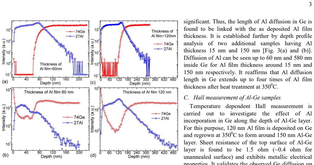
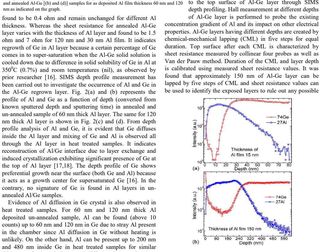
The central mechanism is solid-state regrowth by layer exchange. At 350°C Ge diffuses into the Al film (solid solubility about 0.7%) and, on slow cooling, the supersaturated Ge regrows on the Ge crystal while carrying Al into the crystal. The as-deposited Al thickness acts as the control parameter for the final contact: the paper's SIMS data indicate the Al penetration depth into Ge is roughly four times that thickness. To map the concentration gradient, the paper combines SIMS depth profiling with Hall measurements on surfaces exposed by repeated chemical-mechanical lapping.
What would settle it
A cross-sectional transmission electron microscope scan with elemental mapping through the annealed interface would settle it: if the Al-rich region does not extend roughly four times the Al film thickness into the Ge crystal, the SIMS-based claim is wrong; repeating the SIMS on unannealed samples at lower sputter energy would reveal whether the apparent Al tail is an artifact.
Extended reading notes
Core claim
On its own terms, the paper establishes that thermally depositing Al on p-type Ge and annealing at 350°C, below the Al-Ge eutectic of 424°C, then cooling slowly, gives a recrystallized Al-Ge layer with a p+/p doping profile. SIMS depth profiles show Ge present through the whole Al layer after annealing but absent from unannealed films, which the authors read as layer exchange and solid-phase regrowth. The same profiles show Al inside the Ge crystal to depths of about four times the as-deposited Al film thickness, for example roughly 200 nm for 60 nm Al and 480 nm for 120 nm Al. Hall measurements after successive lapping show the top surface is metallic, with Al concentrations near $10^{20}\,\mathrm{cm^{-3}}$ falling to about $10^{11}\,\mathrm{cm^{-3}}$ toward the bulk, so the contact is p+ at the surface and p-type below.
Load-bearing premise
The quantitative diffusion-length claim rests on reading the Al signal in unannealed SIMS profiles as stray contamination rather than as a measurement artifact; if that baseline is wrong, the reported 'four times the Al film thickness' depth is not supported.
Editorial extensions
If this is right
- Ge diode detectors could be fitted with p+ contacts by evaporation and annealing, replacing boron ion implantation and the associated apparatus.
- The depth of the p+ region can be tuned by choosing the aluminum film thickness, since the paper reports Al penetration scales as about four times that thickness.
- The top surface of the regrown Al-Ge layer has low sheet resistance, so the contact can serve directly for electrical readout in a detector.
- Because the doping falls off from p+ to p-type, the contact forms a graded hole-selective region rather than an abrupt junction, with carrier concentrations from about $10^{19}$–$10^{20}\,\mathrm{cm^{-3}}$ down to about $10^{11}\,\mathrm{cm^{-3}}$.
- Since the anneal stays below the Al-Ge eutectic, the contact forms without melting, which keeps the process compatible with other low-temperature device steps.
Reading between the lines
- The four-times scaling was tested for Al films from 15 nm to 150 nm with a fixed 40-minute anneal; whether it holds for thicker films or longer anneal times is untested and would be a natural next measurement.
- If the same regrowth works on n-type Ge, the p+ contact could serve as the hole-blocking or anode contact in a full detector diode, extending the method beyond p-type substrates.
- The paper's interpretation of the unannealed Al tail as stray chamber contamination is directly testable by comparing SIMS profiles taken at different sputter energies; a persistent tail would point to ion-beam mixing instead.
- A cross-sectional microscopy measurement of the annealed interface could independently confirm both the depth and the shape of the Al distribution implied by the SIMS profiles.
Signed reviews
Editorial analysis
A structured set of objections, weighed in public.
Referee Report
Summary. The manuscript reports fabrication of p+ contacts on p-type Ge crystals by thermal evaporation of Al followed by annealing at 350°C and slow cooling. The authors use SIMS depth profiling to argue that Ge diffuses through the entire Al layer and that Al diffuses into Ge to a depth of approximately four times the as-deposited Al film thickness. Hall measurements on progressively lapped Al-Ge layers are used to infer an Al concentration gradient and p+/p doping profile. The paper claims that the regrown contact layer is rugged and that its thickness can be controlled by the deposited Al thickness. The central quantitative claims are the four-times diffusion scaling and top-surface Al dopant concentrations near 10^20/cm3.
Significance. If the results hold, the paper offers a simple, low-temperature route to p+ contacts on Ge, relevant to detector and electronic device applications. The systematic variation of Al film thickness and the combination of SIMS and Hall measurements are strengths. The paper builds on a known solid-phase regrowth approach and adds a claimed thickness control law. However, the quantitative claims rest on a small number of single measurements and on a SIMS baseline interpretation that is not adequately controlled. The qualitative picture of interdiffusion and p-type doping is plausible, but the load-bearing 'four times thickness' scaling and the reported concentration values need stronger support.
major comments (4)
- [III.B, Figs. 2 and 3] The unannealed Al/Ge SIMS profiles already show Al tails extending 60 nm and 120 nm into Ge, which the authors attribute to stray Al in the evaporation chamber rather than to room-temperature diffusion. This attribution is asserted without a control measurement on an Al-free Ge sample or an assessment of SIMS artifacts such as ion-beam mixing, knock-on, or crater/interface roughening. Because the annealed diffusion depths (200 nm and 480 nm for 60 nm and 120 nm Al, respectively; 60 nm and 580 nm for 15 nm and 150 nm Al) are read from the same kind of raw tail, any such artifact would contribute to every annealed profile. The appropriate thermal diffusion depth would then be the annealed-minus-unannealed excess, roughly 3t rather than 4t, and the linear scaling with film thickness would not be established. This directly affects the central claim that the regrown layer length is controlled by the as-deposited Al thickness.
- [III.B, Fig. 5(b) and Conclusion] The text states that the Al concentration on the top surface of the regrown Al-Ge layer is 'as high as 10^23/cc' for 120 nm Al, while the Conclusion states that 'Dopant concentration at the top surface ... can be as high as 10^20/cm3.' These values differ by three orders of magnitude. The Hall data in Fig. 4(b) additionally give carrier concentrations near 10^19/cm3 for the 15 ohm sheet resistance layer. The manuscript must reconcile these numbers; as written, the reported Al concentration values are internally inconsistent and the claimed p+ doping level is not reliably quantified.
- [III.B, Hall measurement and depth calibration] The depth calibration for the lapped Hall measurements uses sheet resistance values: 'Duration of the CML is calibrated using measured sheet resistance values.' Since sheet resistance is then reported as the dependent variable versus depth, using the same values to assign depths risks circularity. The total lapped depth is stated as approximately 150 nm, but individual depth values plotted in Fig. 4(a) are not independently verified by profilometry or another technique. Please provide independent depth measurements at each CML step or state clearly that the depth axis is inferred from the sheet resistance calibration.
- [III.B, Figs. 2-5] No error bars, replicate measurements, or uncertainty analysis are provided for the SIMS profiles, diffusion lengths, sheet resistances, carrier concentrations, or Hall coefficients. All quantitative conclusions rest on single measurements per condition. Given the observed variability in electrical data (e.g., 1.5 ohm for 120 nm Al versus 7 ohm for 30 nm Al), the paper should report statistics from at least three samples per condition or explicitly justify why a single measurement is representative.
minor comments (4)
- [III.B, SIMS threshold] The statement 'Al can be found (above 10 counts) up to 60 nm and 120 nm in Ge' does not define the threshold or its units; please specify the detection limit or background level used to define the diffusion depth.
- [Throughout] The text contains inconsistent notation, such as '0C' instead of '°C', and inconsistent use of 'Al/Ge' for unannealed and 'Al-Ge' for annealed samples; please standardize these conventions.
- [III.B, conductivity transition discussion] The discussion of the extrinsic-to-intrinsic transition and its shift with Al concentration is difficult to follow; a figure or a more explicit explanation of the carrier compensation and mobility effects would improve clarity.
- [I, Introduction] The reference to 'A1' (Al) and 'AI' appears multiple times; please correct these typographical errors.
Circularity Check
No significant circularity: the paper's central claims are direct experimental measurements, not derived from fitted inputs or self-citation chains.
full rationale
The paper's central claims—Al/Ge interdiffusion at 350 C, Ge transport through the Al film, Al penetration into Ge scaling with film thickness, and the resulting p+/p doping gradient—are obtained directly from SIMS depth profiles and Hall/sheet-resistance measurements. No parameter is fitted to a subset of data and then repackaged as a prediction; the 'four times film thickness' rule is a read-out of measured SIMS tails, with the caveat that the unannealed baseline also shows tails equal to the film thickness, which is a measurement-interpretation concern (possible SIMS mixing or stray Al) rather than a circularity. The only quasi-inferential loop, using sheet resistance values to help identify lapped depths, is anchored by an independent total-layer-depth estimate of roughly 150 nm obtained from profilometry and SIMS crater depths, and it does not enter the central diffusion-length or doping-gradient claims. Reference [19] is a self-citation used for a peripheral comparison of transition-temperature shifts; it is not load-bearing, and it reports independent experimental data rather than an unverified assumption. Therefore the derivation chain is self-contained and no circular step is exhibited.
Assumptions & free parameters
free parameters (1)
- Al diffusion depth proportionality constant =
~4 (measured 3.3 to 4.0 for Al films of 15, 60, 120, and 150 nm)
assumptions (7)
- domain assumption Solid-state regrowth of Al on Ge below the eutectic temperature (424 degrees Celsius) produces epitaxial p-type Al-Ge contacts
- domain assumption Ge solid solubility in Al is about 0.7% at 350 degrees Celsius and near zero at room temperature, driving supersaturation and regrowth during slow cooling
- domain assumption SIMS sputter time converts linearly to depth using measured crater depths
- ad hoc to paper Al diffusion in Ge at room temperature is negligible, so the Al tail in unannealed samples is stray Al from the evaporation chamber
- domain assumption Hall-measured carrier concentration equals the electrically active Al concentration
- domain assumption CML removes uniform layers and sheet resistance can identify the exposed depth
- domain assumption The p-type Ge substrate has carrier concentration about 10^10 per cubic centimeter at 77K and shows extrinsic-to-intrinsic transition near 220-260K
Cite this review
Pith. "Pith review of Fabrication of p+ contact by thermally induced solid state regrowth of Al on p-type Ge crystal." pith.science (2026). https://pith.science/paper/FVXS6WUR
@misc{pith2026190803036,
  author       = {Pith},
  title        = {Pith review of: Fabrication of p+ contact by thermally induced solid state regrowth of Al on p-type Ge crystal},
  year         = {2026},
  howpublished = {\url{https://pith.science/paper/FVXS6WUR}},
  note         = {Machine review of arXiv:1908.03036}
}
read the original abstract
Formation of p+ contact on Germanium is important for applications in diode detector and other electronic devices. In this work, thermally deposited Al on Ge crystal is annealed at 350oC followed by slow cooling for solid-state regrowth of Al-Ge p+ contact on Ge. Depth profile analysis by secondary ion mass spectrometry (SIMS) is carried out to investigate the occurrence of Al and Ge along the depth of the regrown Al-Ge layer. Evidence of regrowth is observed due to inter-diffusion of both Ge and Al across the layers although Ge diffusion in Al layer is found to be more prevalent. Thickness of the evaporated Al layer is varied to understand the diffusion profile of Al, Ge and estimate the depth of Al incorporation in Ge crystal underneath. Hall measurement at different depth of Al-Ge regrown layer reveals that Al impurity induces p+ doping in p-type Ge and its concentration gradually reduces towards the Ge crystal. Top surface of the Al-Ge layer exhibits lowest sheet resistance that varies with the thickness of the as deposited Al layer.
Figures

Figures from the paper (2 more)


Reference graph
Works this paper leans on
-
[1]
Germanium gamma-ray detectors,
R. H. Pehl, “Germanium gamma-ray detectors,” Physics Today, vol. 30, no. 11, p. 50, 1977
work page 1977
-
[2]
Gamma ray detectors made from high purity germanium,
R. D. Baertsch and R. N. Hall, “Gamma ray detectors made from high purity germanium,” IEEE Transactions on Nuclear Science, vol. 17, no. 3, pp. 235-240, 1970
work page 1970
-
[3]
J. Eberth and J. Simpson, “From Ge(Li) detectors to gamma-ray tracking arrays–50 years of gamma spectroscopy with germanium detectors,” Progress in Particle and Nuclear Physics, vol. 60, no. 2, pp. 283-337, 2008
work page 2008
-
[4]
Formation of injecting and blocking contacts on high-resistivity germanium,
G. Ottaviani, V. Marrello, J. W. Mayer, M-A. Nicolet, and J. M. Caywood, “Formation of injecting and blocking contacts on high-resistivity germanium,” Appl. Phys. Lett., vol. 20, pp. 323-325, 1972
work page 1972
-
[5]
R. H. Pehl and R. C. Cordi, “Lithium-diffused n+ contacts on high-purity germanium detectors: How thin can they be made-how stable are they?” IEEE Transaction on Nuclear Science, vol. 22, no. 1, pp. 177-177, 1975
work page 1975
-
[6]
Diffusion of boron in germanium at 800-9000C,
S. Uppal, A. F. W. Willoughby, J. M. Bonar, N. E. B. Cowern, T. Grasby, R. J. H. Morris, and M. G. Dowsett, “Diffusion of boron in germanium at 800-9000C,” J. Appl. Phys., vol. 96, pp. 1376-1380, 2004
work page 2004
-
[7]
Leakage current in high-purity germanium detectors with amorphous semiconductor contacts,
Q. Looker, M. Amman and K.Vetter, “Leakage current in high-purity germanium detectors with amorphous semiconductor contacts,” Nuclear Instruments and Methods in Physics Research A, vol. 777, pp. 138-147, 2015
work page 2015
-
[8]
X.-H. Meng, G.-J. Wang, M.-D. Wagner, H. Mei, W.-Z. Wei, J. Liu, G. Yang, and D.-M. Mei, “Fabrication and characterization of high-purity germanium detectors with amorphous germanium contacts,” Journal of Instrumentation, vol. 14, no. 2, pp. P02019, Feb. 2019
work page 2019
Show all 20 references
-
[9]
Thin film reaction of transition metals with germanium,
S. Gaudet, C. Detavernier, A. J. Kellock, P. Desjardins, and C. Lavoie, “Thin film reaction of transition metals with germanium,” J. of Vac. Sci. & Tech. A, vol. 24, pp. 474- 485, 2006
2006
-
[10]
Low temperature migration of silicon in thin layers of gold and platinum,
A. Hiraki, M-A. Nicolet, and J. W. Mayer, “Low temperature migration of silicon in thin layers of gold and platinum,” Appl. Phys. Letters., vol. 18, no. 5, pp. 178-181, 1971
1971
-
[11]
Alloying behavior of Au and Au–Ge on GaAs,
J. Gyulai, J. W. Mayer, V. Rodriguez, A.Y.C. Yu, and H. J. Gopen, “Alloying behavior of Au and Au–Ge on GaAs,” J. Appl. Phys., vol. 42, no. 9, 3578-3585, 1971
1971
-
[12]
Solid-phase epitaxial growth of Ge layers,
V. Marrelloj, M. Caywood, J. W. Mayer, and M.-A. Nicole, “Solid-phase epitaxial growth of Ge layers,” phys. stat. sol. (a), vol. 13, pp. 531-536, 1972
1972
-
[13]
Solid-phase growth of Ge from evaporated Al Layer,
J. M. Caywood, A. M. Fern, J.O. McCaldin, and G. Ottaviani, “Solid-phase growth of Ge from evaporated Al Layer,” Appl. Phys. Lett., vol. 20, pp. 326-327, 1972
1972
-
[14]
Germanium alpha particle detectors with aluminum regrowth p+ contacts,
A. Lidow, “Germanium alpha particle detectors with aluminum regrowth p+ contacts,” Nuclear Instruments and Methods, vol. 124, pp. 609-610, 1975
1975
-
[15]
High purity germanium gamma-ray spectrometers with regrowth p+ contacts,
V. Marrello, T. A. McMath, J.W. Mayer and I. L. Fowler, “High purity germanium gamma-ray spectrometers with regrowth p+ contacts,” Nuclear Instruments and Methods, vol. 108, pp. 93-97, 1973
1973
-
[16]
Some aspects of Ge epitaxial growth by solid solution,
G. Ottaviani, C. Canali, and G. Majni, “Some aspects of Ge epitaxial growth by solid solution,” Journal of Applied Physics, vol. 47, no. 2, pp. 627-630, 1976
1976
-
[17]
Nucleation and growth kinetics during metal-induced layer exchange crystallization of Ge thin films at low temperatures,
S. Hu and P. C. McIntyre, “Nucleation and growth kinetics during metal-induced layer exchange crystallization of Ge thin films at low temperatures,” J. Appl. Phys., Vol. 111, no. 4, p. 044908, 2012
2012
-
[18]
Sigurd, G
D. Sigurd, G. Ottaviani, H. J. Arnal, and J. W. Mayer, Crystallization of Ge and Si in metal films. II,” J. of Appl. Phys., vol. 45, no. 4, pp. 1740-1745, 1974
1974
-
[19]
Impurity concentration dependent electrical conduction in germanium crystal at low temperatures,
M. Ghosh, S. Pitale, S. G. Singh, S. Sen, S. C. Gadkari, “Impurity concentration dependent electrical conduction in germanium crystal at low temperatures,” Bulletin of Materials Science (accepted), arXiv:1907.05067 [cond- mat.mtrl-sci]
1907 arXiv
-
[20]
Aluminium implantation in germanium: Uphill diffusion, electrical activation, and trapping,
G. Impellizzeri, E. Napolitani, S. Boninelli, V. Privitera, T. Clarysse, W. Vandervorst, and F. Priolo, “Aluminium implantation in germanium: Uphill diffusion, electrical activation, and trapping,” Applied Physics Express, vol. 5, no. 2, pp. 021301-3, 2012
2012
Reviewed August 14, 2026 · model on record in the stance chip above.
Discussion (0). Continue with ORCID to comment.