Superconducting cavity probes sliding ferroelectricity in small-angle twisted WSe₂
Pith reviewed 2026-06-26 11:30 UTC · model grok-4.3
The pith
Embedding small-angle twisted WSe2 in a superconducting cavity detects sliding ferroelectric switching via hysteretic capacitance and quality factor.
A machine-rendered reading of the paper's core claim, the machinery that carries it, and where it could break.
Core claim
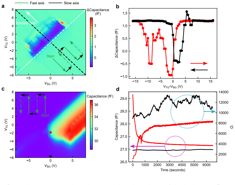
Placing a small-angle parallel-stacked WSe2 bilayer inside a half-wave superconducting coplanar waveguide cavity allows the high-frequency AC response of the stack to be measured; the resulting data exhibit hysteresis in both capacitance and cavity quality factor, directly confirming ferroelectric switching, together with relaxation processes attributed to domain-wall motion.
What carries the argument
The half-wave superconducting coplanar waveguide cavity that converts changes in the bilayer's out-of-plane polarization into measurable shifts in capacitance and resonator quality factor.
If this is right
- Ferroelectric domain switching produces detectable changes in both the real and imaginary parts of the high-frequency admittance of the bilayer.
- Domain-wall motion introduces a distinct relaxation time scale visible in the frequency-dependent response of the cavity.
- The same cavity geometry can in principle be used to track domain dynamics in other sliding-ferroelectric 2D systems without requiring direct electrical contacts to the active layer.
Where Pith is reading between the lines
- Because the cavity operates at radio frequencies, the method may separate fast electronic contributions from slower ionic or domain-wall contributions more cleanly than quasi-static capacitance measurements.
- Integration of multiple cavities on the same chip could allow spatially resolved mapping of domain configurations if the resonator mode volume is made smaller than the typical domain size.
- The technique might be combined with gate tuning to map the dependence of domain-wall mobility on carrier density in the same device.
Load-bearing premise
The observed hysteresis and relaxation arise specifically from ferroelectric domain switching and domain-wall motion rather than from unrelated mechanisms such as charge trapping, leakage currents, or heating.
What would settle it
Repeating the cavity measurements on control devices that contain only untwisted or antiparallel WSe2 bilayers (expected to lack sliding ferroelectricity) and finding no hysteresis would falsify the claim that the signal originates from sliding ferroelectric switching.
Figures
read the original abstract
Ferroelectricity is a property of materials that exhibit spontaneous charge polarization. Ferroelectricity in 2D materials is interesting because of their applications in memory devices and field-effect transistors. Recently, a new type of ferroelectricity, known as sliding ferroelectricity, has been discovered, in which parallel-stacked bilayers of hexagonal boron nitride (hBN) or transition metal dichalcogenides (TMDCs) develop an out-of-plane electric polarization. In this work, we probe the polarization of small-angle parallel stacked WSe$_2$ by measuring its high-frequency AC response, achieved by embedding it into a half-wave superconducting coplanar waveguide cavity. We observe a hysteretic response in the capacitance of the stack and quality factor of the cavity, confirming ferroelectric switching in the system. Our results further reveal relaxation effects associated with ferroelectric domain-wall motion. This cavity-based technique has potential applications in probing domain-wall dynamics in a ferroelectric system at high frequencies.
Editorial analysis
A structured set of objections, weighed in public.
Referee Report
Summary. The manuscript describes embedding small-angle twisted WSe₂ bilayers into a half-wave superconducting coplanar waveguide cavity to measure the high-frequency AC response. The central experimental claim is the observation of hysteretic behavior in the extracted capacitance of the stack and the cavity quality factor, which the authors interpret as direct confirmation of sliding ferroelectric switching; they additionally report relaxation effects attributed to ferroelectric domain-wall motion. The work positions the cavity technique as a probe for high-frequency domain dynamics in 2D ferroelectrics.
Significance. If the mapping from cavity observables to ferroelectric polarization is robust, the approach supplies a contactless, high-frequency method for studying sliding ferroelectricity and domain-wall dynamics that is complementary to DC transport or PFM measurements. This could be useful for characterizing 2D ferroelectric memory elements where switching speed and relaxation are relevant.
major comments (3)
- [Results] Results section (hysteresis data): the attribution of the observed capacitance and Q-factor hysteresis loops specifically to sliding ferroelectric domain switching and domain-wall relaxation is not supported by explicit controls that would exclude alternative mechanisms such as interface charge trapping, leakage currents, or RF-induced heating. No temperature dependence of the coercive voltage, frequency scaling of the relaxation time, or measurements on non-ferroelectric reference stacks (e.g., large-angle or monolayer devices) are described.
- [Methods] Methods / device fabrication: the manuscript provides no quantitative comparison between the extracted coercive fields or polarization values and literature values for sliding ferroelectricity in twisted WSe₂, nor does it report the RF power levels used or any check that the drive remains in the linear regime where heating or nonlinear leakage would be negligible.
- [Discussion] Discussion of relaxation: the claim that the observed relaxation timescales arise from domain-wall motion rests on the untested assumption that competing relaxation channels (e.g., trap emission or dielectric relaxation) produce neither the reported loop shape nor the same time constants; no supporting data or modeling is supplied to discriminate these possibilities.
minor comments (2)
- [Abstract] The abstract states both 'parallel-stacked' and 'small-angle twisted' WSe₂; the relationship between these descriptions should be clarified in the introduction.
- [Figures] Figure captions for the cavity response data should explicitly state the fitting procedure used to extract capacitance and Q, including any background subtraction or calibration steps.
Simulated Author's Rebuttal
We thank the referee for their careful reading and constructive comments on our manuscript. We address each major comment below and indicate where revisions will be made.
read point-by-point responses
-
Referee: [Results] Results section (hysteresis data): the attribution of the observed capacitance and Q-factor hysteresis loops specifically to sliding ferroelectric domain switching and domain-wall relaxation is not supported by explicit controls that would exclude alternative mechanisms such as interface charge trapping, leakage currents, or RF-induced heating. No temperature dependence of the coercive voltage, frequency scaling of the relaxation time, or measurements on non-ferroelectric reference stacks (e.g., large-angle or monolayer devices) are described.
Authors: We agree that additional controls would strengthen the attribution to ferroelectric switching. The manuscript does not contain temperature-dependent measurements, frequency scaling data, or reference stack experiments. We will revise the Results and Discussion sections to explicitly address why alternative mechanisms (trapping, leakage, heating) are inconsistent with the simultaneous hysteresis in both capacitance and Q-factor, based on the observed loop shapes and timescales. New control experiments are not feasible within this revision. revision: partial
-
Referee: [Methods] Methods / device fabrication: the manuscript provides no quantitative comparison between the extracted coercive fields or polarization values and literature values for sliding ferroelectricity in twisted WSe₂, nor does it report the RF power levels used or any check that the drive remains in the linear regime where heating or nonlinear leakage would be negligible.
Authors: We will revise the Methods section to report the RF power levels used in the measurements and to include a check confirming operation in the linear regime (via drive-amplitude scaling). We will also add a quantitative comparison of the extracted coercive fields and polarization values to existing literature reports on sliding ferroelectricity in twisted WSe₂. revision: yes
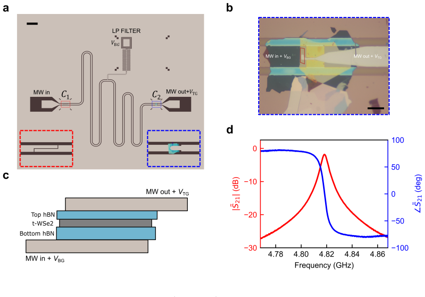
-
Referee: [Discussion] Discussion of relaxation: the claim that the observed relaxation timescales arise from domain-wall motion rests on the untested assumption that competing relaxation channels (e.g., trap emission or dielectric relaxation) produce neither the reported loop shape nor the same time constants; no supporting data or modeling is supplied to discriminate these possibilities.
Authors: We will expand the Discussion to include references to literature on competing relaxation channels and provide a qualitative discrimination based on the specific loop shape and time constants observed. Supporting modeling of the relaxation dynamics will be added to the supplementary information. revision: yes
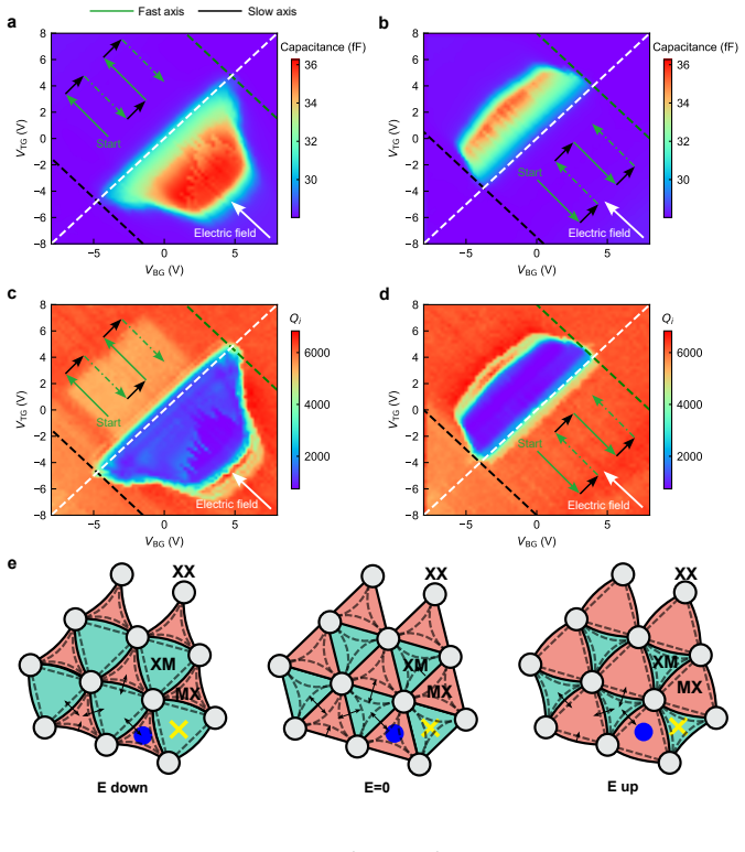
- Temperature dependence of the coercive voltage
- Frequency scaling of the relaxation time
- Measurements on non-ferroelectric reference stacks (large-angle or monolayer devices)
Circularity Check
No circularity: direct experimental observation without derivations or self-referential steps
full rationale
The manuscript is an experimental report of hysteretic capacitance and cavity Q-factor in a twisted WSe2 stack embedded in a superconducting cavity. No derivation chain, fitted parameters renamed as predictions, self-citations as load-bearing uniqueness theorems, or ansatzes smuggled via prior work appear in the abstract or described structure. The central claim rests on raw measurement of hysteresis and relaxation, with interpretation left open to alternative mechanisms; this is an empirical mapping, not a reduction of output to input by construction. The paper is self-contained against external benchmarks as a measurement report.
Axiom & Free-Parameter Ledger
Reference graph
Works this paper leans on
-
[1]
L. W. Martin and A. M. Rappe, Thin-film ferroelectric materials and their applications, Nature Reviews Materials2, 16087 (2016)
2016
-
[2]
R. Guo, L. You, Y. Zhou, Z. Shiuh Lim, X. Zou, L. Chen, R. Ramesh, and J. Wang, Non-volatile memory based on the ferroelectric photovoltaic effect, Nature Communications 4, 1990 (2013)
1990
-
[3]
A. I. Khan, A. Keshavarzi, and S. Datta, The future of ferroelectric field-effect transistor technology, Nature Electronics3, 588 (2020)
2020
-
[4]
H. Jiao, X. Wang, S. Wu, Y. Chen, J. Chu, and J. Wang, Ferroelectric field effect transistors for electronics and optoelectronics, Applied Physics Reviews10, 011310 (2023)
2023
-
[5]
Y. He, B. Bahr, M. Si, P. Ye, and D. Weinstein, A tunable ferroelectric based unreleased RF resonator, Microsystems & Nanoengineering6, 8 (2020)
2020
-
[6]
F. Mao, J. Gui, Y. Hou, S. Gao, H. Zeng, W. Wang, Z. Xu, Y. Zhu, L. Fan, and H. Zhang, Ultra-tunable dielectric capacitors enhanced by coupling ferroelectric field effect and semiconductor field effect, Applied Physics Letters125, 223502 (2024)
2024
-
[7]
von Hippel, Ferroelectricity, Domain Structure, and Phase Transitions of Barium Titanate, Reviews of Modern Physics22, 221 (1950)
A. von Hippel, Ferroelectricity, Domain Structure, and Phase Transitions of Barium Titanate, Reviews of Modern Physics22, 221 (1950)
1950
-
[8]
V. G. Bhide, M. S. Hegde, and K. G. Deshmukh, Ferroelectric Properties of Lead Titanate, Journal of the American Ceramic Society51, 565 (1968)
1968
-
[9]
Junquera and P
J. Junquera and P. Ghosez, Critical thickness for ferroelectricity in perovskite ultrathin films, Nature422, 506 (2003)
2003
-
[10]
Dawber, K
M. Dawber, K. M. Rabe, and J. F. Scott, Physics of thin-film ferroelectric oxides, Reviews of Modern Physics77, 1083 (2005)
2005
-
[11]
Zheng, L
C. Zheng, L. Yu, L. Zhu, J. L. Collins, D. Kim, Y. Lou, C. Xu, M. Li, Z. Wei, Y. Zhang, M. T. Edmonds, S. Li, J. Seidel, Y. Zhu, J. Z. Liu, W.-X. Tang, and M. S. Fuhrer, Room temperature in-plane ferroelectricity in van der Waals In 2Se3, Science Advances4, eaar7720 (2018)
2018
-
[12]
F. Liu, L. You, K. L. Seyler, X. Li, P. Yu, J. Lin, X. Wang, J. Zhou, H. Wang, H. He, S. T. Pantelides, W. Zhou, P. Sharma, X. Xu, P. M. Ajayan, J. Wang, and Z. Liu, Room-temperature ferroelectricity in CuInP 2S6 ultrathin flakes, Nature Communications7, 12357 (2016). 16
2016
-
[13]
Z. Fei, W. Zhao, T. A. Palomaki, B. Sun, M. K. Miller, Z. Zhao, J. Yan, X. Xu, and D. H. Cobden, Ferroelectric switching of a two-dimensional metal, Nature560, 336 (2018)
2018
-
[14]
Y. Wan, T. Hu, X. Mao, J. Fu, K. Yuan, Y. Song, X. Gan, X. Xu, M. Xue, X. Cheng, C. Huang, J. Yang, L. Dai, H. Zeng, and E. Kan, Room-temperature ferroelectricity in 1t′-res2 multilayers, Physical Review Letters128, 067601 (2022)
2022
-
[15]
W. Cao, O. Hod, and M. Urbakh, Interlayer Registry Dictates Interfacial 2D Material Ferroelectricity, ACS Applied Materials & Interfaces14, 57492 (2022)
2022
-
[16]
Liang, D
J. Liang, D. Yang, J. Wu, J. Dadap, K. Watanabe, T. Taniguchi, and Z. Ye, Optically Probing the Asymmetric Interlayer Coupling in Rhombohedral-Stacked MoS2 Bilayer, Physical Review X12, 041005 (2022)
2022
-
[17]
Li and M
L. Li and M. Wu, Binary Compound Bilayer and Multilayer with Vertical Polarizations: Two-Dimensional Ferroelectrics, Multiferroics, and Nanogenerators, ACS Nano11, 6382 (2017)
2017
-
[18]
Yasuda, X
K. Yasuda, X. Wang, K. Watanabe, T. Taniguchi, and P. Jarillo-Herrero, Stacking-engineered ferroelectricity in bilayer boron nitride, Science372, 1458 (2021)
2021
-
[19]
Vizner Stern, Y
M. Vizner Stern, Y. Waschitz, W. Cao, I. Nevo, K. Watanabe, T. Taniguchi, E. Sela, M. Urbakh, O. Hod, and M. Ben Shalom, Interfacial ferroelectricity by van der Waals sliding, Science372, 1462 (2021)
2021
-
[20]
Weston, E
A. Weston, E. G. Castanon, V. Enaldiev, F. Ferreira, S. Bhattacharjee, S. Xu, H. Corte-Le´ on, Z. Wu, N. Clark, A. Summerfield, T. Hashimoto, Y. Gao, W. Wang, M. Hamer, H. Read, L. Fumagalli, A. V. Kretinin, S. J. Haigh, O. Kazakova, A. K. Geim, V. I. Fal’ko, and R. Gorbachev, Interfacial ferroelectricity in marginally twisted 2D semiconductors, Nature Na...
2022
-
[21]
X. Wang, K. Yasuda, Y. Zhang, S. Liu, K. Watanabe, T. Taniguchi, J. Hone, L. Fu, and P. Jarillo-Herrero, Interfacial ferroelectricity in rhombohedral-stacked bilayer transition metal dichalcogenides, Nature Nanotechnology17, 367 (2022)
2022
-
[22]
S. Deb, W. Cao, N. Raab, K. Watanabe, T. Taniguchi, M. Goldstein, L. Kronik, M. Urbakh, O. Hod, and M. Ben Shalom, Cumulative polarization in conductive interfacial ferroelectrics, Nature612, 465 (2022)
2022
-
[23]
K. Ko, A. Yuk, R. Engelke, S. Carr, J. Kim, D. Park, H. Heo, H.-M. Kim, S.-G. Kim, H. Kim, T. Taniguchi, K. Watanabe, H. Park, E. Kaxiras, S. M. Yang, P. Kim, and H. Yoo, 17 Operando electron microscopy investigation of polar domain dynamics in twisted van der Waals homobilayers, Nature Materials22, 992 (2023)
2023
-
[24]
T. H. Yang, B.-W. Liang, H.-C. Hu, F.-X. Chen, S.-Z. Ho, W.-H. Chang, L. Yang, H.-C. Lo, T.-H. Kuo, J.-H. Chen, P.-Y. Lin, K. B. Simbulan, Z.-F. Luo, A. C. Chang, Y.-H. Kuo, Y.-S. Ku, Y.-C. Chen, Y.-J. Huang, Y.-C. Chang, Y.-F. Chiang, T.-H. Lu, M.-H. Lee, K.-S. Li, M. Wu, Y.-C. Chen, C.-L. Lin, and Y.-W. Lan, Ferroelectric transistors based on shear-tran...
2024
-
[25]
Liang, D
J. Liang, D. Yang, Y. Xiao, S. Chen, J. I. Dadap, J. Rottler, and Z. Ye, Shear Strain-Induced Two-Dimensional Slip Avalanches in Rhombohedral MoS 2, Nano Letters23, 7228 (2023)
2023
-
[26]
S. C. de la Barrera, Q. Cao, Y. Gao, Y. Gao, V. S. Bheemarasetty, J. Yan, D. G. Mandrus, W. Zhu, D. Xiao, and B. M. Hunt, Direct measurement of ferroelectric polarization in a tunable semimetal, Nature Communications12, 5298 (2021)
2021
-
[27]
K. Maji, J. Sarkar, S. Mandal, S. H., M. Hingankar, A. Mukherjee, S. Samal, A. Bhattacharjee, M. P. Patankar, K. Watanabe, T. Taniguchi, and M. M. Deshmukh, Superconducting Cavity-Based Sensing of Band Gaps in 2D Materials, Nano Letters24, 4369 (2024)
2024
-
[28]
Ranjan, S
V. Ranjan, S. Zihlmann, P. Makk, K. Watanabe, T. Taniguchi, and C. Sch¨ onenberger, Contactless Microwave Characterization of Encapsulated Graphenep-nJunctions, Physical Review Applied7, 054015 (2017)
2017
-
[29]
Kreidel, X
M. Kreidel, X. Chu, J. Balgley, A. Antony, N. Verma, J. Ingham, L. Ranzani, R. Queiroz, R. M. Westervelt, J. Hone, and K. C. Fong, Measuring kinetic inductance and superfluid stiffness of two-dimensional superconductors using high-quality transmission-line resonators, Physical Review Research6, 043245 (2024)
2024
-
[30]
Tanaka, J
M. Tanaka, J. ˆI.-j. Wang, T. H. Dinh, D. Rodan-Legrain, S. Zaman, M. Hays, A. Almanakly, B. Kannan, D. K. Kim, B. M. Niedzielski, K. Serniak, M. E. Schwartz, K. Watanabe, T. Taniguchi, T. P. Orlando, S. Gustavsson, J. A. Grover, P. Jarillo-Herrero, and W. D. Oliver, Superfluid stiffness of magic-angle twisted bilayer graphene, Nature638, 99 (2025)
2025
-
[31]
Banerjee, Z
A. Banerjee, Z. Hao, M. Kreidel, P. Ledwith, I. Phinney, J. M. Park, A. Zimmerman, M. E. Wesson, K. Watanabe, T. Taniguchi, R. M. Westervelt, A. Yacoby, P. Jarillo-Herrero, P. A. Volkov, A. Vishwanath, K. C. Fong, and P. Kim, Superfluid stiffness of twisted trilayer graphene superconductors, Nature638, 93 (2025). 18
2025
-
[32]
J. I.-J. Wang, M. A. Yamoah, Q. Li, A. H. Karamlou, T. Dinh, B. Kannan, J. Braum¨ uller, D. Kim, A. J. Melville, S. E. Muschinske, B. M. Niedzielski, K. Serniak, Y. Sung, R. Winik, J. L. Yoder, M. E. Schwartz, K. Watanabe, T. Taniguchi, T. P. Orlando, S. Gustavsson, P. Jarillo-Herrero, and W. D. Oliver, Hexagonal boron nitride as a low-loss dielectric for...
2022
-
[33]
Ferreira, V
F. Ferreira, V. V. Enaldiev, V. I. Fal’ko, and S. J. Magorrian, Weak ferroelectric charge transfer in layer-asymmetric bilayers of 2D semiconductors, Scientific Reports11, 13422 (2021)
2021
-
[34]
S. J. Magorrian, V. V. Enaldiev, V. Z´ olyomi, F. Ferreira, V. I. Fal’ko, and D. A. Ruiz-Tijerina, Multifaceted moir´ e superlattice physics in twisted wse 2 bilayers, Physical Review B104, 125440 (2021)
2021
-
[35]
Q.-M. Chen, M. Pfeiffer, M. Partanen, F. Fesquet, K. E. Honasoge, F. Kronowetter, Y. Nojiri, M. Renger, K. G. Fedorov, A. Marx, F. Deppe, and R. Gross, Scattering coefficients of superconducting microwave resonators. I. Transfer matrix approach, Physical Review B106, 214505 (2022)
2022
-
[36]
D. M. Pozar,Microwave engineering(Fourth edition. Hoboken, NJ : Wiley, [2012]©2012, 2012)
2012
-
[37]
S. Deb, J. Krause, P. E. Faria Junior, M. A. Kempf, R. Schwartz, K. Watanabe, T. Taniguchi, J. Fabian, and T. Korn, Excitonic signatures of ferroelectric order in parallel-stacked MoS 2, Nature Communications15, 7595 (2024)
2024
-
[38]
D. Yang, J. Liang, J. Wu, Y. Xiao, J. I. Dadap, K. Watanabe, T. Taniguchi, and Z. Ye, Non-volatile electrical polarization switching via domain wall release in 3R-MoS 2 bilayer, Nature Communications15, 1389 (2024)
2024
-
[39]
Masruroh and M. Toda, Asymmetric Hysteresis Loops, Leakage Current and Capacitance Voltage Behaviors in Ferroelectric PZT Films Deposited on a Pt/Al 2O3/SiO2/Si Substrate by MOCVD method with a vapor-deposited Gold Top Electrode, International Journal of Applied Physics and Mathematics , 144 (2011)
2011
-
[40]
X. Mi, J. V. Cady, D. M. Zajac, J. Stehlik, L. F. Edge, and J. R. Petta, Circuit quantum electrodynamics architecture for gate-defined quantum dots in silicon, Applied Physics Letters 110, 043502 (2017)
2017
-
[41]
H. A. Aebischer, Inductance formula for rectangular planar spiral inductors with rectangular conductor cross section, Advanced Electromagnetics9, 1 (2020). 19
2020
-
[42]
G¨ oppl, A
M. G¨ oppl, A. Fragner, M. Baur, R. Bianchetti, S. Filipp, J. M. Fink, P. J. Leek, G. Puebla, L. Steffen, and A. Wallraff, Coplanar waveguide resonators for circuit quantum electrodynamics, Journal of Applied Physics104, 113904 (2008). 20 Supplementary Information
2008
-
[43]
The substrate is coated with 30 nm of NbTiN using DC magnetron sputtering
DEVICE FABRICATION Fabrication of the cavity The devices were made on intrinsic SiO 2 (280 nm)/Si (500µm) or sapphire substrate. The substrate is coated with 30 nm of NbTiN using DC magnetron sputtering. After that, standard photolithography followed by SF 6 (12.5 sccm)/Ar (10 sccm) reactive ion etching (RIE) was used to make the meander line. To make the...
-
[44]
The design of the filter is adopted from the work by Mi et al
DETAILS OF THE LOW-PASS FILTER We use on-chip low-pass (LP) filters to apply DC voltages to our device. The design of the filter is adopted from the work by Mi et al. [40]. The LP filter that we use is an LC filter, as shown in Fig. S1a. In our geometry, the capacitor is interdigitated. Fig. S1b shows a zoomed-in image of the part of the capacitor marked ...
-
[45]
MEASUREMENT DETAILS All measurements were performed in a He-4 cryostat at a base temperature of 1.5 K, with the measurement circuit shown in Fig. S3. A vector network analyzer (R&S ZNB 20) measured the transmission coefficient, ˜S21, of the device. The microwave output signal was amplified at room temperature using a 25 dB Mini-Circuits amplifier (ZVA-213...
-
[46]
MICROWAVE SIMULATION AND CAVITY CHARACTERISTICS We have simulated the frequency response of the cavity using AWR Microwave Office software. Fig. S4 shows the simulated frequency response of the cavity with filters in place and with an identical coupling capacitor of 6.8 fF on both the input and output sides. Two peaks are visible, corresponding to differe...
-
[47]
Forλ/2 cavityβl=π+π(ω−ω 0)/ω0, whereω 0 is the bare resonant frequency andαl=π/(2Q i), whereQ i is the internal quality factor of the cavity
FITTING PROCEDURE The data were fitted using the following equation ˜S21 = 2 A+B/Z 0 +CZ 0 +D ,(2) whereA,B,C, andDare the elements of the transmission matrix orABCDmatrix A= cosh(γl) + sinh(γl) jωC 1Z0 ,B= sinh(γl) Z0 − 1 ω2C1C2Z0 + cosh(γl) 1 jωC 1 + 1 jωC 2 C= sinh(γl) Z0 ,D= cosh(γl) + sinh(γl) jωC 2Z0 wherelis the length of the transmission line,γ=α+...
-
[48]
4a-4d, 5a, and 5c in the main manuscript and Fig
DETAILS OF THE SWEEP The 2D data shown in Fig. 4a-4d, 5a, and 5c in the main manuscript and Fig. S7, S8, and S9 in this Supplementary Information were taken in the following way
-
[49]
At each voltage point, the complex transmission parameter ˜S21 is measured as a function of frequency
The gate voltage is swept along the fast axis at a ramp rate of 30 V/min with a bin size of 0.05 V. At each voltage point, the complex transmission parameter ˜S21 is measured as a function of frequency
-
[50]
The sweep direction along the fast axis is then reversed, and data are acquired in the opposite direction using the same procedure described in step 1
-
[51]
After completing both forward and backward sweeps along the fast axis, the gate voltage is incremented along the slow axis at a ramp rate of 30 V/min with a bin size of 0.05 V
-
[52]
Acquiring a single frequency spectrum takes∼1.21 s
Steps 1–3 are repeated until the full range along the slow axis is covered. Acquiring a single frequency spectrum takes∼1.21 s. From this, we estimate the effective sweep rates along the two axes. The sweep rate along the fast axis is∼2.5 V/min, whereas the sweep rate along the slow axis is∼0.01 V/min
-
[53]
Data were acquired along the solid green arrows, and data acquisition was skipped along the dashed-dotted green arrows
DATA FOR FAST SWEEP ALONG THE CONSTANT ELECTRIC FIELD Unless stated otherwise, solid green (black) arrows indicate the fast (slow) sweep axis. Data were acquired along the solid green arrows, and data acquisition was skipped along the dashed-dotted green arrows. All measurements are performed at 1.5 K. Fig. S7 shows the data with the fast axis perpendicul...
-
[54]
CONTROL DEVICES To confirm that hysteresis originates from twisted WSe 2, a control device is measured. hBN-hBN heterostructure To confirm that hysteresis does not originate from the hBN-hBN interface or hBN, a control device was measured where the hBN-(t-WSe 2)-hBN heterostructure is replaced by 28 an hBN-hBN heterostructure. The targeted twist angle bet...
discussion (0)
Sign in with ORCID, Apple, or X to comment. Anyone can read and Pith papers without signing in.